


 |
市场调查报告书
商品编码
1850971
硅光电:市场占有率分析、产业趋势、统计数据和成长预测(2025-2030 年)Silicon Photonics - Market Share Analysis, Industry Trends & Statistics, Growth Forecasts (2025 - 2030) |
||||||
※ 本网页内容可能与最新版本有所差异。详细情况请与我们联繫。
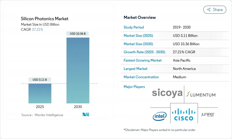
预计到 2025 年,硅光电市场将创造 31.1 亿美元的收入,到 2030 年将达到 103.6 亿美元,年复合成长率为 27.21%。
随着超大规模资料中心从 800G 光链路升级到 1.6T 光链路,汽车 OEM 厂商整合调频连续波雷射雷达,以及政府奖励扩大国内半导体产能,市场需求正在加速成长。北美保持领先地位,但亚太地区正透过大规模晶圆厂扩建缩小差距,以满足 5G、人工智慧和自主供应目标。磷化铟等竞争性材料平台正在推动创新,但也加剧了价格压力。併购活动凸显了光子整合日益增长的战略价值,网路设备供应商、代工厂和云端服务供应商都在努力确保设计团队和晶圆生产能力,以应对迫在眉睫的供应限制。
全球硅光电市场趋势与洞察
在超大规模资料中心采用节能型共封装光元件
将光引擎直接整合到交换器专用积体电路 (ASIC) 旁边,可减少电光转换,并将机架级功耗降低高达 40%。谷歌的光路交换试验已检验延迟有所降低,NVIDIA 和 Marvell 目前都在提供独特的共封装模组样品,这些模组可简化 AI 丛集的电路板布局。随着交换器製造商将光晶片间晶粒标准化,硅光电市场将从中受益,从而推动整合式雷射、调製器和检测器在 300 毫米晶圆上的封装量成长。
碳减量指令促进低功耗光连接模组的发展
欧盟资料中心永续性法规旨在大幅降低能耗,要求业者逐步淘汰铜背板。光子链路可在保持100Gbps通道传输距离的同时,将功耗降低30%。云端服务供应商宣布了碳中和路线蓝图,并加快了400G和800G硅光电模组的多厂商认证,使其符合企业ESG指标和区域绿色交易。
硅基基板的热预算限制超过 70°C
研究计画正在探索具有更高导热性和对温度不敏感的共振器设计的不同材料,但这会增加製程步骤和成本,限制了它们在近期内应用于边缘运算节点。
细分市场分析
随着超大规模资料中心引入 800G 光模组并完成首批 1.6T 线卡的认证,预计 2024 年光收发器市场收入将成长 62%。硅光电市场正朝着将雷射、调製器和检测器整合在单一单晶粒上的全端收发器解决方案转型。市场参与企业正透过模式復用和连续波雷射整合来提高功率效率,从而实现差异化竞争。
晶圆级测试系统正以28.1%的复合年增长率快速成长,主要得益于400G符号/秒以上测试速度对产量比率的严格要求。平行光学探针可缩短测试週期,提高吞吐量,进而满足300毫米生产线的生产能力。供应商正投资于人工智慧辅助缺陷分析,将参数漂移与晶圆厂资料关联起来,以实现预测性维护。自动化光学测试的广泛应用将缩短新产品流片的认证时间,并有助于扩大硅光电市场的规模。
到2024年,主动元件将维持58%的市场份额,这反映出市场对紧凑型连续波雷射、高消光调变器和低暗电流光电二极体的强劲需求。多工器目前已应用于112 Gbaud PAM4收发器中,并在55°C的封装温度下展现出稳定的驱动电压。晶片製造商改进了异质III-V族雷射的附件,提高了电光转换效率并降低了外延界面处的光学损耗。
随着晶圆厂不断改进低损耗波导管、晶格滤波器和针对 400G ZR+ 调谐的阵列波导管光栅,被动元件的复合年增长率 (CAGR) 最高,达到 29.7%。超低粗糙度蚀刻製程可将插入损耗降低至 0.5dB/cm 以下。采用玻璃波导管的印刷光子电路基板可望实现基板级光学背板,进一步拓展硅光电市场的潜在机会。
区域分析
北美地区在《晶片技术创新法案》(CHIPS Act)津贴和人工智慧大型园区快速部署的推动下,预计将在2024年贡献38%的收入。奥尔巴尼奈米科技中心(Albany NanoTech)晋升为国家级研究中心,以及来自云端运算领导企业的私人投资,将打造一个涵盖设计、封装和先进测试的国内生态系统。该地区硅光电市场的持续发展,取决于代工厂和设备供应商之间能否无缝协作,以克服晶圆级散热难题。
亚太地区预计到2030年将以35.1%的复合年增长率实现最快成长,中国、日本和韩国正竞相建立自主供应链。政府补贴涵盖製造工具、培训和计量技术,而5G网路的密集化和本土人工智慧Start-Ups的涌现则确保了市场需求。日本对300毫米GaAs-on-Silicon雷射的投资将推动国内供应商实现出口导向型成长,并增强硅光电市场的全球影响力。
欧洲凭藉欧盟晶片法案提供的数十亿欧元资金筹措以及在汽车、工业自动化和光电研究领域强大的产业基础,继续保持着强劲的发展势头。碳中和资料中心的强制性要求将进一步推动光电的应用。南美以及中东和非洲地区正在为电信和边缘云端部署开闢新的立足点,但仍依赖进口晶粒和封装服务,跨国原始设备製造商(OEM)正寻求透过本地组装伙伴关係关係来填补这一缺口。
其他福利:
- Excel格式的市场预测(ME)表
- 3个月的分析师支持
目录
第一章 引言
- 研究假设和市场定义
- 调查范围
第二章调查方法
第三章执行摘要
第四章 市场情势
- 市场概览
- 市场驱动因素
- 在超大规模资料中心(北美)采用节能型整合光元件
- 促进低功耗光连接模组的碳减排义务(欧盟)
- 5G去程传输/回程传输升级推动 400/800G 模组(亚洲)
- 基于FMCW的汽车级3级光达计画硅光电(中国和欧盟)
- 美国国防部对量子和安全光电的资助
- 政府半导体奖励计画推动光子晶圆厂扩张(美国/欧盟/亚洲)
- 市场限制
- 硅基基板热预算限制超过 70°C
- 缺乏标准化包装会增加非经常性工程成本。
- 在1.55微米以上的波长范围内与InP和聚合物光电竞争
- 300毫米光子晶圆代工厂代工产能有限,导致前置作业时间延长
- 产业生态系分析
- 监理展望
- 技术展望
- 波特五力分析
- 供应商的议价能力
- 买方的议价能力
- 新进入者的威胁
- 替代品的威胁
- 竞争对手之间的竞争
第五章 市场规模与成长预测
- 副产品
- 光收发器
- 光开关
- 主动光缆(AOC)
- 硅光电感测器
- 晶圆级测试系统
- 多工器/解多工器
- 衰减器和调製器
- 其他的
- 按组件
- 主动元件
- 雷射
- 数据机
- 检测器
- 被动元件
- 波导
- 筛选
- 耦合器
- 其他的
- 主动元件
- 按晶圆尺寸
- 300毫米
- 200毫米
- 150毫米或更小
- 按数据速率
- 100 Gbps 或更低
- 200Gbps
- 400Gbps
- 800Gbps
- 1.6 Tbps 或以上
- 透过使用
- 资料中心和高效能运算
- 通讯
- 汽车和自动驾驶汽车
- AR/VR 和消费性电子产品
- 医疗保健和生命科学
- 国防/航太
- 量子计算
- 其他的
- 最终用户
- 超大规模云端供应商
- 通讯业者
- 汽车原始设备製造商和一级供应商
- 医疗设备製造商
- 政府和国防机构
- 研究和学术机构
- 按地区
- 北美洲
- 美国
- 加拿大
- 墨西哥
- 欧洲
- 德国
- 英国
- 法国
- 义大利
- 西班牙
- 其他欧洲地区
- 亚太地区
- 中国
- 日本
- 韩国
- 印度
- 东南亚
- 澳洲
- 亚太其他地区
- 南美洲
- 巴西
- 其他南美洲
- 中东和非洲
- 中东
- 阿拉伯聯合大公国
- 沙乌地阿拉伯
- 其他中东地区
- 非洲
- 南非
- 其他非洲地区
- 北美洲
第六章 竞争情势
- 市场集中度
- 策略趋势
- 市占率分析
- 公司简介
- Intel Corporation
- Cisco Systems Inc.
- Broadcom Inc.
- Lumentum Holdings Inc.
- Juniper Networks Inc.
- GlobalFoundries Inc.
- Sicoya GmbH
- Molex LLC
- Marvell Technology Inc.
- MACOM Technology Solutions
- Coherent Corp.
- Hamamatsu Photonics KK
- Ayar Labs Inc.
- NeoPhotonics Corp.
- IBM Corporation
- Hewlett Packard Enterprise
- II-VI Inc.(now Coherent)
- Rockley Photonics
- Infinera Corporation
- Smart Photonics
- DustPhotonics
- PsiQuantum
- POET Technologies
- Tower Semiconductor
第七章 市场机会与未来展望
The silicon photonics market generates USD 3.11 billion in 2025 and is forecast to advance at a 27.21% CAGR, reaching USD 10.36 billion by 2030.
Demand is accelerating as hyperscale data centers shift from 800 G to 1.6 T optical links, automotive OEMs integrate frequency-modulated continuous-wave LiDAR, and government incentives expand domestic semiconductor capacity. North America retains leadership, yet Asia Pacific is closing the gap through large-scale fab expansions aligned with 5G, AI and sovereign-supply objectives. Competing material platforms such as indium phosphide spur innovation but also intensify price pressure, while thermal-budget ceilings above 70 °C force new cooling architectures. M&A activity underscores the rising strategic value of photonic integration, with network equipment vendors, foundries and cloud providers securing design teams and wafer capacity ahead of looming supply constraints.
Global Silicon Photonics Market Trends and Insights
Energy-efficient Co-Packaged Optics Adoption in Hyperscale Data Centers
Directly embedding optical engines beside switch ASICs trims electrical-optical conversions and cuts rack-level power draw by up to 40%. Google's optical circuit switching trials validate latency gains, and both NVIDIA and Marvell now sample proprietary co-packaged modules that streamline board layouts for AI clusters. The silicon photonics market benefits as switch makers standardize optical die-to-die interfaces, creating a volume pull for integrated lasers, modulators and photodetectors packaged on 300 mm wafers.
Carbon-Reduction Mandates Driving Low-Power Optical Interconnects
EU data-center sustainability rules target significant energy savings, prompting operators to phase out copper backplanes. Photonic links show 30% lower consumption in 100 Gbps channels while maintaining reach. Cloud providers publish carbon-neutral roadmaps, accelerating multi-vendor qualification of 400 G and 800 G silicon photonics modules that align with corporate ESG metrics and local green-deal incentives.
Thermal Budget Limitations in Silicon Substrates Above 70 °C
Optical phase stability drops at elevated junction temperatures, forcing elaborate heat sinks and liquid cooling in tightly packed AI servers.Research programs explore heterogeneous materials with higher thermal conductivity and temperature-insensitive resonator designs, yet these add process steps and cost, tempering near-term adoption in edge compute nodes.
Other drivers and restraints analyzed in the detailed report include:
- 5G Fronthaul/Backhaul Upgrade Fueling 400/800 G Modules
- Automotive Level-3 LiDAR Programs Leveraging FMCW Silicon Photonics
- Lack of Standardized Packaging Elevating NRE Costs
For complete list of drivers and restraints, kindly check the Table Of Contents.
Segment Analysis
Optical transceivers generated 62% revenue in 2024 as hyperscalers deployed 800 G optics and qualified early 1.6 T line-cards.Design wins increasingly bundle integrated drivers and thermal monitors, easing system design and lowering capex per port. The silicon photonics market continues to pivot toward full-stack transceiver solutions that collapse laser, modulator and photodetector in one monolithic die. Market entrants differentiate through modal multiplexing and CW-laser integration that improve power efficiency.
Wafer-level test systems show the fastest expansion at 28.1% CAGR, propelled by tighter yield requirements at 400-G symbols /s and above. Parallel optical probing shrinks cycle time and raises throughput to match 300 mm line capacity. Vendors invest in AI-assisted defect analytics, linking parametric drift to fab data and enabling predictive maintenance. Broader use of automated optical test shortens time-to-qualification for new tape-outs, buttressing scale-up of the silicon photonics market.
Active components maintained a 58% share in 2024, reflecting persistent demand for compact CW lasers, high-extinction modulators and low-dark-current photodiodes. Integrated multiplexers now ship in 112Gbaud PAM4 transceivers, demonstrating stable drive voltages at 55 °C case temperatures. Chip makers refine heterogeneous III-V laser attach, boosting wall-plug efficiency and reducing optical loss across epitaxial interfaces.
Passive components post the highest 29.7% CAGR as fabs iterate low-loss waveguides, lattice filters and arrayed-waveguide gratings tailored for 400G ZR+. Ultralow-roughness etch profiles cut insertion loss below 0.5 dB/cm, essential for co-packaged optics. Printed photonic circuit boards embedding glass waveguides promise board-level optical backplanes, further expanding addressable opportunities for the silicon photonics market.
The Silicon Photonics Market Report is Segmented by Product (Optical Transceivers, Optical Switches, and More), Component (Active, and Passive), Wafer Size (300 Mm, 200 Mm, 150 Mm and Below), Application (Data Centers and High-Performance Computing, Telecommunications, and More), End-User (Hyperscale Cloud Providers, Telecom Operators, and More), and Geography. The Market Forecasts are Provided in Terms of Value (USD).
Geography Analysis
North America generated 38% of 2024 revenue, buoyed by CHIPS Act grants and rapid deployment of AI mega-campuses. Albany NanoTech's elevation to national research hub and private-sector investments from cloud leaders lock in a domestic ecosystem spanning design, packaging and advanced testing. Ongoing evolution of the silicon photonics market in the region hinges on seamless collaboration between foundries and equipment vendors to overcome wafer-level thermal setbacks.
Asia Pacific records the fastest 35.1% CAGR through 2030 as China, Japan and South Korea race to anchor sovereign supply chains. Government subsidies cover fab tools, training and metrology, while 5G densification and local AI start-ups guarantee offtake. Japanese investments in 300 mm GaAs-on-silicon lasers position domestic suppliers for export-oriented growth, reinforcing the global breadth of the silicon photonics market.
Europe sustains momentum through the EU Chips Act's multi-billion-euro financing and a strong industrial base in automotive, industrial automation and research photonics. Carbon-neutral data-center mandates further encourage photonic adoption. South America and the Middle East & Africa open new footholds for telecom and edge-cloud deployments, but still rely on imported dies and packaging services, a gap that multinational OEMs strive to close via localized assembly partnerships.
- Intel Corporation
- Cisco Systems Inc.
- Broadcom Inc.
- Lumentum Holdings Inc.
- Juniper Networks Inc.
- GlobalFoundries Inc.
- Sicoya GmbH
- Molex LLC
- Marvell Technology Inc.
- MACOM Technology Solutions
- Coherent Corp.
- Hamamatsu Photonics K.K.
- Ayar Labs Inc.
- NeoPhotonics Corp.
- IBM Corporation
- Hewlett Packard Enterprise
- II-VI Inc. (now Coherent)
- Rockley Photonics
- Infinera Corporation
- Smart Photonics
- DustPhotonics
- PsiQuantum
- POET Technologies
- Tower Semiconductor
Additional Benefits:
- The market estimate (ME) sheet in Excel format
- 3 months of analyst support
TABLE OF CONTENTS
1 INTRODUCTION
- 1.1 Study Assumptions and Market Definition
- 1.2 Scope of the Study
2 RESEARCH METHODOLOGY
3 EXECUTIVE SUMMARY
4 MARKET LANDSCAPE
- 4.1 Market Overview
- 4.2 Market Drivers
- 4.2.1 Energy-Efficient Co-Packaged Optics Adoption in Hyperscale Data Centers (North America)
- 4.2.2 Carbon-Reduction Mandates Driving Low-Power Optical Interconnects (EU)
- 4.2.3 5G Fronthaul/Backhaul Upgrade Fueling 400/800 G Modules (Asia)
- 4.2.4 Automotive Level-3 LiDAR Programs Leveraging FMCW Silicon Photonics (China and EU)
- 4.2.5 Defense Funding for Quantum and Secure Photonics (United States)
- 4.2.6 Government Semiconductor Incentive Schemes Expanding Photonic Fabs (US/EU/Asia)
- 4.3 Market Restraints
- 4.3.1 Thermal Budget Limitations in Silicon Substrates Above 70 °C
- 4.3.2 Lack of Standardized Packaging Elevating NRE Costs
- 4.3.3 Competition from InP and Polymer Photonics Beyond 1.55 µm
- 4.3.4 Limited 300 mm Photonic Foundry capacity Causing Extended Lead Times
- 4.4 Industry Ecosystem Analysis
- 4.5 Regulatory Outlook
- 4.6 Technological Outlook
- 4.7 Porter's Five Forces Analysis
- 4.7.1 Bargaining Power of Suppliers
- 4.7.2 Bargaining Power of Buyers
- 4.7.3 Threat of New Entrants
- 4.7.4 Threat of Substitutes
- 4.7.5 Intensity of Competitive Rivalry
5 MARKET SIZE AND GROWTH FORECASTS (VALUES)
- 5.1 By Product
- 5.1.1 Optical Transceivers
- 5.1.2 Optical Switches
- 5.1.3 Active Optical Cables (AOCs)
- 5.1.4 Silicon Photonic Sensors
- 5.1.5 Wafer-level Test Systems
- 5.1.6 Multiplexers/De-Multiplexers
- 5.1.7 Attenuators and Modulators
- 5.1.8 Others
- 5.2 By Component
- 5.2.1 Active Components
- 5.2.1.1 Lasers
- 5.2.1.2 Modulators
- 5.2.1.3 Photodetectors
- 5.2.2 Passive Components
- 5.2.2.1 Waveguides
- 5.2.2.2 Filters
- 5.2.2.3 Couplers
- 5.2.2.4 Others
- 5.2.1 Active Components
- 5.3 By Wafer Size
- 5.3.1 300 mm
- 5.3.2 200 mm
- 5.3.3 150 mm and Below
- 5.4 By Data Rate
- 5.4.1 <100 Gbps
- 5.4.2 200 Gbps
- 5.4.3 400 Gbps
- 5.4.4 800 Gbps
- 5.4.5 >1.6 Tbps
- 5.5 By Application
- 5.5.1 Data Centers and High-Performance Computing
- 5.5.2 Telecommunications
- 5.5.3 Automotive and Autonomous Vehicles
- 5.5.4 AR/VR and Consumer Electronics
- 5.5.5 Healthcare and Life Sciences
- 5.5.6 Defense and Aerospace
- 5.5.7 Quantum Computing
- 5.5.8 Others
- 5.6 By End-User
- 5.6.1 Hyperscale Cloud Providers
- 5.6.2 Telecom Operators
- 5.6.3 Automotive OEMs and Tier-1 Suppliers
- 5.6.4 Medical Device Manufacturers
- 5.6.5 Government and Defense Agencies
- 5.6.6 Research and Academic Institutions
- 5.7 By Geography
- 5.7.1 North America
- 5.7.1.1 United States
- 5.7.1.2 Canada
- 5.7.1.3 Mexico
- 5.7.2 Europe
- 5.7.2.1 Germany
- 5.7.2.2 United Kingdom
- 5.7.2.3 France
- 5.7.2.4 Italy
- 5.7.2.5 Spain
- 5.7.2.6 Rest of Europe
- 5.7.3 Asia-Pacific
- 5.7.3.1 China
- 5.7.3.2 Japan
- 5.7.3.3 South Korea
- 5.7.3.4 India
- 5.7.3.5 South East Asia
- 5.7.3.6 Australia
- 5.7.3.7 Rest of Asia-Pacific
- 5.7.4 South America
- 5.7.4.1 Brazil
- 5.7.4.2 Rest of South America
- 5.7.5 Middle East and Africa
- 5.7.5.1 Middle East
- 5.7.5.1.1 United Arab Emirates
- 5.7.5.1.2 Saudi Arabia
- 5.7.5.1.3 Rest of Middle East
- 5.7.5.2 Africa
- 5.7.5.2.1 South Africa
- 5.7.5.2.2 Rest of Africa
- 5.7.1 North America
6 COMPETITIVE LANDSCAPE
- 6.1 Market Concentration
- 6.2 Strategic Moves
- 6.3 Market Share Analysis
- 6.4 Company Profiles (includes Global level Overview, Market level overview, Core Segments, Financials as available, Strategic Information, Market Rank/Share for key companies, Products and Services, and Recent Developments)
- 6.4.1 Intel Corporation
- 6.4.2 Cisco Systems Inc.
- 6.4.3 Broadcom Inc.
- 6.4.4 Lumentum Holdings Inc.
- 6.4.5 Juniper Networks Inc.
- 6.4.6 GlobalFoundries Inc.
- 6.4.7 Sicoya GmbH
- 6.4.8 Molex LLC
- 6.4.9 Marvell Technology Inc.
- 6.4.10 MACOM Technology Solutions
- 6.4.11 Coherent Corp.
- 6.4.12 Hamamatsu Photonics K.K.
- 6.4.13 Ayar Labs Inc.
- 6.4.14 NeoPhotonics Corp.
- 6.4.15 IBM Corporation
- 6.4.16 Hewlett Packard Enterprise
- 6.4.17 II-VI Inc. (now Coherent)
- 6.4.18 Rockley Photonics
- 6.4.19 Infinera Corporation
- 6.4.20 Smart Photonics
- 6.4.21 DustPhotonics
- 6.4.22 PsiQuantum
- 6.4.23 POET Technologies
- 6.4.24 Tower Semiconductor
7 MARKET OPPORTUNITIES AND FUTURE OUTLOOK
- 7.1 White-space and Unmet-Need Assessment
 硅光电市场分析与预测(2034年):类型、产品、服务、技术、组件、应用、材料类型、设备、部署与最终用户
 硅光电市场按产品类型、组件、波导管和最终用途划分-2025-2032年全球预测
 2025年硅光电全球市场报告
 硅光电市场:全球组件、产品、最终用户和地区—2030 年预测
 硅光电市场规模、份额、按组件、产品、最终用户和地区分類的成长分析 - 2025-2032 年产业预测硅光电市场分析及2034年预测:类型、产品、技术、组件、应用、材料类型、设备、流程、最终用户
 硅光子学·光积体电路的全球市场(2025年~2035年)
 硅光子市场:全球产业分析、市场规模、占有率、成长、趋势与未来预测(2025-2032)
 硅光子市场 - 全球产业分析、规模、占有率、成长、趋势及 2032 年预测
 2025-2033 年硅光子市场报告(按产品、组件(光波导、光调製器、光电探测器、波分复用滤波器、雷射)、应用和地区划分)