


 |
市场调查报告书
商品编码
1851086
基板式PCB:市场占有率分析、产业趋势、统计数据和成长预测(2025-2030)Substrate-Like-PCB - Market Share Analysis, Industry Trends & Statistics, Growth Forecasts (2025 - 2030) |
||||||
※ 本网页内容可能与最新版本有所差异。详细情况请与我们联繫。
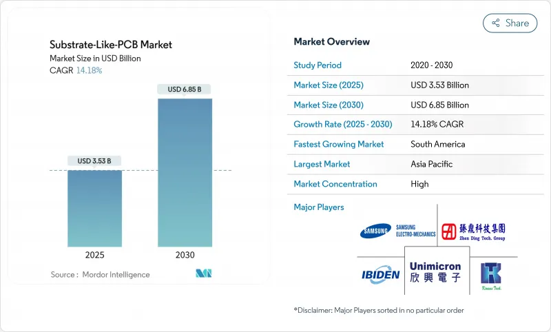
预计到 2025 年,类 PCB基板市场规模将达到 35.3 亿美元,到 2030 年将扩大到 68.5 亿美元,复合年增长率为 14.18%。
随着原始设备製造商 (OEM) 从传统的高密度互连基板过渡到无需完全采用半导体封装即可实现积体电路基板级布线密度的解决方案,市场需求正在加速成长。销售成长主要集中在 5G 无线通讯、人工智慧处理器和汽车高级驾驶辅助系统 (ADAS) 控制器领域,这些领域对讯号完整性要求线宽/间距小于等于 25µm。亚太地区预计将占据 2024 年 69% 的收入,这主要得益于半导体代工厂和 PCB 製造商之间的紧密合作以及对改进型半增材製造生产线的持续投资。由于其低损耗介电特性,ABF 增材膜在材料选择上占据主导地位,但集中化的供应基础正在推动一级製造商之间的垂直整合。 25µm 以下的产量比率优化越来越依赖人工智慧驱动的检测,这为製程控制领域的领导者带来了结构性的成本优势。地缘政治激励奖励,例如美国国防部提供的 3000 万美元津贴,正在提高新参与企业的资格要求,同时也鼓励区域多元化发展。
全球基板PCB市场趋势与洞察
智慧型手机OEM厂商采用高密度互连技术的趋势激增
供应商利用类基板PCB市场技术,将电路密度提高了约30%,从而为5G数据机、AI协处理器和多镜头相机控制等组件腾出更多空间,同时保持设备厚度平坦。旗舰机型的规模经济效益将惠及中阶行动电话,维持高产量生产,从而在更广泛的产品组合中摊提资本成本。
对5G通讯模组的需求不断增长
毫米波基地台板和消费级 5G 无线网卡需要 ≤25µm 的走线宽度,以限制插入损耗和串扰。网路设备製造商 (OEM) 为大规模 MIMO 阵列和波束成形前端指定类基板 PCB 设计,并将基板密度与频谱效率目标挂钩。随着预期数据速率的提高,同样的设计规则也将应用于智慧型手机和平板电脑。
SLP生产线资本支出高
这款待开发区的基板PCB市场产品线需要精密雷射钻孔、直接影像微影术以及1000级无尘室。 1亿美元的支出将迫使规模较小的製造商组成合资企业或退出市场,从而将产能整合到那些拥有雄厚财力的老牌企业手中。
细分市场分析
智慧型手机将在2024年占据类基板PCB市场47%的收入份额,并将在2025年继续保持市场主导地位。此细分市场将充分利用全球行动电话出货量带来的类基板PCB市场规模优势,以实现产能的快速扩张。搭载人工智慧引擎和五天线5G模组的高阶设备需要≤25µm的布线,这将进一步推高尖端市场的需求。随后成本曲线的级联变化将扩大旗舰级产品以外的市场规模,并推动中端市场对此技术的普及。
穿戴式装置是成长最快的细分市场,年复合成长率高达 15.4%,这主要得益于健康监测要求和扩增实境头戴装置的普及。供应商透过将高效电源管理 IC 直接整合到基板中来优化能量密度,从而证明了 SLP 小于 0.5 毫米通孔间距的价值。随着 OEM 厂商指定使用冗余感测器融合板,汽车电子产业的收入来源也更加多元化。网路基础设施和边缘运算闸道正在采用 SLP 来满足散热和延迟目标,而工业和医疗系统则因其严格的可靠性要求而获得更高的平均售价。
到2024年,10-12层PCB将占总产量的37%,在确保布线余量的同时,也兼顾了可控的产量比率风险。这一层数是智慧型手机基板PCB市场规模的支柱。受晶片级AI加速器和汽车域控制器的推动,12层以上的PCB设计正以13%的复合年增长率成长。在此,「基板类PCB市场份额」将属于那些能够掌握连续层压循环中累积翘曲控制的製造商。 8-10层PCB则主要针对对成本敏感的消费物联网产品,并为正在提升SLP(基板类PCB)技术水准的HDI(高密度互连)供应商提供了一条入门途径。
基板型PCB市场依应用领域(智慧型手机、平板电脑、穿戴式装置、汽车电子产品及其他)、堆迭层数(8-10层、10-12层及其他)、基板类型(ABF、改质环氧树脂/FR-4及其他)、线/间距解析度(30/30mm、25/25mm、≤20/20mm)和地区进行细分。市场预测以美元计价。
区域分析
以台湾、韩国和日本为首的亚太地区将在2024年维持69%的营收份额。晶圆代工产业链的生态系统使PCB供应商能够汇集半导体客户的研发成果,进而加速製造设计週期。中国製造商正在积极扩大产能。振鼎科技2024年的营收成长了23%,并有望在2027年之前实现IC基板营收50%的复合年增长率。日本材料巨头正在向该地区供应ABF薄膜,从而增强了区域供应链的密度。
北美地区2024年的贡献将达到18%,这得益于3,000万美元的国防资金和《晶片製造和整合产品法案》(CHIPS Act)的激励措施,用于支付先进工具的成本。 TTM Technologies位于锡拉丘兹的工厂投资1.3亿美元,是北美最大的超高密度整合产品(ultraHDI)投资项目,旨在保障国防供应链的安全。车辆电气化和专用5G网路的部署将对该地区的需求构成结构性抑制。
AT&S在欧洲主导规模虽小但策略性布局,该公司已扩大在马来西亚的生产规模,以满足德国OEM厂商对ADAS电路板的需求。欧盟旨在维护技术主权的津贴将支持SLP生产线的扩张,尤其是在汽车和医疗领域。
南美洲虽然起步较低,但随着近岸外包将轻型组装转移到多明尼加共和国和墨西哥,其复合年增长率达到了12.2%。各国政府正在推动电子产业丛集发展,以创造就业机会并吸引符合自由贸易协定的试点南美洲轻型组装业务投资。
儘管中东和非洲仍在发展中,但主权多元化基金将向半导体后端生态系统注入资金,以保持成长潜力,并随着区域设计工作室的成熟,促进未来基板类PCB市场的渗透。
其他福利:
- Excel格式的市场预测(ME)表
- 3个月的分析师支持
目录
第一章 引言
- 研究假设和市场定义
- 调查范围
第二章调查方法
第三章执行摘要
第四章 市场情势
- 市场概览
- 市场驱动因素
- 智慧型手机OEM厂商采用高密度互连浪涌
- 对5G通讯模组的需求不断增长
- 穿戴式装置和物联网装置小型化趋势
- 用于车载ADAS和电动车电子设备的印刷电路基板日益复杂
- SLP上的覆晶实现异质整合
- 政府对境内先进PCB製造厂的补贴
- 市场限制
- SLP生产线的资本支出较高
- 製程良率在<25mL/S时面临挑战
- 有关特殊积垢化学品的环境法规
- 由于供应商有限,ABF树脂供应有风险。
- 价值/供应链分析
- 监管环境
- 技术展望
- 波特的五力模型
- 供应商的议价能力
- 买方的议价能力
- 新进入者的威胁
- 替代品的威胁
- 竞争的激烈程度
- 产业价值链分析
第五章 市场规模与成长预测
- 透过使用
- 智慧型手机
- 药片
- 穿戴式装置
- 汽车电子产品
- 网路和通讯基础设施
- 物联网/边缘设备
- 工业和医疗用电子设备
- 以堆积层数计算
- 8-10层
- 10-12层
- >12层
- 按基础材料
- ABF(味之素增效膜)
- 改质环氧树脂/FR-4
- 其他(聚四氟乙烯、BT树脂)
- 按线/空分辨率
- 30/30µm
- 25/25µm
- 20/20µm
- 按地区
- 北美洲
- 美国
- 加拿大
- 墨西哥
- 南美洲
- 巴西
- 阿根廷
- 其他南美洲
- 欧洲
- 英国
- 德国
- 法国
- 义大利
- 西班牙
- 俄罗斯
- 其他欧洲地区
- 亚太地区
- 中国
- 日本
- 韩国
- 印度
- 澳洲
- 亚太其他地区
- 中东和非洲
- GCC
- 南非
- 其他中东和非洲地区
- 北美洲
第六章 竞争情势
- 市场集中度
- 策略趋势
- 市占率分析
- 公司简介
- Kinsus Interconnect Technology Corp.
- Ibiden Co., Ltd.
- Compeq Manufacturing Co., Ltd.
- Daeduck Electronics Co., Ltd.
- Unimicron Technology Corp.
- Zhen Ding Technology Holding
- TTM Technologies
- Meiko Electronics Co., Ltd.
- ATandS AG
- Korea Circuit Co., Ltd.
- LG Innotek Co., Ltd.
- Samsung Electro-Mechanics
- Shennan Circuits Co., Ltd.
- Tripod Technology
- Fujitsu Interconnect
- Wus Printed Circuit
- HannStar Board Corp.
- Nippon Mektron Ltd.
- NCAB Group AB
- Multek Ltd.
第七章 市场机会与未来展望
The Substrate-Like PCB market size reached USD 3.53 billion in 2025 and is forecast to advance to USD 6.85 billion by 2030, reflecting a 14.18% CAGR.
Demand accelerates as OEMs migrate from conventional high-density interconnect boards to solutions that deliver IC-substrate-level wiring density without fully moving into semiconductor packaging. Volume growth is anchored in 5G radio, artificial-intelligence processors, and automotive ADAS controllers that require <=25 µm line/space geometries for signal integrity. Asia-Pacific captured 69% of revenue in 2024, benefiting from tight linkages between semiconductor foundries and PCB fabricators plus sustained investment in modified semi-additive processing lines . ABF build-up films dominate material selection on the strength of low-loss dielectric properties, though their concentrated supply base prompts vertical-integration moves by tier-one fabricators. Yield optimization below 25 µm increasingly hinges on AI-enabled inspection, giving process-control leaders a structural cost advantage. Geopolitical reshoring incentives-such as the USD 30 million U.S. Department of Defense grant-add regional diversification while tightening qualification hurdles for new entrants.
Global Substrate-Like-PCB Market Trends and Insights
Surging smartphone OEM adoption for high-density interconnects
Premium handset vendors used Substrate-Like PCB market technology to raise circuit density by roughly 30%, unlocking more space for 5G modems, AI coprocessors, and multi-lens camera control while holding device thickness flat. Scale benefits from flagship models flow into mid-tier phones, sustaining high production runs that amortize capital costs across broader portfolios.
Rising demand for 5G communication modules
Millimeter-wave base-station boards and consumer 5G radio cards require <=25 µm routing to curb insertion loss and crosstalk. Network OEMs specify Substrate-Like PCB market designs for massive-MIMO arrays and beam-forming front ends, linking board density with spectral-efficiency targets. The same design rules migrate into smartphones and tablets as data-rate expectations climb.
High CAPEX for SLP production lines
A greenfield Substrate-Like PCB market line requires precision laser drills, direct-imaging photolithography, and Class 1000 cleanroom space. The USD 100 million outlay pressures smaller fabricators to form joint ventures or exit, consolidating capacity with incumbents that boast balance-sheet depth.
Other drivers and restraints analyzed in the detailed report include:
- Miniaturization trends in wearables & IoT devices
- Automotive ADAS & EV electronics escalating PCB complexity
- Process-yield challenges at <25 µm L/S
For complete list of drivers and restraints, kindly check the Table Of Contents.
Segment Analysis
Smartphones accounted for 47% of Substrate-Like PCB market revenue in 2024 and remain the anchor customer set entering 2025. The segment leverages the Substrate-Like PCB market size advantage inherent in global handset shipments to underwrite rapid capacity ramps. Premium devices that pair AI engines with 5-antenna 5G radios require <=25 µm wiring, reinforcing demand at the leading edge. A cascading cost curve then enables mid-tier adoption, extending volume visibility beyond flagship refreshes.
Wearables are the fastest-growing niche at a 15.4% CAGR, catalyzed by health monitoring mandates and augmented-reality headsets. Suppliers optimize energy density by embedding high-efficiency power-management ICs directly onto the board, proving the value of SLP's sub-0.5 mm via pitch. Automotive electronics add diversified revenue streams as OEMs specify redundant sensor-fusion boards. Networking infrastructure and edge-computing gateways adopt SLP to meet thermal and latency targets, while industrial and medical systems command premium ASPs due to stringent reliability.
The 10-12-layer cohort controlled 37% of 2024 output, balancing routing headroom with manageable yield risk. This stratum remains the workhorse for the Substrate-Like PCB market size tied to smartphone boards. Designs exceeding 12 layers are scaling at 13% CAGR on the back of chiplet-based AI accelerators and automotive domain controllers. Here, "Substrate-Like PCB market share" accrues to fabricators that master cumulative-warp control across sequential lamination cycles. Layer counts of 8-10 serve cost-sensitive consumer IoT products, offering an entry path for HDI vendors up-skilling toward SLP.
Substrate-Like-PCB Market is Segmented by Application (Smartphones, Tablets, Wearables, Automotive Electronics, and More), by Build-Up Layer Count (8 - 10 Layers, 10 - 12 Layers, and More), by Base Material (ABF, Modified Epoxy / FR-4, and More), by Line/Space Resolution (30/30 Mm, 25/25 Mm, and <= 20/20 Mm) and by Geography. The Market Forecasts are Provided in Terms of Value (USD).
Geography Analysis
Asia-Pacific retained a 69% revenue share in 2024, anchored by Taiwan, South Korea, and Japan. Foundry-adjacent ecosystems accelerate design-for-manufacture cycles, letting PCB vendors co-opt R&D from semiconductor customers. Chinese fabricators expand capacity aggressively; Zhen Ding booked 23% top-line growth in 2024 and is steering toward 50% CAGR in IC-substrate revenue through 2027. Material majors in Japan supply ABF films to the region, reinforcing local supply-chain density.
North America contributed 18% in 2024 but benefits from USD 30 million defense funding plus CHIPS Act incentives that defray advanced tooling. TTM Technologies' USD 130 million Syracuse facility constitutes the largest ultra-HDI investment on the continent, targeting secure-supply defense workloads. Automotive electrification and private-network 5G rollouts give regional demand a structural leg.
Europe's smaller yet strategic footprint is led by AT&S, which extended Malaysian production to serve German OEMs needing ADAS boards. EU grants targeting technology sovereignty support incremental SLP lines, especially for automotive and medical verticals.
South America, though starting from a low base, records a 12.2% CAGR as near-shoring shifts light assembly to the Dominican Republic and Mexico. Governments promote electronics clusters for job creation, drawing pilot SLP investment to align with free-trade agreements.
The Middle East and Africa remain nascent but preserve upside through sovereign diversification funds channeling capital into semiconductor back-end ecosystems, enabling future Substrate-Like PCB market penetration once regional design houses mature.
- Kinsus Interconnect Technology Corp.
- Ibiden Co., Ltd.
- Compeq Manufacturing Co., Ltd.
- Daeduck Electronics Co., Ltd.
- Unimicron Technology Corp.
- Zhen Ding Technology Holding
- TTM Technologies
- Meiko Electronics Co., Ltd.
- ATandS AG
- Korea Circuit Co., Ltd.
- LG Innotek Co., Ltd.
- Samsung Electro-Mechanics
- Shennan Circuits Co., Ltd.
- Tripod Technology
- Fujitsu Interconnect
- Wus Printed Circuit
- HannStar Board Corp.
- Nippon Mektron Ltd.
- NCAB Group AB
- Multek Ltd.
Additional Benefits:
- The market estimate (ME) sheet in Excel format
- 3 months of analyst support
TABLE OF CONTENTS
1 INTRODUCTION
- 1.1 Study Assumptions and Market Definition
- 1.2 Scope of the Study
2 RESEARCH METHODOLOGY
3 EXECUTIVE SUMMARY
4 MARKET LANDSCAPE
- 4.1 Market Overview
- 4.2 Market Drivers
- 4.2.1 Surging smartphone OEM adoption for high-density interconnects
- 4.2.2 Rising demand for 5G communication modules
- 4.2.3 Miniaturization trends in wearables and IoT devices
- 4.2.4 Automotive ADAS and EV electronics escalating PCB complexity
- 4.2.5 Flip-chip on SLP enabling heterogeneous integration
- 4.2.6 Government subsidies for on-shore advanced PCB fabs
- 4.3 Market Restraints
- 4.3.1 High CAPEX for SLP production lines
- 4.3.2 Process-yield challenges at <25 m L/S
- 4.3.3 Environmental rules on specialty build-up chemistries
- 4.3.4 Supply risk of ABF resin due to limited vendors
- 4.4 Value / Supply-Chain Analysis
- 4.5 Regulatory Landscape
- 4.6 Technological Outlook
- 4.7 Porters Five Forces
- 4.7.1 Bargaining Power of Suppliers
- 4.7.2 Bargaining Power of Buyers
- 4.7.3 Threat of New Entrants
- 4.7.4 Threat of Substitutes
- 4.7.5 Intensity of Rivalry
- 4.8 Industry Value Chain Analysis
5 MARKET SIZE and GROWTH FORECASTS (VALUE)
- 5.1 By Application
- 5.1.1 Smartphones
- 5.1.2 Tablets
- 5.1.3 Wearables
- 5.1.4 Automotive Electronics
- 5.1.5 Networking and Communication Infrastructure
- 5.1.6 IoT / Edge Devices
- 5.1.7 Industrial and Medical Electronics
- 5.2 By Build-Up Layer Count
- 5.2.1 8 - 10 Layers
- 5.2.2 10 - 12 Layers
- 5.2.3 > 12 Layers
- 5.3 By Base Material
- 5.3.1 ABF (Ajinomoto Build-up Film)
- 5.3.2 Modified Epoxy / FR-4
- 5.3.3 Others (PTFE, BT Resin)
- 5.4 By Line/Space Resolution
- 5.4.1 30 / 30 µm
- 5.4.2 25 / 25 µm
- 5.4.3 20 / 20 µm
- 5.5 By Geography
- 5.5.1 North America
- 5.5.1.1 United States
- 5.5.1.2 Canada
- 5.5.1.3 Mexico
- 5.5.2 South America
- 5.5.2.1 Brazil
- 5.5.2.2 Argentina
- 5.5.2.3 Rest of South America
- 5.5.3 Europe
- 5.5.3.1 United Kingdom
- 5.5.3.2 Germany
- 5.5.3.3 France
- 5.5.3.4 Italy
- 5.5.3.5 Spain
- 5.5.3.6 Russia
- 5.5.3.7 Rest of Europe
- 5.5.4 APAC
- 5.5.4.1 China
- 5.5.4.2 Japan
- 5.5.4.3 South Korea
- 5.5.4.4 India
- 5.5.4.5 Australia
- 5.5.4.6 Rest of APAC
- 5.5.5 Middle East and Africa
- 5.5.5.1 GCC
- 5.5.5.2 South Africa
- 5.5.5.3 Rest of Middle East and Africa
- 5.5.1 North America
6 COMPETITIVE LANDSCAPE
- 6.1 Market Concentration
- 6.2 Strategic Moves
- 6.3 Market Share Analysis
- 6.4 Company Profiles (includes Global level Overview, Market level overview, Core Segments, Financials as available, Strategic Information, Market Rank/Share for key companies, Products and Services, and Recent Developments)
- 6.4.1 Kinsus Interconnect Technology Corp.
- 6.4.2 Ibiden Co., Ltd.
- 6.4.3 Compeq Manufacturing Co., Ltd.
- 6.4.4 Daeduck Electronics Co., Ltd.
- 6.4.5 Unimicron Technology Corp.
- 6.4.6 Zhen Ding Technology Holding
- 6.4.7 TTM Technologies
- 6.4.8 Meiko Electronics Co., Ltd.
- 6.4.9 ATandS AG
- 6.4.10 Korea Circuit Co., Ltd.
- 6.4.11 LG Innotek Co., Ltd.
- 6.4.12 Samsung Electro-Mechanics
- 6.4.13 Shennan Circuits Co., Ltd.
- 6.4.14 Tripod Technology
- 6.4.15 Fujitsu Interconnect
- 6.4.16 Wus Printed Circuit
- 6.4.17 HannStar Board Corp.
- 6.4.18 Nippon Mektron Ltd.
- 6.4.19 NCAB Group AB
- 6.4.20 Multek Ltd.
7 MARKET OPPORTUNITIES and FUTURE OUTLOOK
- 7.1 White-space and Unmet-Need Assessment


