


 |
市场调查报告书
商品编码
1851389
影像感测器:市场份额分析、行业趋势、统计数据和成长预测(2025-2030 年)Image Sensors - Market Share Analysis, Industry Trends & Statistics, Growth Forecasts (2025 - 2030) |
||||||
※ 本网页内容可能与最新版本有所差异。详细情况请与我们联繫。
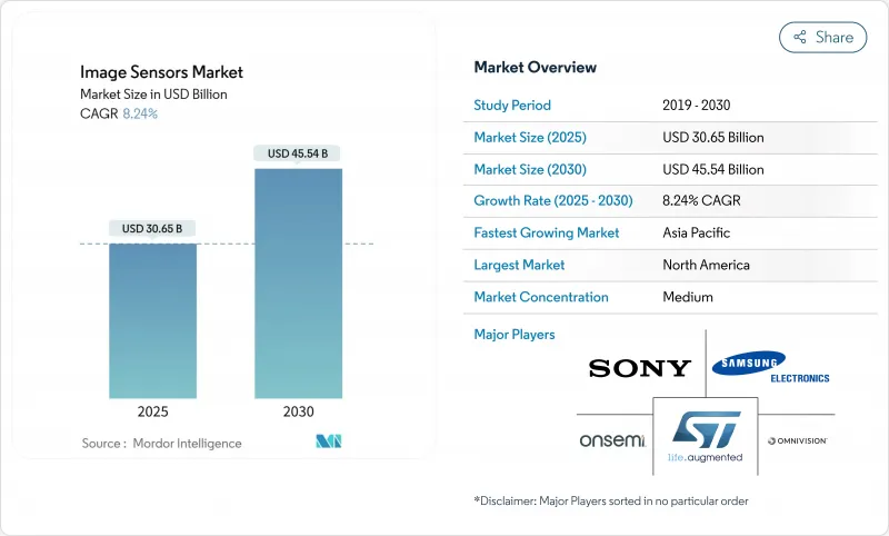
预计到 2025 年,影像感测器市场规模将达到 306.5 亿美元,到 2030 年将扩大到 455.4 亿美元,预测期内复合年增长率将达到 8.24%。
这一增长反映了汽车安全法规、先进的多摄影机智慧型手机以及工业自动化需求的共同作用,这些因素正在再形成半导体需求。汽车製造商计画在2025年每辆车平均增加8个摄影机,到2028年增加12个摄影机,这将加速感测器产量和平均售价的扩张。由于低功耗的片上处理能力,CMOS元件将在2024年占据93%的出货量,而堆迭式背照式(BSI)设计到2030年将以55%的复合年增长率成长,从而在边缘端实现更高的动态范围和人工智慧运算能力。 4-12MP解析度区间占据主导地位,占总收入的32%,在主流消费和工业应用领域兼顾了影像品质和成本。在地缘政治出口限制、300mm晶圆短缺以及热噪声阻碍亚微米像素尺寸缩小等因素的影响下,SONY、三星、OmniVision和安森美半导体正在激烈竞争,以抵御新参与企业的市场份额。
全球影像感测器市场趋势与洞察
汽车影像感测器促进了ADAS和自动驾驶技术的普及。
安森美半导体 (Onsemi) 的 Hyperlux AR0823AT 晶片成功入选Subaru下一代 EyeSight 立体摄影机系统,并达到了自主决策所需的 ASIL-C 安全等级。Canon的 410MP 原型感测器实现了 3280MP/s 的处理速度,证明现代感测器已不再是成像器,而是计算平台。SONY预测,2019 年至 2030 年间,汽车摄影机节点数量将增加 6.68 倍,凸显了 OEM 厂商对高动态范围、低延迟组件的持续需求。 HDR、LED 闪烁抑制和功能安全 IP 现已成为标配,使汽车成像器成为关键的安全基础设施。
亚洲地区配备高解析度CMOS BSI感测器的多相机智慧型手机的渗透率
亚洲行动电话系统持续推动像素架构的突破。三星计划从2025年开始将其华城生产线改造为堆迭式CIS製造,力争赢得高阶iPhone的设计订单。这种三层感测器将光电二极体层、传输和逻辑层分离,在缩小尺寸的同时提升了动态范围。 OmniVision的OV50X采用1.6µm像素实现了110dB的单次曝光HDR,证明了亚洲供应商在低照度计算成像领域的领先地位。从百万像素竞争转向影像品质竞争,凸显了智慧型手机发展週期的日趋成熟,先进的BSI和AI ISP的整合将显着提升用户体验。
300毫米晶圆製造供应链的集中导致价格波动。
儘管SEMI预测2024年晶圆月产能将达到3000万片,但生产集中在少数几家亚洲晶圆代工厂,加剧了需求激增期间的供不应求。目前,影像感测器生产线正与利润更高的AI加速器生产线争夺相同的300毫米光刻设备,导致晶粒价格上涨和前置作业时间延长。据麦肯锡称,微影术所需的特种化学品有60%并非在美国本土供应,增加了上游风险。在亚利桑那州和欧洲的晶圆厂从2026年开始逐步实现量产之前,价格波动可能会持续对整个影像感测器市场的利润率构成压力。
细分市场分析
到2024年,CMOS感测器将占出货量的93%,从而支援低功耗逻辑整合和晶圆成本优势。 CMOS影像感测器市场规模将在2025年达到287亿美元,超过CCD市场。列并行ADC和背面互连技术提高了影格速率,同时缩小了晶粒面积,使得供应商仅在行动电话的年出货量就达到50亿至70亿片。儘管科学研究和医疗设备仍因其超低暗电流而继续订购CCD,但晶圆厂的投资正逐渐转向CMOS,CCD的市占率稳定成长。三星的三层堆迭结构透过分离光电二极体、传输层和逻辑层,提高了量子效率并降低了串扰,巩固了CMOS的领先地位。
第二代堆迭式CIS工艺,凭藉其改进的冗余性和缺陷管理能力,预计到2030年CMOS製程的复合年增长率将达到10.2%。这一成长动能将使来自中国和印度的新兴参与企业能够获得成熟的65nm製程授权,并推出具有竞争力的汽车环景显示图像感测器。随着代工厂为光电模组增加专用的氧化物-绝缘体埋线和混合键合线,CMOS创新仍然是影像感测器市场的主要驱动力。
堆迭式背照式感测器 (BSI) 的出货量正以 55% 的复合年增长率增长,垂直整合突破了二维缩放的限制。光电二极体层和逻辑层的分离使得在不增加晶粒下,能够获得更大的集光面积,从而实现 1.5-2EV 的感光度提升。Canon的 410MP 堆迭式全片幅感测器透过 40 条平行通道实现了 3280MP/s 的读取速度,展现了其高性能潜力。晶圆间混合键结技术正从试生产阶段逐步迈向全天候量产,显着提升了製造产量比率,与硅通孔堆迭技术相比,成本降低了 30%。
在影像感测器市场,受智慧型手机和车载高级驾驶辅助系统(ADAS)日益增长的推动,堆迭式背照式(BSI)预计到2030年将占据259亿美元的市场份额。虽然正面BSI和传统BSI仍将是成本主导型低阶设备的可行选择,但高阶製造商目前正围绕多层堆迭技术调整蓝图,这些技术将ISP模组、SDRAM和AI加速器整合到像素矩阵下方,从而推动系统级封装)的整合。
区域分析
北美仍然是该地区最大的区域买家,ADAS法规和国防采购推动了高规格ASP的需求。美国最终确定了自动紧急煞车规则,该规则实际上强制要求从2029年起所有轻型车辆安装前置摄影机,从而锁定了长期需求。加拿大的一级供应商正涌向安大略省的汽车产业走廊,墨西哥则为美国OEM厂商提供模组组装。该地区半导体自主研发的措施正促使台积电位于亚利桑那州的巨型晶圆厂(投资额达1,650亿美元)从2027年起供应成熟节点的CIS晶圆。
欧洲强调以隐私为先的智慧城市,透过《晶片法案》为边缘人工智慧影像感测器提供资金,欧司朗在奥地利投资 5.88 亿欧元进行扩张,将同时供应汽车雷射雷达和市政交通节点,德国和法国实施了 Euro-NCAP 摄影机基准测试,这将对整个欧洲大陆的供应商产生连锁反应,地方法规限制了脸部云端数据的储存,并鼓励了面部内云和设备内推理感测器。
亚太地区拥有全球最大的晶圆产能和最高的出货量成长率。日本SONY凭藉与一级製造商的合作,目标是在2026年占据汽车CMOS市场43%的份额。韩国三星正在对其华城工厂进行改造,以每月增加20万片晶圆的CIS产能,从而支援智慧型手机和AR/VR相机。中国吉林一号卫星星座的遥感探测需求不断增长,但由于美国对先进的28nm CIS製程节点实施出口限制,国内晶圆代工厂正加速投资成熟製程。印度正在崛起为以消费主导的汽车行车记录器和低成本行动电话市场,而以色列正在其GaAs晶圆厂开发小众国防成像器,进一步扩大了区域多元化。
其他福利:
- Excel格式的市场预测(ME)表
- 3个月的分析师支持
目录
第一章 引言
- 研究假设和市场定义
- 调查范围
第二章调查方法
第三章执行摘要
第四章 市场情势
- 市场概览
- 市场驱动因素
- 汽车级影像感测器加速了ADAS和自动驾驶系统的部署
- 亚洲地区配备高解析度CMOS BSI感测器的多相机智慧型手机的渗透率
- 短波红外线/近红外线感测器在精密农业和工业检测的应用日益广泛
- 边缘人工智慧视觉模组加速了物联网和智慧城市计划的发展,尤其是在欧洲。
- 全球对AR/VR穿戴式装置百叶窗感测器的需求正在上升。
- 北美和日本政府对ADAS摄影机的安全要求
- 市场限制
- 300毫米晶圆厂供应链集中导致价格波动
- 亚微米像素硅的热杂讯和功耗限制,以及进一步提高解析度所面临的挑战
- 对先进成像晶片的出口限制影响中国原始设备製造商
- 短波红外线感测器的高整合成本限制了其在消费性电子产品中的应用。
- 价值/供应链分析
- 监理展望
- 技术展望
- 波特五力分析
- 供应商的议价能力
- 消费者议价能力
- 新进入者的威胁
- 替代品的威胁
- 竞争对手之间的竞争
- 新冠疫情与以色列-加萨衝突的影响评估
第五章 市场规模与成长预测
- 按类型
- CMOS
- CCD
- 透过加工技术
- 前侧照明(FSI)
- 背照式(BSI)
- 堆迭式BSI
- 按百叶窗类型
- 百叶窗
- 全球百叶窗
- 频谱
- 可见光(RGB)
- 近红外线(NIR)
- 短波红外线 (SWIR)
- X射线/紫外线
- 通过决议
- 小于100万像素
- 1-3 MP
- 4-12 MP
- 13-24 MP
- 2500万像素或以上
- 按最终用户行业划分
- 消费性电子产品
- 汽车与运输
- 工业自动化与机器人
- 安全与监控
- 医疗保健和生命科学
- 航太/国防
- 其他(智慧城市、农业、海洋)
- 按地区
- 北美洲
- 美国
- 加拿大
- 墨西哥
- 欧洲
- 英国
- 德国
- 法国
- 义大利
- 其他欧洲地区
- 亚太地区
- 中国
- 日本
- 印度
- 韩国
- 亚太其他地区
- 中东
- 以色列
- 沙乌地阿拉伯
- 阿拉伯聯合大公国
- 土耳其
- 其他中东地区
- 非洲
- 南非
- 埃及
- 其他非洲地区
- 南美洲
- 巴西
- 阿根廷
- 其他南美洲
- 北美洲
第六章 竞争情势
- 市场集中度
- 策略趋势
- 市占率分析
- 公司简介
- Sony Group Corp.
- Samsung Electronics Co., Ltd.
- OmniVision Technologies, Inc.
- STMicroelectronics NV
- ON Semiconductor Corporation
- Canon Inc.
- Panasonic Holdings Corporation
- Teledyne DALSA Inc.
- ams OSRAM AG
- SK hynix Inc.
- GalaxyCore Inc.
- Hamamatsu Photonics KK
- SmartSens Technology
- PixArt Imaging Inc.
- Himax Technologies, Inc.
- Tower Semiconductor Ltd.
- Teledyne e2v
- Gpixel Inc.
- Forza Silicon Corp.
- Toshiba Electronic Devices and Storage Corp.
- Pyxalis SA
第七章 市场机会与未来展望
The image sensor market reached USD 30.65 billion in 2025 and is projected to expand to USD 45.54 billion by 2030, translating to an 8.24% CAGR over the forecast period.
Growth reflects a confluence of automotive safety mandates, sophisticated multi-camera smartphones, and industrial automation needs that are reshaping semiconductor demand. Vehicle makers are equipping an average of 8 cameras per car in 2025 and plan to add 12 cameras by 2028, accelerating sensor volumes and ASP expansion. CMOS devices capture 93% of 2024 unit shipments because of low-power on-chip processing, while stacked back-side-illuminated (BSI) designs, scaling at a 55% CAGR to 2030, unlock higher dynamic range and AI computation at the edge. The 4-12 MP resolution bracket dominates with 32% revenue because it balances image quality and cost for mainstream consumer and industrial use. Competitive intensity is rising as Sony, Samsung, OmniVision and onsemi defend share against new entrants amid geopolitical export controls, 300 mm wafer scarcity, and thermal-noise barriers that slow sub-micron pixel shrink.
Global Image Sensors Market Trends and Insights
Automotive-grade Image Sensors Fueling ADAS & Autonomous Deployment
Automotive safety regulation is shifting cameras from premium options to mandated equipment, transforming the image sensor market. onsemi's Hyperlux AR0823AT won Subaru's next-gen EyeSight stereo-camera slot, meeting ASIL-C targets for autonomous decision making. Canon's prototype 410 MP sensor processes 3,280 MP/s, showing that modern sensors are computational platforms, not passive imagers. Sony projects a 6.68-fold jump in car camera nodes between 2019 and 2030, highlighting sustained OEM pull for high-dynamic-range, low-latency parts. HDR, LED-flicker mitigation and functional-safety IP now come standard, positioning automotive imagers as critical safety infrastructure.
Penetration of Multi-Camera Smartphones with High-Resolution CMOS BSI Sensors in Asia
Asia's handset ecosystem keeps driving pixel-architecture breakthroughs. Samsung converted its Hwaseong line to stacked CIS fabrication starting 2025, chasing premium iPhone design wins. Its 3-layer sensor splits photodiode, transfer and logic strata, boosting dynamic range while shrinking footprint. OmniVision's OV50X delivers 110 dB single-exposure HDR with 1.6 µm pixels, proving Asian suppliers now lead in low-light computational imaging. The shift from megapixel race to image quality underscores a mature smartphone cycle where advanced BSI and AI ISP integration differentiate user experience.
Supply-Chain Concentration in 300 mm Wafer Fabs Creating Price Volatility
SEMI records 30 million wafers-per-month capacity in 2024, yet production clusters around a handful of Asian foundries, amplifying shortages during demand spikes. Image sensor lines now compete with high-margin AI accelerators for the same 300 mm tools, lifting die prices and lengthening lead times. McKinsey observes that 60% of specialty chemicals needed for lithography lack local US supply, adding upstream risk. Until Arizona and European fabs reach volume after 2026, price swings will compress margins across the image sensor market.
Other drivers and restraints analyzed in the detailed report include:
- Growing Adoption of SWIR/NIR Sensors in Precision Agriculture & Industrial Inspection
- Edge-AI-Enabled Vision Modules Accelerating IoT & Smart City Projects
- Thermal Noise & Power Limits in Sub-Micron Pixel Shrink Challenging Further Resolution Gains
For complete list of drivers and restraints, kindly check the Table Of Contents.
Segment Analysis
CMOS sensors owned 93% of unit shipments in 2024, underscoring their low-power logic integration and per-wafer economics. The image sensor market size for CMOS reached USD 28.7 billion in 2025, dwarfing CCD revenues. Column-parallel ADC and backside wiring lift frame rate while shrinking die area, letting vendors ship 5-7 billion parts yearly for phones alone. Scientific and medical instruments continue ordering CCDs for ultra-low dark current, yet fab investments trend to CMOS, ensuring its share rises. Samsung's 3-layer stack demonstrates how separating photodiode, transfer and logic planes lifts quantum efficiency and reduces crosstalk, cementing CMOS leadership.
Second-generation stacked CIS improves redundancy and defect management, driving a projected 10.2% unit CAGR for CMOS through 2030. This momentum allows new entrants from China and India to license mature-node 65 nm flows and still launch competitive imagers for automotive surround-view. The image sensor market remains anchored on CMOS innovation as foundries add buried oxide isolation and hybrid bonding lines dedicated to photonics modules.
Stacked BSI shipments are growing at 55% CAGR because vertical integration circumvents 2-D scaling limits. Separating photodiode and logic layers permits larger light-collection areas without enlarging die, yielding 1.5-2 EV sensitivity uplift. Canon's 410 MP stacked full-frame sensor reads 3,280 MP/s via 40 parallel lanes, showing high-performance potential. Manufacturing yields have risen as wafer-to-wafer hybrid bonding moves from pilot to 24/7 production, cutting cost by 30% versus through-silicon-via stacking.
Within the image sensor market, stacked BSI is forecast to command USD 25.9 billion of image sensor market size by 2030, underpinned by smartphone and automotive ADAS volume ramps. Front-side and conventional BSI remain viable in low-tier devices where cost dominates, but premium makers now align roadmaps around multi-layer stacks that embed ISP blocks, SDRAM and AI accelerators under the pixel matrix, driving system-in-package convergence.
The Image Sensor Market Report is Segmented by Type (CMOS, CCD), Processing Technology (Front-Side Illuminated, Back-Side Illuminated, and More), Shutter Type (Rolling, Global), Spectrum (Visible, Near-Infrared, and More), Resolution (Less Than1 MP, 1-3 MP, and More), End-User Industry (Consumer Electronics, Automotive, Industrial, and More), and Geography. The Market Forecasts are Provided in Terms of Value (USD).
Geography Analysis
North America remains the largest regional buyer measured in revenue because ADAS regulations and defense procurements drive high-spec ASP. The United States finalized automatic emergency braking rules that implicitly require forward-facing cameras in all light vehicles from 2029, locking long-tail demand. Canada's Tier-1 suppliers cluster around Ontario's automotive corridor, and Mexico hosts module assembly for US OEMs. The region's push for semiconductor sovereignty spurred TSMC's USD 165 billion Arizona megafab, anticipated to supply mature-node CIS wafers post-2027.
Europe emphasizes privacy-first smart cities, funding edge-AI image sensors via the Chips Act. ams OSRAM's EUR 588 million Austrian expansion will feed both automotive lidar and municipal traffic nodes. Germany and France enforce Euro-NCAP camera benchmarks that trickle to suppliers across the continent. Local regulations cap cloud storage of facial data, encouraging in-sensor encryption and on-device inference, cultivating a premium for secure image sensor market designs.
Asia-Pacific houses most wafer capacity and posts the fastest shipment growth. Japan's Sony aims for 43% automotive CMOS share by 2026 on the back of Tier-1 alliances. South Korea's Samsung is retooling Hwaseong for additional 200,000 wafers-per-month CIS output to backfill smartphone and AR/VR cameras. China increases remote-sensing demand for its Jilin-1 constellation yet faces US export controls on advanced 28 nm CIS nodes, prompting domestic foundries to accelerate mature-process investments. India emerges as a consumption-driven market for automotive dash-cams and low-cost phones, while Israel develops niche defense imagers in GaAs fabs, extending regional diversity.
- Sony Group Corp.
- Samsung Electronics Co., Ltd.
- OmniVision Technologies, Inc.
- STMicroelectronics N.V.
- ON Semiconductor Corporation
- Canon Inc.
- Panasonic Holdings Corporation
- Teledyne DALSA Inc.
- ams OSRAM AG
- SK hynix Inc.
- GalaxyCore Inc.
- Hamamatsu Photonics K.K.
- SmartSens Technology
- PixArt Imaging Inc.
- Himax Technologies, Inc.
- Tower Semiconductor Ltd.
- Teledyne e2v
- Gpixel Inc.
- Forza Silicon Corp.
- Toshiba Electronic Devices and Storage Corp.
- Pyxalis S.A.
Additional Benefits:
- The market estimate (ME) sheet in Excel format
- 3 months of analyst support
TABLE OF CONTENTS
1 INTRODUCTION
- 1.1 Study Assumptions and Market Definition
- 1.2 Scope of the Study
2 RESEARCH METHODOLOGY
3 EXECUTIVE SUMMARY
4 MARKET LANDSCAPE
- 4.1 Market Overview
- 4.2 Market Drivers
- 4.2.1 Automotive-grade Image Sensors Fueling ADAS and Autonomous Deployment
- 4.2.2 Penetration of Multi-Camera Smartphones with High-Resolution CMOS BSI Sensors in Asia
- 4.2.3 Growing Adoption of SWIR/NIR Sensors in Precision Agriculture and Industrial Inspection
- 4.2.4 Edge-AI-Enabled Vision Modules Accelerating IoT and Smart City Projects, Especially in Europe
- 4.2.5 Rising Demand for Global Shutter Sensors in AR/VR Wearables
- 4.2.6 Government Safety Mandates for ADAS Cameras in North America and Japan
- 4.3 Market Restraints
- 4.3.1 Supply-Chain Concentration in 300 mm Wafer Fabs Creating Price Volatility
- 4.3.2 Thermal Noise and Power Limits in Sub-Micron Pixel Shrink Challenging Further Resolution Gains
- 4.3.3 Export Controls on Advanced Imaging Chips Affecting China-Based OEMs
- 4.3.4 High Integration Cost of SWIR Sensors Limiting Consumer Electronics Adoption
- 4.4 Value / Supply-Chain Analysis
- 4.5 Regulatory Outlook
- 4.6 Technological Outlook
- 4.7 Porter's Five Forces Analysis
- 4.7.1 Bargaining Power of Suppliers
- 4.7.2 Bargaining Power of Consumers
- 4.7.3 Threat of New Entrants
- 4.7.4 Threat of Substitutes
- 4.7.5 Intensity of Competitive Rivalry
- 4.8 Assessment on the Impact of COVID-19 and Israel-Gaza Conflict
5 MARKET SIZE AND GROWTH FORECASTS (VALUE)
- 5.1 By Type
- 5.1.1 CMOS
- 5.1.2 CCD
- 5.2 By Processing Technology
- 5.2.1 Front-Side Illuminated (FSI)
- 5.2.2 Back-Side Illuminated (BSI)
- 5.2.3 Stacked BSI
- 5.3 By Shutter Type
- 5.3.1 Rolling Shutter
- 5.3.2 Global Shutter
- 5.4 By Spectrum
- 5.4.1 Visible (RGB)
- 5.4.2 Near-Infrared (NIR)
- 5.4.3 Short-Wave Infrared (SWIR)
- 5.4.4 X-ray / UV
- 5.5 By Resolution
- 5.5.1 Less than 1 MP
- 5.5.2 1-3 MP
- 5.5.3 4-12 MP
- 5.5.4 13-24 MP
- 5.5.5 Greater than or Equal to 25 MP
- 5.6 By End-User Industry
- 5.6.1 Consumer Electronics
- 5.6.2 Automotive and Transportation
- 5.6.3 Industrial Automation and Robotics
- 5.6.4 Security and Surveillance
- 5.6.5 Healthcare and Life Sciences
- 5.6.6 Aerospace and Defense
- 5.6.7 Others (Smart City, Agriculture, Marine)
- 5.7 By Geography
- 5.7.1 North America
- 5.7.1.1 United States
- 5.7.1.2 Canada
- 5.7.1.3 Mexico
- 5.7.2 Europe
- 5.7.2.1 United Kingdom
- 5.7.2.2 Germany
- 5.7.2.3 France
- 5.7.2.4 Italy
- 5.7.2.5 Rest of Europe
- 5.7.3 Asia-Pacific
- 5.7.3.1 China
- 5.7.3.2 Japan
- 5.7.3.3 India
- 5.7.3.4 South Korea
- 5.7.3.5 Rest of Asia-Pacific
- 5.7.4 Middle East
- 5.7.4.1 Israel
- 5.7.4.2 Saudi Arabia
- 5.7.4.3 United Arab Emirates
- 5.7.4.4 Turkey
- 5.7.4.5 Rest of Middle East
- 5.7.5 Africa
- 5.7.5.1 South Africa
- 5.7.5.2 Egypt
- 5.7.5.3 Rest of Africa
- 5.7.6 South America
- 5.7.6.1 Brazil
- 5.7.6.2 Argentina
- 5.7.6.3 Rest of South America
- 5.7.1 North America
6 COMPETITIVE LANDSCAPE
- 6.1 Market Concentration
- 6.2 Strategic Moves
- 6.3 Market Share Analysis
- 6.4 Company Profiles (includes Global level Overview, Market level overview, Core Segments, Financials as available, Strategic Information, Market Rank/Share, Products and Services, Recent Developments)
- 6.4.1 Sony Group Corp.
- 6.4.2 Samsung Electronics Co., Ltd.
- 6.4.3 OmniVision Technologies, Inc.
- 6.4.4 STMicroelectronics N.V.
- 6.4.5 ON Semiconductor Corporation
- 6.4.6 Canon Inc.
- 6.4.7 Panasonic Holdings Corporation
- 6.4.8 Teledyne DALSA Inc.
- 6.4.9 ams OSRAM AG
- 6.4.10 SK hynix Inc.
- 6.4.11 GalaxyCore Inc.
- 6.4.12 Hamamatsu Photonics K.K.
- 6.4.13 SmartSens Technology
- 6.4.14 PixArt Imaging Inc.
- 6.4.15 Himax Technologies, Inc.
- 6.4.16 Tower Semiconductor Ltd.
- 6.4.17 Teledyne e2v
- 6.4.18 Gpixel Inc.
- 6.4.19 Forza Silicon Corp.
- 6.4.20 Toshiba Electronic Devices and Storage Corp.
- 6.4.21 Pyxalis S.A.
7 MARKET OPPORTUNITIES AND FUTURE OUTLOOK
- 7.1 White-space and Unmet-Need Assessment
 捲帘百叶窗影像感测器市场:按解析度、像素尺寸、技术和应用划分-2026-2032年全球预测
 影像感测器市场分析及预测(至2035年):按类型、产品类型、技术、应用、组件、设备、最终用户、功能及安装类型划分新兴影像感测器技术市场分析及预测(至2035年):按类型、产品类型、技术、组件、应用、材料类型、装置、製程、最终用户和功能划分百叶窗影像感测器市场分析及预测(至2035年):按类型、产品、技术、组件、应用、材料类型、设备、最终用户和功能划分
 全球影像感测器市场:按类型、成像技术、影像类型、解析度、应用、国家和地区划分-产业分析、市场规模、份额及未来预测(2025-2032年)
 2026年全球影像感测器市场报告InGaAs线性影像感测器市场按应用、终端用户产业、像素间距、技术和整合类型划分,全球预测,2026-2032年偏振图像感测器市场:按技术、终端用户产业、像素尺寸、分销管道和应用划分-全球预测,2026-2032年像素阵列检测器市场按产品类型、技术、应用、终端用户产业和销售管道,全球预测,2026-2032年光学影像防手震市场:按组件、技术、应用、分销管道和最终用户划分,全球预测(2026-2032年)