


 |
市场调查报告书
商品编码
1851519
欧洲影像感测器:市场份额分析、行业趋势、统计数据和成长预测(2025-2030 年)Europe Image Sensors - Market Share Analysis, Industry Trends & Statistics, Growth Forecasts (2025 - 2030) |
||||||
※ 本网页内容可能与最新版本有所差异。详细情况请与我们联繫。
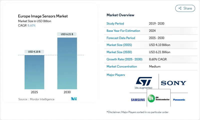
欧洲影像感测器市场预计到 2025 年将达到 41 亿美元,到 2030 年将达到 62.1 亿美元,年复合成长率为 8.66%。
对汽车安全需求的不断增长、智慧型手机摄影机技术的创新以及欧盟半导体共享政策的推行,正共同推动价值创造从家用电子电器领域转向高可靠性的汽车和工业细分市场。晶圆级光学堆迭CMOS成像感测器(CIS)架构与量子点材料在保持轻薄外形的同时,不断提升性能上限。区域性厂商可以利用其与汽车製造商和工业OEM厂商的地理优势,比远距离供应商更快检验功能安全要求。同时,欧洲微影术设备出口限制的不确定性以及不断上涨的能源价格,限制了近期产能扩张,使得厂商优先考虑技术领先优势高于成本的高端细分市场。
欧洲影像感测器市场趋势与洞察
智慧型手机多镜头竞赛 > 200MP
为了与亚洲竞争对手抗衡,欧洲品牌正将感测器解析度提升至2亿像素甚至更高。像素合併技术可在不增加檔案大小的情况下改善低照度性能,而晶圆级光学元件则可降低相机解析度的下降幅度。 OmniVision 的0.56微米像素证明了此技术的可行性,并凸显了温度控管的权衡取舍。如今,设备製造商非常重视欧洲封装专家,他们能够将光学元件、DSP和AI流水线整合到紧凑的外形规格中。随着演算法的成熟和成本曲线的趋于平缓,这项技术的应用将从2026年开始逐步扩展。
欧洲新车安全评估协会(Euro NCAP)强制要求配备前置相机。
欧洲新车安全评鑑协会 (Euro NCAP) 的星级评定係统即将更新,届时所有 2026 年后推出的新车都必须配备前置镜头,用于自动紧急煞车。此规则同样适用于行人及骑乘者侦测,提高了感测器解析度和动态范围的要求。安森美半导体 (OnSemi) 的 Hyperlux 系列产品提供 150dB HDR 分辨率,专为高眩光路况优化,可缩短德国和义大利汽车製造商的检验时间。欧洲一级供应商受益于地理位置优势,靠近测试场地和监管机构,从而缩短了从原型到量产的研发週期。
欧盟高昂的能源和无尘室设施成本
欧洲的电力和超纯水成本比亚洲平均高出30%至50%。碳中和承诺迫使工厂预先支付再生能源合约和暖通空调升级费用。意法半导体(STMicroelectronics)提出的2027年实现碳中和的蓝图凸显了资金方面的限制。规模较小的代工厂由于产量不足以抵消这些成本,要么退出市场,要么转型为精简型晶圆厂模式。欧洲影像感测器市场的参与者正面临短期利润压力,但他们正在赢得注重环境、社会和治理(ESG)的买家的青睐,并建立良好的声誉。
细分市场分析
CMOS感测器凭藉其低功耗和逻辑整合优势,预计将在2024年占据欧洲影像感测器市场86.30%的份额。而对移动车辆和机器人至关重要的全局百叶窗感测器,预计将以9.30%的复合年增长率成长,并在2030年占据欧洲影像感测器市场的大部分份额。捲帘百叶窗CMOS感测器非常适合对价格敏感的行动电话和笔记型电脑,而CCD感测器则主要应用于对超低杂讯要求极高的科学领域。
欧洲企业正利用与汽车製造商的紧密合作关係,共同设计符合ASIL-B认证标准的全局百叶窗零件,从而提前锁定Euro NCAP 2026款车型的设计订单。晶圆级光学元件和深沟槽隔离技术在不增加晶粒尺寸的情况下提高了量子效率。因此,欧洲全局百叶窗装置的影像感测器市场规模预计将强劲成长,即使在消费週期疲软的情况下,也能增强该地区的收入韧性。
2024年,2,500万至6,400万像素的影像感测器将以28.44%的市占率领先市场,在檔案大小和运算工作负载之间取得平衡。然而,2亿像素以上的影像感测器市场将以12.33%的复合年增长率成长,这主要得益于旗舰行动电话无损数位变焦和8K视讯裁剪等功能的推动。随着像素合併演算法的日益成熟,欧洲超高解析度影像感测器市场规模将在2025年至2030年间实现最快成长。
将晶圆级光学元件与亚微米像素对齐的先进封装技术可减少镜头像差,使欧洲模组製造商能够进入高阶手机市场。据观察,欧洲影像感测器市场的原始设备製造商(OEM)正在国内采购特种玻璃和IR滤镜,以应对亚洲供应衝击。入门级手机仍然依赖低于800万像素的晶片,这些晶片受制于捲帘百叶窗的大规模生产。
其他福利:
- Excel格式的市场预测(ME)表
- 包含 3 个月的分析师支持
目录
第一章 引言
- 研究假设和市场定义
- 调查范围
第二章调查方法
第三章执行摘要
第四章 市场情势
- 市场概览
- 市场驱动因素
- 智慧型手机竞相推出2亿像素以上相机
- 欧洲新车安全评鑑协会(Euro NCAP)强制要求前置相机(AEB)
- 晶圆级光学和堆迭式CIS的过渡
- 人工智慧赋能的工业机器视觉补贴
- 抛弃式晶片式医用内视镜
- 欧盟智慧城市监控竞标
- 市场限制
- 欧盟能源成本高企,无尘室公用设施成本高昂
- 300mm CIS级钢材产能有限
- 价值/供应链分析
- 监管环境
- 技术展望
- 波特五力分析
- 供应商的议价能力
- 买方的议价能力
- 新进入者的威胁
- 替代品的威胁
- 竞争对手之间的竞争
第五章 市场规模与成长预测
- 按类型
- CMOS
- CCD
- 通过决议
- 8 MP
- 924 MP
- 2564 MP
- 65200 MP
- 2亿像素以上
- 频谱
- 可见光(RGB)
- 近红外线(NIR)
- 短波红外线 (SWIR)
- 紫外线 (UV)
- 热感/长波红外线
- 透过百叶窗技术
- 捲帘百叶窗CMOS
- 全域百叶窗CMOS
- 按最终用户行业划分
- 消费性电子产品
- 卫生保健
- 工业的
- 安全与监控
- 汽车与运输
- 航太/国防
- 其他终端用户产业
- 按国家/地区
- 英国
- 德国
- 法国
- 义大利
- 其他欧洲地区
第六章 竞争情势
- 市场集中度
- 策略趋势
- 市占率分析
- 公司简介
- STMicroelectronics
- Sony Corporation
- Samsung Electronics Co., Ltd
- On Semiconductor
- OmniVision Technologies
- BAE Systems
- Toshiba Electronic Devices and Storage
- Nikon Corp.
- Panasonic Corp.
- SK Hynix
- Canon Inc.
- AMS-Osram AG
- Teledyne FLIR
- Hamamatsu Photonics
- PixArt Imaging Inc.
- Tower Semiconductor
- Gpixel NV
- Himax Technologies
- GalaxyCore Inc.
- Teledyne e2v
第七章 市场机会与未来展望
The Europe image sensors market stands at USD 4.1 billion in 2025 and is projected to reach USD 6.21 billion by 2030, reflecting an 8.66% CAGR.
Pent-up automotive safety demand, smart-phone camera innovation and EU semiconductor re-shoring policies combine to move value creation from consumer electronics toward high-reliability automotive and industrial niches. Wafer-level optics stacked CMOS imaging sensor (CIS) architectures and quantum-dot materials increase performance ceilings while keeping form factors slim. Regional players leverage proximity to automakers and industrial OEMs to validate functional-safety requirements faster than distant suppliers can. At the same time, export-control uncertainty around lithography tools and high European energy prices temper near-term capacity expansion, pushing firms to prioritize premium segments where technical leadership outweighs cost.
Europe Image Sensors Market Trends and Insights
Multi-camera smartphone race >200 MP
European brands escalate sensor resolution beyond 200 MP to counter Asian rivals. Pixel-binning improves low-light results without ballooning file sizes, while wafer-level optics keeps camera bumps in check. OmniVision's 0.56 µm pixels prove technical feasibility and highlight thermal-management trade-offs. Device makers now value European packaging specialists that co-design optics, DSP and AI pipelines in tight form factors. Adoption is set to widen from 2026 as algorithms mature and cost curves bend.
Euro NCAP AEB front-camera mandate
Euro NCAP's updated star-rating system makes forward-facing cameras compulsory for Automatic Emergency Braking across new models launched from 2026. The rule extends to cyclist and pedestrian detection, increasing sensor resolution and dynamic-range targets. OnSemi's Hyperlux family delivers 150 dB HDR tuned for glare-filled road scenes, lowering validation time for German and Italian OEMs. European tier-1 suppliers benefit from geographical proximity to test tracks and regulatory bodies, shortening loop times between prototype and series production.
High EU energy and clean-room utility costs
Electricity and ultra-pure water bills in Europe sit 30-50% above Asian averages. Carbon-neutrality pledges force fabs to pre-pay for renewable power contracts and HVAC upgrades. STMicroelectronics' roadmap to reach carbon neutrality by 2027 exemplifies the capital drag. Smaller foundries lacking volume to offset these overheads either exit or pivot to fab-lite models. Europe image sensors market players see near-term margin squeeze yet gain reputational leverage with ESG-focused buyers.
Other drivers and restraints analyzed in the detailed report include:
- Wafer-level optics and stacked CIS migration
- AI-enabled industrial machine-vision grants
- Limited 300 mm CIS-grade capacity
For complete list of drivers and restraints, kindly check the Table Of Contents.
Segment Analysis
CMOS sensors captured 86.30% of Europe image sensors market share in 2024 on the back of lower power draw and logic integration. Global-shutter variants, vital for motion-heavy automotive and robotics tasks, are pacing at 9.30% CAGR and will command a larger slice of the Europe image sensors market by 2030. Rolling-shutter CMOS stays relevant for price-sensitive phones and laptops, while CCD retreats into scientific niches where ultra-low noise still matters.
European firms exploit close ties with automakers to co-design ASIL-B qualified global-shutter parts, gaining early design-wins for Euro NCAP 2026 models. Wafer-level optics and deep-trench isolation raise quantum efficiency without inflating die size. Consequently, Europe image sensors market size for global-shutter devices is projected to climb steadily, lifting regional revenue resilience even if consumer cycles soften.
The 25-64 MP class led revenue with 28.44% share in 2024, balancing file-size economy and computational workload. However, >200 MP parts rise at 12.33% CAGR, fuelled by flagship phones that tout lossless digital zoom and 8K video crops. Europe image sensors market size for these ultra-resolution devices will expand fastest in 2025-2030 as pixel-binning algorithms mature.
Packaging advances that align wafer-level optics with sub-µm pixels curb lens aberration, letting European module makers enter premium handset SKUs. The Europe image sensors market observes OEMs procuring specialty glass and IR filters domestically to hedge against Asian supply shocks. Entry-level handsets still rely on <=8 MP chips, keeping a floor under high-volume rolling-shutter production.
The Europe Image Sensors Market is Segmented by Type (CMOS, CCD), Resolution (<= 8 MP, 9 - 24 MP and More), Spectrum (Visible (RGB), Near-Infrared (NIR) and More), Shutter Technology, End-User Industry (Consumer Electronics, Healthcare, and More), and Country. The Market Forecasts are Provided in Terms of Value (USD).
List of Companies Covered in this Report:
- STMicroelectronics
- Sony Corporation
- Samsung Electronics Co., Ltd
- On Semiconductor
- OmniVision Technologies
- BAE Systems
- Toshiba Electronic Devices and Storage
- Nikon Corp.
- Panasonic Corp.
- SK Hynix
- Canon Inc.
- AMS-Osram AG
- Teledyne FLIR
- Hamamatsu Photonics
- PixArt Imaging Inc.
- Tower Semiconductor
- Gpixel NV
- Himax Technologies
- GalaxyCore Inc.
- Teledyne e2v
Additional Benefits:
- The market estimate (ME) sheet in Excel format
- 3 months of analyst support
TABLE OF CONTENTS
1 INTRODUCTION
- 1.1 Study Assumptions and Market Definition
- 1.2 Scope of the Study
2 RESEARCH METHODOLOGY
3 EXECUTIVE SUMMARY
4 MARKET LANDSCAPE
- 4.1 Market Overview
- 4.2 Market Drivers
- 4.2.1 Multi-camera smartphone race beyond 200 MP
- 4.2.2 Euro NCAP front-camera mandate (AEB)
- 4.2.3 Wafer-level optics and stacked CIS migration
- 4.2.4 AI-enabled industrial machine-vision grants
- 4.2.5 Disposable chip-on-tip medical endoscopy
- 4.2.6 EU smart-city surveillance tenders
- 4.3 Market Restraints
- 4.3.1 High EU energy and clean-room utility costs
- 4.3.2 Limited 300 mm CIS-grade capacity
- 4.4 Value / Supply-Chain Analysis
- 4.5 Regulatory Landscape
- 4.6 Technological Outlook
- 4.7 Porters Five Forces Analysis
- 4.7.1 Bargaining Power of Suppliers
- 4.7.2 Bargaining Power of Buyers
- 4.7.3 Threat of New Entrants
- 4.7.4 Threat of Substitutes
- 4.7.5 Intensity of Competitive Rivalry
5 MARKET SIZE AND GROWTH FORECASTS (VALUE)
- 5.1 By Type
- 5.1.1 CMOS
- 5.1.2 CCD
- 5.2 By Resolution
- 5.2.1 8 MP
- 5.2.2 924 MP
- 5.2.3 2564 MP
- 5.2.4 65200 MP
- 5.2.5 > 200 MP
- 5.3 By Spectrum
- 5.3.1 Visible (RGB)
- 5.3.2 Near-Infrared (NIR)
- 5.3.3 Short-Wave IR (SWIR)
- 5.3.4 Ultraviolet (UV)
- 5.3.5 Thermal / LWIR
- 5.4 By Shutter Technology
- 5.4.1 Rolling-Shutter CMOS
- 5.4.2 Global-Shutter CMOS
- 5.5 By End-User Industry
- 5.5.1 Consumer Electronics
- 5.5.2 Healthcare
- 5.5.3 Industrial
- 5.5.4 Security and Surveillance
- 5.5.5 Automotive and Transportation
- 5.5.6 Aerospace and Defense
- 5.5.7 Other End-user Industries
- 5.6 By Country
- 5.6.1 United Kingdom
- 5.6.2 Germany
- 5.6.3 France
- 5.6.4 Italy
- 5.6.5 Rest of Europe
6 COMPETITIVE LANDSCAPE
- 6.1 Market Concentration
- 6.2 Strategic Moves
- 6.3 Market Share Analysis
- 6.4 Company Profiles (includes Global-level Overview, Market-level Overview, Core Segments, Financials as available, Strategic Information, Market Rank/Share for key companies, Products and Services, and Recent Developments)
- 6.4.1 STMicroelectronics
- 6.4.2 Sony Corporation
- 6.4.3 Samsung Electronics Co., Ltd
- 6.4.4 On Semiconductor
- 6.4.5 OmniVision Technologies
- 6.4.6 BAE Systems
- 6.4.7 Toshiba Electronic Devices and Storage
- 6.4.8 Nikon Corp.
- 6.4.9 Panasonic Corp.
- 6.4.10 SK Hynix
- 6.4.11 Canon Inc.
- 6.4.12 AMS-Osram AG
- 6.4.13 Teledyne FLIR
- 6.4.14 Hamamatsu Photonics
- 6.4.15 PixArt Imaging Inc.
- 6.4.16 Tower Semiconductor
- 6.4.17 Gpixel NV
- 6.4.18 Himax Technologies
- 6.4.19 GalaxyCore Inc.
- 6.4.20 Teledyne e2v
7 MARKET OPPORTUNITIES AND FUTURE OUTLOOK
- 7.1 White-space and Unmet-need Assessment
 影像感测器市场:2026-2032年全球市场预测(按感测器类型、波长范围、解析度、处理方法、终端用户产业和分销管道划分)
 2026年全球车载监视摄影机市场报告2026年全球HDR影像讯号处理设备市场报告
 光学影像防手震(OIS)市场规模、份额和成长分析:按技术架构、执行器类型、应用、轴向方向和地区划分-2026-2033年产业预测捲帘百叶窗影像感测器市场:按解析度、像素尺寸、技术和应用划分-2026-2032年全球预测
 影像感测器市场分析及预测(至2035年):按类型、产品类型、技术、应用、组件、设备、最终用户、功能及安装类型划分新兴影像感测器技术市场分析及预测(至2035年):按类型、产品类型、技术、组件、应用、材料类型、装置、製程、最终用户和功能划分百叶窗影像感测器市场分析及预测(至2035年):按类型、产品、技术、组件、应用、材料类型、设备、最终用户和功能划分
 全球影像感测器市场:按类型、成像技术、影像类型、解析度、应用、国家和地区划分-产业分析、市场规模、份额及未来预测(2025-2032年)2026年全球影像感测器市场报告