


 |
市场调查报告书
商品编码
1910440
电子设计自动化工具(EDA):市场占有率分析、产业趋势与统计、成长预测(2026-2031)Electronic Design Automation Tools (EDA) - Market Share Analysis, Industry Trends & Statistics, Growth Forecasts (2026 - 2031) |
||||||
※ 本网页内容可能与最新版本有所差异。详细情况请与我们联繫。
预计到 2026 年,电子设计自动化 (EDA) 工具市场规模将达到 207.8 亿美元,高于 2025 年的 192.2 亿美元。
预计到 2031 年将达到 306.7 亿美元,2026 年至 2031 年的复合年增长率为 8.1%。
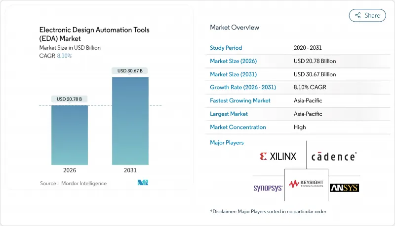
这一前景基于晶体管尺寸的加速缩小、人工智慧驱动的设计流程以及晶圆代工厂与设计工具之间日益密切的合作。晶片设计人员正从手动规则调整转向数据驱动的最佳化,从而缩短流片週期并降低返工风险。云端容量的激增正在扩大先进检验技术的使用范围,而汽车功能安全法规则推动形式化方法进入主流设计领域。 Synopsys 以 350 亿美元收购 Ansys 的交易预计将于 2025 年完成,这标誌着设计领域正系统性地转向整合装置系统平台,该平台能够同时优化晶片、封装和系统的效能。同时,地缘政治出口限制正在催生并行的 EDA 生态系统,迫使供应商为多个地区的晶圆代工厂认证流程,以避免收入损失。
全球电子设计自动化工具 (EDA) 市场趋势与洞察
先进节点晶片密度快速提升
与7nm製程相比,全环栅(GAA)电晶体、背面供电技术和多晶片封装使设计规则检查(DRC)的数量增加了10倍。目前,晶圆代工厂正与EDA领导企业合作开发相关流程,Synopsys和台积电已于2025年4月完成了A16和N2P节点完整数位和类比工具链的认证。统一的探索到最终确认流程可减少代价高昂的重新设计,在3nm製程下,每次重新设计的成本可能超过5000万美元。英特尔的18A计画也同样依赖整合流程,用于将运算、记忆体和I/O整合在单一基板上的2.5D/3D架构。
人工智慧/机器学习加速器和客製化SoC的兴起
超大规模和边缘运算提供者正在加速采用专用推理晶片。 Cadence 报告称,其 2025 年第一季半导体 IP 营收年增 40%,并将这一成长归功于人工智慧和晶片组计划。 NVIDIA、ASML、台积电和 Synopsys 的 CuLitho 软体堆迭将微影术模拟速度提高了 40 倍,从而能够实现满足人工智慧能效目标的光罩版图布局。随着加速器异质性的增加,SIP 的重用和封装内互连标准的标准化正在推动对 IP检验的需求。
主要EDA套件的授权成本不断上涨
用于全面3nm製程签核的企业级年度套餐价格现已超过每席100万美元,迫使中型晶圆厂优先考虑工具模组并延长更新周期。寡占的供应结构维持了供应商的定价权,尤其是在时序收敛和微影术软体包领域,因为目前尚无开放原始码替代方案。
细分市场分析
半导体智慧财产权(SIP)预计将以9.7%的复合年增长率在所有工具类别中位居榜首,这主要得益于晶片组架构的兴起,此类架构需要检验的介面模组和混合讯号核心。到2025年,SIP将占电子设计自动化(EDA)市场收入的18.74%,随着晶圆代工厂推行「已知良品晶粒」策略,每个计划的SIP附加率将比2023年翻倍。受单片SoC向异构封装过渡的推动,SIP应用的EDA市场规模预计将在2031年之前显着成长。
由于布局布线、静态时序和 DRC 在整个流片过程中至关重要,IC 物理设计和检验部分保持了 35.82% 的份额,但透过 AI 增强的布局规划实现的多目标优化自动化,已将最近的 3nm 设计的周转时间缩短了 30%。
前端设计工具的复合年增长率 (CAGR) 为 9.35%,这主要得益于高级综合 (HLS) 和自然语言到 RTL 生成工具等生产力提昇技术的进步。预计到 2031 年,RTL 自动化领域的电子设计自动化 (EDA) 市场规模将显着成长,这主要得益于人工智慧辅助程式码产生技术能够以更少的迭代次数捕捉功能意图。布局、布线和时序收敛仍然占据电子设计自动化 (EDA) 市场份额的 32.10%,这反映了签核级时序收敛和高级 3D 寄生参数提取技术的不可替代性。
目前,生成式设计平台产生的布局指导与手动编写的脚本相比,可将导线长度减少 11%,漏电流减少 9%。然而,最终的系统单晶片 (SoC) 交付仍然需要代工厂核准的认证时序和电气规则报告,这凸显了成熟的后端工具链的重要性。
电子设计自动化工具 (EDA) 报告按工具类型(例如,电脑辅助设计、积体电路实体设计与检验)、设计流程阶段(例如,前端设计 RTL)、部署模式(例如,本地部署、云端部署)、最终用户产业(例如,通讯基础设施、家用电子电器)和地区(例如,北美)进行细分。市场预测以美元计价。
区域分析
亚太地区将在2025年占据42.05%的市场份额,并在2031年之前以9.55%的复合年增长率增长。台湾和韩国的晶圆代工厂群聚将支撑区域工具需求,而中国正加速建造其自主研发的EDA堆迭,以应对美国的出口限制。政府主导的措施正在为人工智慧辅助的布局布线引擎和SPICE模拟器提供补贴,旨在3nm製程量产前实现流程在地化。凭藉印度丰富的工程人才资源,当地设计服务公司在2024年成长了17%,以满足西方客户对高性价比RTL和DFT支援的需求。
北美凭藉主导,保持着其影响力。儘管该地区的市占率将在2025年略微下降至29.15%,但它仍然是先进节点参考工具流程的主要来源。出口管制制度要求供应商对许可证金钥实施地理围栏,这增加了合规成本,并锁定了北美的智慧财产权链。英特尔晶圆代工和新思科技在18A认证流程的合作,加强了美国重夺先进製造业市场份额的努力。欧洲正专注于汽车和工业应用,ISO 26262标准正在推动高端检验工具的普及。台积电计画于2025年在慕尼黑开设设计中心,旨在将晶圆代工厂工程师融入区域供应链,并为3DIC封装和低功耗人工智慧加速器提供直接支援。欧盟晶片津贴将优先为电子设计丛集提供研发税额扣抵,进一步刺激区域电子设计自动化(EDA)技术的应用。中东、非洲和南美洲仍然是发展中地区,但在政府主导的晶圆製造计划和物联网部署取得进展的地区,这些地区正呈现两位数的成长。
其他福利:
- Excel格式的市场预测(ME)表
- 3个月的分析师支持
目录
第一章 引言
- 研究假设和市场定义
- 调查范围
第二章调查方法
第三章执行摘要
第四章 市场情势
- 市场概览
- 市场驱动因素
- 先进节点晶片密度快速提升
- 人工智慧/机器学习加速器和客製化SoC的普及
- 云端原生EDA工作流程(EDA即服务)的兴起
- 汽车产业 ISO 26262 功能安全标准合规性要求
- 开放原始码硬体的普及正在推动检验的需求。
- 美国出口管制政策的两极化加速了国内设计流程的发展。
- 市场限制
- 主要EDA套件的授权成本不断上涨
- 5奈米及以下製程的物理设计工程师短缺
- 云端采用过程中知识产权侵权和网路入侵的风险
- 摩尔定律的延伸速度比预期慢
- 价值链分析
- 监管环境
- 技术展望
- 波特五力分析
- 供应商的议价能力
- 买方的议价能力
- 新进入者的威胁
- 替代品的威胁
- 竞争对手之间的竞争
- 投资分析
- 宏观经济因素如何影响市场
第五章 市场规模与成长预测
- 按工具类型
- 电脑辅助工程(CAE)
- 积体电路物理设计与检验
- 印刷基板(PCB)和多晶片模组(MCM)
- 半导体智慧财产权(SIP)
- 服务
- 按阶段设计流程
- 前端设计(RTL)
- 逻辑综合和功能检验
- 布局、布线和时序收敛
- 最终核准(DFM、电源、SI、散热设计)
- 透过部署模式
- 本地部署
- 基于云端的
- 按最终用户行业划分
- 通讯基础设施
- 家用电子电器
- 汽车与出行
- 工业和能源
- 航太/国防
- 医疗设备
- 其他行业
- 按地区
- 北美洲
- 美国
- 加拿大
- 墨西哥
- 南美洲
- 巴西
- 阿根廷
- 南美洲其他地区
- 欧洲
- 德国
- 英国
- 法国
- 义大利
- 其他欧洲地区
- 亚太地区
- 中国
- 日本
- 韩国
- 印度
- 亚太其他地区
- 中东
- 沙乌地阿拉伯
- 阿拉伯聯合大公国
- 其他中东地区
- 非洲
- 南非
- 其他非洲地区
- 北美洲
第六章 竞争情势
- 市场集中度
- 策略趋势
- 市占率分析
- 公司简介
- Ansys Inc.
- Cadence Design Systems Inc.
- Synopsys Inc.
- Siemens Digital Industries Software(Mentor Graphics)
- Keysight Technologies Inc.
- Altium Limited
- Zuken Ltd.
- Xilinx Inc.(AMD Adaptive and Embedded Computing Group)
- Aldec Inc.
- Agnisys Inc.
- Lauterbach GmbH
- Silvaco Inc.
- Real Intent Inc.
- Axiomise Ltd.
- Imperas Software Ltd.
- PDF Solutions Inc.
- Flex Logix Technologies Inc.
- Andes Technology Corp.
- Cobham Gaisler AB
- Arteris Inc.
第七章 市场机会与未来展望
Electronic Design Automation Tools market size in 2026 is estimated at USD 20.78 billion, growing from 2025 value of USD 19.22 billion with 2031 projections showing USD 30.67 billion, growing at 8.1% CAGR over 2026-2031.
The outlook builds on faster transistor scaling, AI-enabled design flows, and closer foundry-tool collaboration. Chip architects are shifting from manual rule tuning to data-driven optimization that shortens tape-out cycles and lowers re-spin risk. Cloud-based capacity bursting is widening access to advanced verification, while automotive functional-safety mandates push formal methods into mainstream design. The 2025 completion of Synopsys' USD 35 billion acquisition of Ansys signals a systemic move toward unified device-to-system platforms able to co-optimize silicon, package, and full-system performance simultaneously. Meanwhile, geopolitical export controls spur parallel EDA ecosystems, compelling vendors to certify flows for multiple regional foundries to avoid revenue erosion.
Global Electronic Design Automation Tools (EDA) Market Trends and Insights
Soaring Chip-Density in Advanced Nodes
Gate-All-Around transistors, backside power delivery, and multi-die packaging produce a ten-fold rise in design-rule checks compared with 7 nm processes. Foundries now co-develop flows with EDA leaders; Synopsys and TSMC certified full digital and analog toolchains for A16 and N2P nodes in April 2025. Unified exploration-to-signoff environments reduce costly re-spins-each exceeding USD 50 million at 3 nm. Intel's 18A program likewise relies on integrated flows for 2.5D/3D architectures that merge compute, memory, and I/O on a single substrate.
Proliferation of AI/ML Accelerators and Custom SoCs
Hyperscale and edge providers increasingly commission purpose-built inference silicon. Cadence posted 40% YoY growth in semiconductor IP revenue in Q1 2025, attributing momentum to AI and chiplet projects. NVIDIA, ASML, TSMC, and Synopsys reported 40X lithography simulation speed-ups through the CuLitho software stack, enabling reticle layouts that meet AI power-per-watt targets. As accelerator heterogeneity rises, SIP reuse and on-package interconnect standards intensify demand for IP verification.
Escalating Licensing Costs for Leading EDA Suites
Annual enterprise bundles for comprehensive 3 nm sign-off now exceed USD 1 million per seat, forcing mid-tier fabs to prioritize tool modules and extend refresh cycles. Oligopolistic supply means price leverage remains with vendors, particularly for timing closure and lithography simulation packages that have no open-source substitute.
Other drivers and restraints analyzed in the detailed report include:
- Rise of Cloud-Native EDA Workflows (EDA-as-a-Service)
- Automotive ISO 26262 Functional-Safety Compliance Needs
- Talent Shortage in Sub-5 nm Physical-Design Engineers
For complete list of drivers and restraints, kindly check the Table Of Contents.
Segment Analysis
Semiconductor Intellectual Property (SIP) posted a 9.7% CAGR forecast, the fastest among tool categories, owing to rising chiplet architectures that favor verified interface blocks and mixed-signal cores. In 2025, SIP accounted for 18.74% of the Electronic Design Automation Tools market revenue, yet its attach rate per project has doubled since 2023 as foundries promote known-good-die strategies. The Electronic Design Automation Tools market size for SIP applications is projected to grow at a significant rate by 2031, underscoring the shift from monolithic SoCs to heterogeneous assembly.
IC Physical Design and Verification retained a 35.82% share thanks to the mandatory nature of placement, routing, static-timing, and DRC in every tape-out. However, AI-enhanced floorplanning automates multi-objective optimization, shrinking turnaround time by 30% on recent 3 nm designs.
Front-End Design tools record a 9.35% CAGR as high-level synthesis (HLS) and natural-language-to-RTL generators improve productivity. The Electronic Design Automation Tools market size for RTL automation is projected to grow significantly by 2031 on the back of AI-assisted code generation that captures functional intent in fewer iterations. Layout, Routing, and Timing Closure still governs 32.10% of the Electronic Design Automation Tools market share, reflecting the irreplaceable nature of sign-off-caliber timing convergence and advanced 3D parasitic extraction.
Generative design platforms now produce placement guidance that reduces wire length by 11% and leakage by 9% versus human scripts. Yet final SOC hand-off still relies on certified timing and electrical-rule reports accepted by foundries, cementing the relevance of established back-end toolchains.
The Electronic Design Automation Tools Report is Segmented by Tool Type (Computer-Aided Engineering, IC Physical Design and Verification, and More), Design-Flow Stage (Front-End Design RTL, and More), Deployment Mode (On-Premise, and Cloud-Based), End-User Industry (Communication Infrastructure, Consumer Electronics, and More), and Geography (North America, and More). The Market Forecasts are Provided in Terms of Value (USD).
Geography Analysis
Asia-Pacific held a 42.05% share in 2025 and advances at a 9.55% CAGR to 2031. Foundry clustering in Taiwan and South Korea anchors regional tool demand, while China accelerates sovereign EDA stacks in response to U.S. export controls. State-backed initiatives channel subsidies toward AI-assisted place-and-route engines and SPICE simulators, aiming to localize flows before 3 nm production ramps. India leverages a large engineering base; design-service firms there grew 17% in 2024 as Western customers sought cost-effective RTL and DFT support.
North America retains influence through leadership in AI algorithms, IP catalogs, and cloud infrastructure. The region's share contracted slightly to 29.15% in 2025, yet remains the primary source of reference tool flows for leading-edge nodes. Export-control regimes require vendors to implement license-key geofencing, adding compliance cost but also locking in North American IP chains. Collaboration between Intel Foundry and Synopsys on 18A certified flows reinforces the U.S. bid to regain advanced manufacturing share. Europe focuses on automotive and industrial applications, with ISO 26262 driving premium verification tool adoption. TSMC's 2025 design center launch in Munich aims to embed foundry engineers within the regional supply chain, providing first-hand support for 3D-IC packaging and power-efficient AI accelerators. The EU Chips Act grants emphasize RandD tax credits for electronic-design clusters, further stimulating regional EDA uptake. Middle East and Africa and South America remain nascent, but showing double-digit growth where government fab projects or IoT rollouts emerge.
- Ansys Inc.
- Cadence Design Systems Inc.
- Synopsys Inc.
- Siemens Digital Industries Software (Mentor Graphics)
- Keysight Technologies Inc.
- Altium Limited
- Zuken Ltd.
- Xilinx Inc. (AMD Adaptive and Embedded Computing Group)
- Aldec Inc.
- Agnisys Inc.
- Lauterbach GmbH
- Silvaco Inc.
- Real Intent Inc.
- Axiomise Ltd.
- Imperas Software Ltd.
- PDF Solutions Inc.
- Flex Logix Technologies Inc.
- Andes Technology Corp.
- Cobham Gaisler AB
- Arteris Inc.
Additional Benefits:
- The market estimate (ME) sheet in Excel format
- 3 months of analyst support
TABLE OF CONTENTS
1 Introduction
- 1.1 Study Assumptions and Market Definition
- 1.2 Scope of the Study
2 Research Methodology
3 Executive Summary
4 Market Landscape
- 4.1 Market Overview
- 4.2 Market Drivers
- 4.2.1 Soaring chip?density in advanced nodes
- 4.2.2 Proliferation of AI/ML accelerators and custom SoCs
- 4.2.3 Rise of cloud?native EDA workflows (EDA-as-a-Service)
- 4.2.4 Automotive ISO 26262 functional-safety compliance needs
- 4.2.5 Growing open-source hardware movement driving verification demand
- 4.2.6 U.S.-China export-control bifurcation accelerating on-shore design flows
- 4.3 Market Restraints
- 4.3.1 Escalating licensing costs for leading EDA suites
- 4.3.2 Talent shortage in sub-5 nm physical-design engineers
- 4.3.3 IP-theft and cyber-intrusion risks in cloud deployments
- 4.3.4 Slower than expected Moore's-Law cadence extensions
- 4.4 Value Chain Analysis
- 4.5 Regulatory Landscape
- 4.6 Technological Outlook
- 4.7 Porter's Five Forces Analysis
- 4.7.1 Bargaining Power of Suppliers
- 4.7.2 Bargaining Power of Buyers
- 4.7.3 Threat of New Entrants
- 4.7.4 Threat of Substitute Products
- 4.7.5 Intensity of Competitive Rivalry
- 4.8 Investment Analysis
- 4.9 Impact of Macroeconomic Factors on the Market
5 Market Size and Growth Forecasts (Value)
- 5.1 By Tool Type
- 5.1.1 Computer-Aided Engineering (CAE)
- 5.1.2 IC Physical Design and Verification
- 5.1.3 PCB and Multi-Chip Module (MCM)
- 5.1.4 Semiconductor Intellectual Property (SIP)
- 5.1.5 Services
- 5.2 By Design-Flow Stage
- 5.2.1 Front-End Design (RTL)
- 5.2.2 Logic Synthesis and Functional Verification
- 5.2.3 Layout, Routing and Timing Closure
- 5.2.4 Sign-off (DFM, Power, SI, Thermal)
- 5.3 By Deployment Mode
- 5.3.1 On-Premise
- 5.3.2 Cloud-Based
- 5.4 By End-User Industry
- 5.4.1 Communication Infrastructure
- 5.4.2 Consumer Electronics
- 5.4.3 Automotive and Mobility
- 5.4.4 Industrial and Energy
- 5.4.5 Aerospace and Defense
- 5.4.6 Medical Devices
- 5.4.7 Other Industries
- 5.5 By Geography
- 5.5.1 North America
- 5.5.1.1 United States
- 5.5.1.2 Canada
- 5.5.1.3 Mexico
- 5.5.2 South America
- 5.5.2.1 Brazil
- 5.5.2.2 Argentina
- 5.5.2.3 Rest of South America
- 5.5.3 Europe
- 5.5.3.1 Germany
- 5.5.3.2 United Kingdom
- 5.5.3.3 France
- 5.5.3.4 Italy
- 5.5.3.5 Rest of Europe
- 5.5.4 Asia-Pacific
- 5.5.4.1 China
- 5.5.4.2 Japan
- 5.5.4.3 South Korea
- 5.5.4.4 India
- 5.5.4.5 Rest of Asia-Pacific
- 5.5.5 Middle East
- 5.5.5.1 Saudi Arabia
- 5.5.5.2 United Arab Emirates
- 5.5.5.3 Rest of Middle East
- 5.5.6 Africa
- 5.5.6.1 South Africa
- 5.5.6.2 Rest of Africa
- 5.5.1 North America
6 Competitive Landscape
- 6.1 Market Concentration
- 6.2 Strategic Moves
- 6.3 Market Share Analysis
- 6.4 Company Profiles (includes Global-level Overview, Market-level Overview, Core Segments, Financials, Strategic Information, Market Rank/Share, Products and Services, Recent Developments)
- 6.4.1 Ansys Inc.
- 6.4.2 Cadence Design Systems Inc.
- 6.4.3 Synopsys Inc.
- 6.4.4 Siemens Digital Industries Software (Mentor Graphics)
- 6.4.5 Keysight Technologies Inc.
- 6.4.6 Altium Limited
- 6.4.7 Zuken Ltd.
- 6.4.8 Xilinx Inc. (AMD Adaptive and Embedded Computing Group)
- 6.4.9 Aldec Inc.
- 6.4.10 Agnisys Inc.
- 6.4.11 Lauterbach GmbH
- 6.4.12 Silvaco Inc.
- 6.4.13 Real Intent Inc.
- 6.4.14 Axiomise Ltd.
- 6.4.15 Imperas Software Ltd.
- 6.4.16 PDF Solutions Inc.
- 6.4.17 Flex Logix Technologies Inc.
- 6.4.18 Andes Technology Corp.
- 6.4.19 Cobham Gaisler AB
- 6.4.20 Arteris Inc.
7 Market Opportunities and Future Outlook
- 7.1 White-space and Unmet-Need Assessment
 全球电子配件市场:产业分析、市场规模、份额及2025-2032年预测(依连接方式、产品类型、通路、最终用户、国家及地区划分)
 光子设计自动化市场分析及预测(至2035年):按类型、产品类型、技术、组件、应用、最终用户、製程、部署类型、解决方案和阶段划分电子设计自动化 (EDA) 市场分析及预测(至 2035 年):按类型、产品类型、服务、技术、组件、应用、流程、部署类型、最终用户和解决方案划分电子设计自动化软体市场分析及预测(至2035年):按类型、产品类型、服务、技术、组件、应用、流程、部署类型、最终用户和功能划分
 2026年全球电子设计自动化软体市场报告
 电子设计自动化 (EDA) 工具市场 - 2026-2031 年预测电子设计自动化软体市场-2026-2031年预测
 电子设计自动化 (EDA) 软体市场 - 全球产业规模、份额、趋势、机会和预测,按类型、应用、地区和竞争格局划分,2021-2031 年预测
 电子设计自动化 (EDA) 市场规模、份额和成长分析(按产品、部署类型、应用、最终用户和地区划分)—2026-2033 年产业预测
 电子设计自动化软体市场规模、份额和成长分析(按产品、部署方式、应用、最终用途和地区划分)—产业预测(2026-2033 年)