


 |
市场调查报告书
商品编码
1911314
碳化硅(SiC)晶圆:市场占有率分析、产业趋势与统计、成长预测(2026-2031)Silicon Carbide (SiC) Wafer - Market Share Analysis, Industry Trends & Statistics, Growth Forecasts (2026 - 2031) |
||||||
※ 本网页内容可能与最新版本有所差异。详细情况请与我们联繫。
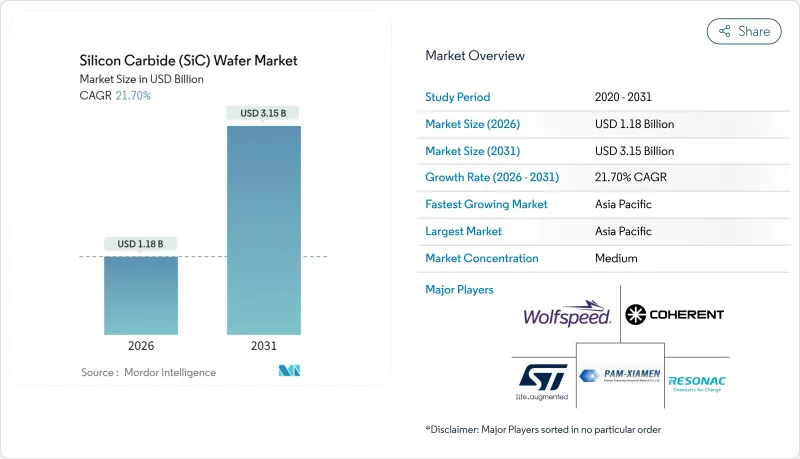
预计到 2026 年,碳化硅晶片市场价值将达到 11.8 亿美元,从 2025 年的 9.7 亿美元成长到 2031 年的 31.5 亿美元,2026 年至 2031 年的复合年增长率为 21.7%。
这一成长轨迹得益于汽车产业向800V汽车平臺的转型、工业电力电子领域对宽能带隙装置日益增长的需求,以及政府为支持新建生产线而提供的激励措施。晶体生长产量比率的稳定提升、8吋基板供应量的增加以及对高效快速充电基础设施需求的不断增长,正在推动市场进一步扩张。到2024年,亚太地区将占据最大的市场份额,其垂直整合的生态系统将持续吸引上下游投资。儘管资本密集度仍然是关键的竞争因素,但那些掌握了缺陷减少、晶圆尺寸缩小和内部供应链管理技术的公司,将有望抓住碳化硅晶圆市场的下一波需求浪潮。碳化硅晶圆在高温高频工作环境下性能优于传统硅晶圆。
全球碳化硅(SiC)晶圆市场趋势及洞察
提高电动车渗透率并向 800V汽车平臺过渡
汽车製造商已透过特斯拉 Model S Plaid、现代 IONIQ 5 和起亚 EV6 等车款展示了大规模800V 系统的应用。虽然这些高压架构显着缩短了充电时间至 20 分钟以内,但它们需要能够承受高热应力和电应力的功率 MOSFET。碳化硅满足这些要求,其电场强度是硅的 10 倍,导热係数是硅的 3 倍,从而推动了驱动逆变器和车载充电器对碳化硅的需求。虽然豪华车市场最初采用了这项技术,但晶圆成本的下降和供应链的成熟正在加速其在主流电动车平台上的应用,进一步提升了碳化硅晶圆市场作为下一代移动出行关键基础技术的重要性。
800V充电基础设施的快速扩张
为了最大限度地减少350kW充电站的转换损耗,充电网路营运商选择了碳化硅(SiC)作为晶圆材料。 Electrify Americas的主充电站整合了基于SiC的整流器和DC-DC模组,与硅相比,实现了更高的功率密度和更低的散热。欧洲充电走廊供应商IONITY也采取了类似的策略,从而形成了一个良性循环的供需关係,促使汽车製造商采用800V平台。最终形成了一个涵盖车辆、充电器和并联型设备的生态系统,在提高晶圆需求的同时,透过提高能源效率降低成本,从而降低了网路营运商的整体拥有成本(TCO)。
200mm基板的供应限制
200毫米晶锭的生长週期通常超过200小时,且缺陷密度高于150毫米晶锭,这限制了汽车级基板的供应。产量比率下降推高了晶圆的平均售价(ASP),并减缓了设计到更大直径的转变。儘管製造商正在投资先进的原位监测技术和晶种优化以弥补缺口,但短期供不应求仍然抑制着碳化硅晶圆的市场出货量成长,尤其是对于要求严格品质标准的汽车製造商。
细分市场分析
2025年,6吋晶圆占据了碳化硅晶圆市场53.75%的份额。由于每片晶圆的装置数量和晶粒折旧免税额较高,这种传统尺寸已成为大规模生产的标准。然而,预计到2031年,8吋晶圆的复合年增长率将达到28.6%,这进一步巩固了其在牵引和光伏逆变器领域每安培成本的优势。目前,8吋晶圆的资本支出仍然很高。一台用于200毫米晶体的高PVT炉造价为1500万至2000万美元,而6吋晶圆的PVT炉造价仅为800万至1200万美元。但是,8吋晶圆的晶粒产量可达6吋晶圆的2.2倍,随着产量比率的提高,成本曲线将更加紧凑。随着规模经济效应的显现,8吋基板碳化硅晶圆市场预计将成为日益重要的收入来源。
截至2024年,200毫米晶圆的产量比率比同等尺寸的6吋晶圆低15-20%,但优化加热区设计与缺陷减少分析的投资已缩小了这一差距。汽车和可再生能源整合公司已启动200毫米晶圆的认证项目,这预示着一旦大规模生产供应稳定,200毫米晶圆将被更广泛地采用。随着研发重心转向高压汽车或电网模组,小于4吋的晶圆尺寸持续下降,而大于12吋的原型产品仍仅限于学术界。因此,成功实现8吋晶圆的规模化生产标誌着碳化硅晶圆市场的关键转折点。
到2025年,N型导电硅晶片将占据碳化硅硅片市场68.12%的份额。其低电阻率和稳定的掺杂分布使其成为功率MOSFET、二极体和肖特基元件的关键材料。半绝缘基板传统上是小众市场,但预计到2031年将以23.6%的复合年增长率成长,这主要得益于5G基地台、雷达和卫星有效载荷中射频和微波技术的应用。网路技术的进步和国防电子技术的发展需要高纯度、电隔离的晶格结构来降低吉赫频段的寄生电容,从而推动了半绝缘碳化硅硅片市场的发展。
随着晶圆直径的增加,製造商不断改进生长后退火和补偿掺杂技术,以提高电阻率均匀性。航太和通讯公司由于其优异的热处理性能,更倾向于使用半绝缘晶圆製造GaN-on-SiC HEMT装置。因此,能够确保高导热性、电绝缘性和卓越射频性能的晶圆在竞争格局中变得愈发重要。这一趋势凸显了半绝缘碳化硅在下一代装置架构发展中将扮演的重要角色。
碳化硅 (SiC) 晶圆市场按晶圆直径(小于 4 吋、大于 4 吋)、导电类型(N 型导电、半绝缘)、应用领域(电力电子、射频元件等)、终端用户产业(汽车及电动车、可再生能源及储能等)、晶体生长技术(PVT、CVD 等)及地区进行细分。市场预测以美元以金额为准(USD) 为单位。
区域分析
北美位居第二,这得益于回流激励政策和完善的电动车生态系统。 Wolfspeed位于莫霍克谷的晶圆厂开始量产200毫米晶圆,特斯拉检验了大规模碳化硅牵引逆变器,推动了区域供应协议的达成。安森美半导体决定投资高达20亿美元在捷克共和国建造端到端的碳化硅生产系统,不仅为欧洲汽车製造商提供了更多选择,也使其在美国保持了技术领先地位。同时,罗姆和SK Siltron透过生产高品质基板保持了技术优势,使其能够在价格下行压力下维持高价位。
由于回流激励政策和强大的电动车生态系统,北美保持了第二的位置。 Wolfspeed位于莫霍克谷的晶圆厂已开始量产200毫米晶圆,特斯拉大规模SiC牵引逆变器的检验促成了区域供应协议的达成。安森美半导体(ON Semiconductor)正在投资高达20亿美元,在捷克共和国建造端到端的SiC生产能力,这不仅为欧洲汽车製造商提供了更多选择,也保持了美国的技术优势。
欧洲在绿色交易电气化政策和强大的汽车产业基础的推动下取得了长足进步。英飞凌扩大了在奥地利和德国的晶圆产能,以支援保时捷和奥迪的800V平台,并将品质和可靠性置于成本最低之上。意法半导体扩建了位于卡塔尼亚的工厂,为符合欧盟半导体自给自足目标的区域供应链奠定了基础。碳化硅晶圆市场仍对价格敏感,但欧洲买家更重视汽车级可追溯性和严格的缺陷控制标准。
其他福利:
- Excel格式的市场预测(ME)表
- 3个月的分析师支持
目录
第一章 引言
- 研究假设和市场定义
- 调查范围
第二章调查方法
第三章执行摘要
第四章 市场情势
- 市场概览
- 市场驱动因素
- 电动车日益普及以及向 800V汽车平臺的过渡
- 800V充电基础设施快速发展
- 碳化硅在高温和高频性能方面优于硅
- 政府对宽能带隙晶圆厂的奖励措施
- 中国垂直整合型碳化硅供应链的崛起
- 创新 200mm 体生长技术的进步可降低缺陷密度
- 市场限制
- 200mm基板供应限制
- 包装引起的热机械应力
- 资本密集型晶体生长设备
- 碳化硅切割废弃物的回收利用问题
- 产业价值链分析
- 监管环境
- 技术展望
- 宏观经济因素的影响
- 波特五力分析
- 供应商的议价能力
- 买方的议价能力
- 新进入者的威胁
- 替代品的威胁
- 竞争对手之间的竞争
第五章 市场规模与成长预测
- 依晶圆直径
- 小于4英寸
- 6吋
- 8吋
- 12吋或以上
- 依导电类型
- N型导电性
- 半绝缘
- 透过使用
- 电力电子
- 高频装置
- 光电子学和发光二极体
- 其他用途
- 按最终用途行业划分
- 汽车和电动车
- 可再生能源和储能
- 电讯
- 工业马达驱动装置和不断电系统(UPS)
- 航太/国防
- 其他终端用户产业
- 透过晶体生长技术
- 物理蒸气传输(PVT)
- 化学气相沉积(CVD)
- 改良的莱利昇华法
- 其他技术
- 按地区
- 北美洲
- 美国
- 加拿大
- 南美洲
- 巴西
- 阿根廷
- 南美洲其他地区
- 欧洲
- 德国
- 法国
- 英国
- 义大利
- 西班牙
- 其他欧洲地区
- 亚太地区
- 中国
- 日本
- 韩国
- 台湾
- 印度
- 亚太其他地区
- 中东和非洲
- 中东
- 沙乌地阿拉伯
- 阿拉伯聯合大公国
- 其他中东地区
- 非洲
- 南非
- 奈及利亚
- 其他非洲地区
- 中东
- 北美洲
第六章 竞争情势
- 市场集中度
- 策略趋势
- 市占率分析
- 公司简介
- Wolfspeed Inc.
- Coherent Corp.
- Xiamen Powerway Advanced Material Co., Ltd.
- STMicroelectronics NV
- Resonac Holdings Corporation
- Atecom Technology Co., Ltd.
- SK Siltron Co., Ltd.
- SiCrystal GmbH
- Tankeblue Semiconductor Co., Ltd.
- Semiconductor Wafer Inc.
- GlobalWafers Co., Ltd.
- Sanan Optoelectronics Co., Ltd.
- ROHM Co., Ltd.
- Infineon Technologies AG
- onsemi Corporation
- Mitsubishi Electric Corporation
- Hebei Synlight Crystal Co., Ltd.
- Guangdong TySiC Semiconductor Co., Ltd.
- EpiWorld International Co., Ltd.
- Hench Semiconductor Co., Ltd.
- TYSTC Semiconductor Co., Ltd.
- ProChip Moissic Technologies Inc.
- Dow Silicon Carbide LLC
- Fraunhofer IISB(SiC Foundry)
- Nippon Steel & Sumitomo Metal SiC Materials Co., Ltd.
- LPE SpA
第七章 市场机会与未来展望
The silicon carbide wafer market size in 2026 is estimated at USD 1.18 billion, growing from 2025 value of USD 0.97 billion with 2031 projections showing USD 3.15 billion, growing at 21.7% CAGR over 2026-2031.
The growth trajectory is supported by the automotive industry's migration to 800 V vehicle platforms, wide-band-gap adoption in industrial power electronics, and government incentives that underwrite new fabrication lines. Steadily improving crystal-growth yields, wider availability of 8-inch substrates, and rising demand for efficient fast-charging infrastructure further underpin expansion. Asia-Pacific held the largest regional share in 2024, and its vertically integrated ecosystem continues to attract upstream and downstream investments. Capital intensity remains a key competitive filter, yet companies that master defect reduction, wafer scaling, and internal supply chains are positioned to capture the next wave of demand as the silicon carbide wafer market outperforms conventional silicon in high-temperature and high-frequency operating environments.
Global Silicon Carbide (SiC) Wafer Market Trends and Insights
Rising EV Penetration and Shift Toward 800 V Vehicle Platforms
Automakers demonstrated large-scale 800 V system adoption through models such as Tesla's Model S Plaid, Hyundai's IONIQ 5, and Kia's EV6. These high-voltage architectures reduced charging times well below 20 minutes yet demanded power MOSFETs capable of withstanding elevated thermal and electrical stress. Silicon carbide meets these thresholds due to a ten-fold higher critical electric field and three-fold higher thermal conductivity than silicon, which magnifies demand in traction inverters and onboard chargers. Luxury and premium segments adopted the technology first, but falling wafer costs and maturing supply chains now accelerate diffusion into mainstream EV platforms, reinforcing the silicon carbide wafer market as an essential enabler of next-generation mobility.
Rapid Build-out of 800 V Charging Infrastructure
Charging network operators selected silicon carbide to minimise conversion losses in 350 kW stations. Electrify America's flagship sites integrated SiC-based rectifiers and DC-DC modules, achieving higher power density and lower heat dissipation compared with silicon. European corridor provider IONITY followed a similar path, creating a supply-demand flywheel that encourages automakers to embrace 800 V platforms. The resulting ecosystem, spanning vehicles, chargers, and grid-interfacing equipment, ramps up wafer volumes while compressing total ownership cost for network operators through energy-efficiency savings.
Limited Availability of 200 mm Substrates
Crystal-growth cycles for 200 mm boules often exceeded 200 hours and yielded higher defect densities than 150 mm equivalents, constraining the supply of automotive-grade substrates. Yield penalties elevated wafer ASPs and delayed design transitions to larger diameters. Fabricators invested in advanced in-situ monitoring and seed-crystal optimisation to close the gap, yet near-term shortages continue to cap silicon carbide wafer market shipment growth, especially for carmakers that require stringent quality thresholds.
Other drivers and restraints analyzed in the detailed report include:
- High-Temperature, High-Frequency Performance Advantages over Silicon
- Government Incentives for Wide-Band-Gap Fabs
- Packaging-Induced Thermo-Mechanical Stress
For complete list of drivers and restraints, kindly check the Table Of Contents.
Segment Analysis
The silicon carbide wafer market recorded 6-inch substrates at 53.75% share in 2025. Device counts per wafer and depreciation per die positioned this legacy diameter as the volume benchmark. However, 8-inch substrates are forecast to expand at a 28.6% CAGR through 2031, underscoring the cost-per-ampere advantage for traction inverters and PV inverters. Equipment investments remain high-PVT furnaces for 200 mm crystals cost USD 15-20 million versus USD 8-12 million for 6-inch. Nonetheless, each 8-inch wafer can deliver up to a 2.2-fold increase in die output, tightening the cost curve as yields improve. The silicon carbide wafer market size for 8-inch substrates is projected to command an increasingly large revenue pool as scale economies kick in.
Although yield rates lagged 6-inch equivalents by 15-20% in 2024, investment in hot-zone design optimisation and defect-reduction analytics narrowed the gap. Automotive and renewable energy integrators began qualification programs for 200 mm die, signalling broader acceptance once volume supply stabilises. less than 4-inch formats continued to decline as R&D moves toward high-voltage automotive or grid modules, while above 12-inch prototypes remained confined to academia. Successful scale-up to 8-inch thus stands as the pivotal inflection point for the silicon carbide wafer market.
N-type conductive wafers accounted for 68.12% of the silicon carbide wafer market share in 2025. Their low resistivity and stable dopant profiles made them indispensable for power MOSFETs, diodes, and Schottky devices. Semi-insulating substrates, although historically niche, are poised for 23.6% CAGR growth to 2031, driven by RF and microwave adoption in 5G base stations, radar, and satellite payloads. The silicon carbide wafer market size allocated to semi-insulating material is set to swell as network densification and defense electronics demand pure, electrically isolated lattices to limit parasitic capacitance at gigahertz frequencies.
Producers continue to refine post-growth annealing and compensation-doping techniques to lift resistivity uniformity across larger diameters. Aerospace and telecommunications firms favour semi-insulating wafers for GaN-on-SiC HEMTs that deliver superior thermal handling. As a result, the competitive landscape increasingly values substrates that ensure high thermal conductivity, electrical isolation, and superior RF performance. This trend highlights semi-insulating silicon carbide as a pivotal player in the evolution of next-generation device architectures.
Silicon Carbide (SiC) Wafer Market is Segmented by Wafer Diameter (less Than 4 Inch, and More), Conductivity Type (N-Type Conductive and Semi-Insulating), Application (Power Electronics, RF Devices, and More), End-Use Industry (Automotive and Electric Vehicles, Renewable Energy and Storage, and More), Crystal-Growth Technology (PVT, CVD, and More), and Geography. The Market Forecasts are Provided in Terms of Value (USD).
Geography Analysis
North America ranked second, bolstered by reshoring incentives and a deep EV ecosystem. Wolfspeed's Mohawk Valley fab ramped 200 mm wafers, and Tesla validated large-scale SiC traction inverters, spurring regional supply agreements. OnSemi committed up to USD 2 billion to establish end-to-end SiC production in the Czech Republic, providing optionality for European auto OEMs while retaining US technology leadership.chnology leadership through premium substrate production at ROHM and SK Siltron, preserving high ASPs despite down-price pressure.
North America ranked second, bolstered by reshoring incentives and a deep EV ecosystem. Wolfspeed's Mohawk Valley fab ramped 200 mm wafers, and Tesla validated large-scale SiC traction inverters, spurring regional supply agreements. OnSemi committed up to USD2 billion to establish end-to-end SiC production in the Czech Republic, providing optionality for European auto OEMs while retaining US technology leadership.
Europe advanced on the back of Green Deal electrification policies and a strong automotive base. Infineon expanded wafer output in Austria and Germany to serve Porsche and Audi 800 V platforms, emphasising quality and reliability over lowest cost. STMicroelectronics scaled its Catania site, anchoring a local supply chain that aligned with EU semiconductor sovereignty goals. Although the silicon carbide wafer market remained price sensitive, European buyers valued automotive-grade traceability and tight defect specifications.
- Wolfspeed Inc.
- Coherent Corp.
- Xiamen Powerway Advanced Material Co., Ltd.
- STMicroelectronics N.V.
- Resonac Holdings Corporation
- Atecom Technology Co., Ltd.
- SK Siltron Co., Ltd.
- SiCrystal GmbH
- Tankeblue Semiconductor Co., Ltd.
- Semiconductor Wafer Inc.
- GlobalWafers Co., Ltd.
- Sanan Optoelectronics Co., Ltd.
- ROHM Co., Ltd.
- Infineon Technologies AG
- onsemi Corporation
- Mitsubishi Electric Corporation
- Hebei Synlight Crystal Co., Ltd.
- Guangdong TySiC Semiconductor Co., Ltd.
- EpiWorld International Co., Ltd.
- Hench Semiconductor Co., Ltd.
- TYSTC Semiconductor Co., Ltd.
- ProChip Moissic Technologies Inc.
- Dow Silicon Carbide LLC
- Fraunhofer IISB (SiC Foundry)
- Nippon Steel & Sumitomo Metal SiC Materials Co., Ltd.
- LPE S.p.A.
Additional Benefits:
- The market estimate (ME) sheet in Excel format
- 3 months of analyst support
TABLE OF CONTENTS
1 INTRODUCTION
- 1.1 Study Assumptions and Market Definition
- 1.2 Scope of the Study
2 RESEARCH METHODOLOGY
3 EXECUTIVE SUMMARY
4 MARKET LANDSCAPE
- 4.1 Market Overview
- 4.2 Market Drivers
- 4.2.1 Rising EV penetration and shift toward 800-V vehicle platforms
- 4.2.2 Rapid build-out of 800 V charging infrastructure
- 4.2.3 High-temperature, high-frequency performance advantages over Si
- 4.2.4 Government incentives for wide-band-gap fabs
- 4.2.5 Emergence of vertically-integrated SiC supply chains in China
- 4.2.6 Novel 200 mm bulk-growth breakthroughs lowering defect density
- 4.3 Market Restraints
- 4.3.1 Limited availability of 200 mm substrates
- 4.3.2 Packaging-induced thermo-mechanical stress
- 4.3.3 Capital-intensive crystal-growth equipment
- 4.3.4 Recycling challenges for SiC kerf waste
- 4.4 Industry Value Chain Analysis
- 4.5 Regulatory Landscape
- 4.6 Technological Outlook
- 4.7 Impact of Macroeconomic Factors
- 4.8 Porter's Five Forces Analysis
- 4.8.1 Bargaining Power of Suppliers
- 4.8.2 Bargaining Power of Buyers
- 4.8.3 Threat of New Entrants
- 4.8.4 Threat of Substitutes
- 4.8.5 Intensity of Competitive Rivalry
5 MARKET SIZE AND GROWTH FORECASTS (VALUE)
- 5.1 By Wafer Diameter
- 5.1.1 less than 4 inch
- 5.1.2 6 inch
- 5.1.3 8 inch
- 5.1.4 above 12 inch
- 5.2 By Conductivity Type
- 5.2.1 N-Type Conductive
- 5.2.2 Semi-insulating
- 5.3 By Application
- 5.3.1 Power Electronics
- 5.3.2 Radio-Frequency Devices
- 5.3.3 Optoelectronics and LED
- 5.3.4 Other Applications
- 5.4 By End-use Industry
- 5.4.1 Automotive and Electric Vehicles
- 5.4.2 Renewable Energy and Storage
- 5.4.3 Telecommunications
- 5.4.4 Industrial Motor Drives and UPS
- 5.4.5 Aerospace and Defense
- 5.4.6 Other End-user Industries
- 5.5 By Crystal-Growth Technology
- 5.5.1 Physical Vapor Transport (PVT)
- 5.5.2 Chemical Vapor Deposition (CVD)
- 5.5.3 Modified Lely Sublimation
- 5.5.4 Other Technologies
- 5.6 By Geography
- 5.6.1 North America
- 5.6.1.1 United States
- 5.6.1.2 Canada
- 5.6.2 South America
- 5.6.2.1 Brazil
- 5.6.2.2 Argentina
- 5.6.2.3 Rest of South America
- 5.6.3 Europe
- 5.6.3.1 Germany
- 5.6.3.2 France
- 5.6.3.3 United Kingdom
- 5.6.3.4 Italy
- 5.6.3.5 Spain
- 5.6.3.6 Rest of Europe
- 5.6.4 Asia-Pacific
- 5.6.4.1 China
- 5.6.4.2 Japan
- 5.6.4.3 South Korea
- 5.6.4.4 Taiwan
- 5.6.4.5 India
- 5.6.4.6 Rest of Asia-Pacific
- 5.6.5 Middle East and Africa
- 5.6.5.1 Middle East
- 5.6.5.1.1 Saudi Arabia
- 5.6.5.1.2 United Arab Emirates
- 5.6.5.1.3 Rest of Middle East
- 5.6.5.2 Africa
- 5.6.5.2.1 South Africa
- 5.6.5.2.2 Nigeria
- 5.6.5.2.3 Rest of Africa
- 5.6.5.1 Middle East
- 5.6.1 North America
6 COMPETITIVE LANDSCAPE
- 6.1 Market Concentration
- 6.2 Strategic Moves
- 6.3 Market Share Analysis
- 6.4 Company Profiles (includes Global level Overview, Market level overview, Core Segments, Financials as available, Strategic Information, Market Rank/Share for key companies, Products and Services, and Recent Developments)
- 6.4.1 Wolfspeed Inc.
- 6.4.2 Coherent Corp.
- 6.4.3 Xiamen Powerway Advanced Material Co., Ltd.
- 6.4.4 STMicroelectronics N.V.
- 6.4.5 Resonac Holdings Corporation
- 6.4.6 Atecom Technology Co., Ltd.
- 6.4.7 SK Siltron Co., Ltd.
- 6.4.8 SiCrystal GmbH
- 6.4.9 Tankeblue Semiconductor Co., Ltd.
- 6.4.10 Semiconductor Wafer Inc.
- 6.4.11 GlobalWafers Co., Ltd.
- 6.4.12 Sanan Optoelectronics Co., Ltd.
- 6.4.13 ROHM Co., Ltd.
- 6.4.14 Infineon Technologies AG
- 6.4.15 onsemi Corporation
- 6.4.16 Mitsubishi Electric Corporation
- 6.4.17 Hebei Synlight Crystal Co., Ltd.
- 6.4.18 Guangdong TySiC Semiconductor Co., Ltd.
- 6.4.19 EpiWorld International Co., Ltd.
- 6.4.20 Hench Semiconductor Co., Ltd.
- 6.4.21 TYSTC Semiconductor Co., Ltd.
- 6.4.22 ProChip Moissic Technologies Inc.
- 6.4.23 Dow Silicon Carbide LLC
- 6.4.24 Fraunhofer IISB (SiC Foundry)
- 6.4.25 Nippon Steel & Sumitomo Metal SiC Materials Co., Ltd.
- 6.4.26 LPE S.p.A.
7 MARKET OPPORTUNITIES AND FUTURE OUTLOOK
- 7.1 White-space and Unmet-need Assessment
 全球碳化硅晶圆抛光市场规模、份额、趋势和成长分析报告(2026-2034年)
 2026年全球碳化硅晶圆加工市场研究报告
 4吋SiC晶圆市场依产品类型、电压等级、纯度等级及应用划分,全球预测(2026-2032年)4吋和6吋SiC晶圆市场(按晶圆尺寸、晶体结构、掺杂类型、装置类型、通路和应用划分)-全球预测,2026-2032年6吋导电SiC晶圆市场(按应用、终端用户产业、多型、基板类型、外延层和掺杂类型划分),全球预测,2026-2032年8吋碳化硅晶圆市场(依晶圆类型、元件类型、掺杂类型、电阻率、表面光洁度和应用划分),全球预测,2026-2032年碳化硅晶圆市场按产品类型、晶圆直径、应用、通路和装置类型划分,全球预测(2026-2032年)碳化硅(SiC)晶圆和基板市场(按多型、晶圆直径、晶圆取向、晶圆类型和应用划分),全球预测,2026-2032年
 碳化硅晶片:全球市占率及排名、总收入及需求预测(2025-2031年)碳化硅抛光耗材:全球市占率排名、总销售额及需求预测(2025-2031年)