


 |
市场调查报告书
商品编码
1939642
介质蚀刻机:市场占有率分析、产业趋势与统计、成长预测(2026-2031)Dielectric Etchers - Market Share Analysis, Industry Trends & Statistics, Growth Forecasts (2026 - 2031) |
||||||
※ 本网页内容可能与最新版本有所差异。详细情况请与我们联繫。
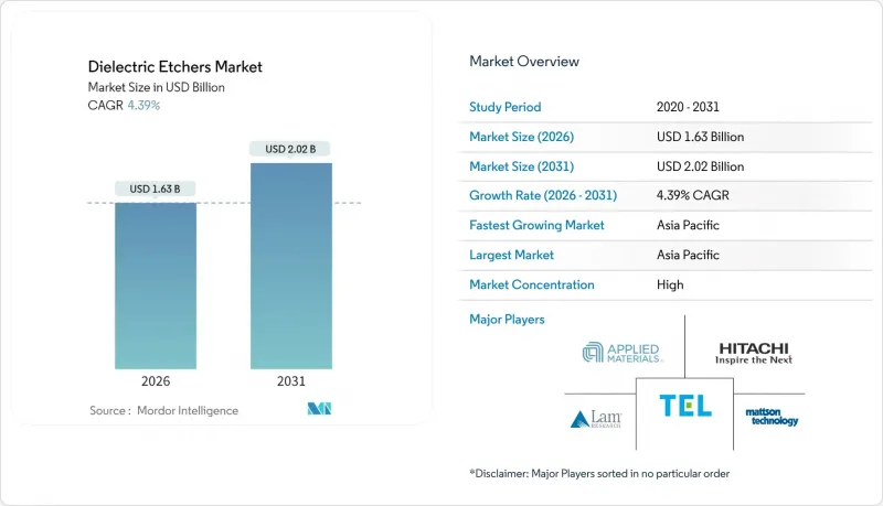
预计到 2026 年,介电蚀刻机市场规模将达到 16.3 亿美元,高于 2025 年的 15.6 亿美元,预计到 2031 年将达到 20.2 亿美元。
预计从 2026 年到 2031 年,其复合年增长率将达到 4.39%。
儘管装置需求放缓,但对7奈米以下製程原子级精度的需求不断增长、3D NAND快闪记忆体层数的增加以及先进封装中低介电常数材料的应用,都将使资本支出居高不下。随着环栅(GAA)逻辑和异构整合技术的进步缩短了设备更换週期,晶圆代工厂继续推动介电层蚀刻机市场的发展。从区域来看,倡议占了设备安装量的主导地位,但北美CHIPS法案资助的晶圆厂和欧盟的CHIPS计画正在重塑采购格局。拥有多材料製程技术和国内供应链的供应商最能掌握当前的设备更新换代浪潮,而原子层蚀刻(ALE)和低温等离子体模组等精度增强技术正在开闢新的差异化途径。
全球介电蚀刻机市场趋势与洞察
7奈米以下逻辑节点的普及
7nm及以下製程的量产增加了掩模数量并缩小了製程窗口,导致蚀刻步骤数量比10nm製程增加了40%至60%。 GaAs电晶体需要移除牺牲SiGe层,同时不能损坏高k层,这迫使晶圆厂以支援ALE(原子层蚀刻)的装置取代传统的蚀刻腔。台积电2025年的380亿至420亿美元资本支出将主要用于其2nm中试生产线,以确保高选择性介质模组的多年订单。随着製程节点的转换与封装技术的更新换代同步进行,设备更新周期将从五年缩短至三年,为介质蚀刻市场带来稳定的收入。能够与客户共同开发化学製程的设备製造商将享有优先供应商地位,从而加强市场进入门槛。
增加3D NAND的层数
在超过400层的堆迭结构中蚀刻64µm深的通道孔,需要接近100:1的长宽比控制,这对等离子体均匀性和副产物排放提出了更高的要求。东京电子计画于2025年推出低温蚀刻技术,可减少翘曲和变形,挑战Lam Research在记忆体蚀刻领域的统治地位。每增加32层,就需要重新设计蚀刻腔,这使得三星等NAND快闪记忆领导企业的更换週期长达18至24个月。这使得介质蚀刻设备市场能够受益于记忆体投资,即使在逻辑晶片需求疲软时期也能缓解收入波动。
蚀刻设备资本密集度高
最先进的介质腔造价在500万至800万美元之间,而ALE丛集的安装成本可能高达1200万至1500万美元。董事会层级的核准和长期租赁审查导致安装延迟6至12个月,尤其对于中小型IDM和特种晶圆厂而言更是如此。供应商正在推出模组化平台来应对这项挑战,这些平台共用射频、真空和晶圆处理子系统,将成本分摊到各个製程节点,但预算上限仍然使介质刻蚀机市场近期的成长放缓了70个基点。
细分市场分析
到2025年,二氧化硅仍将占据介电蚀刻机市场38.10%的份额,为成熟的逻辑电路和DRAM製程提供支持,在这些流程中,成本增长速度超过了性能增长速度。低介电常数材料用介电蚀刻机的市场规模预计将以468.12%的复合年增长率快速成长,这反映了人工智慧加速器对低电容基板的需求。
低介电常数材料的应用,需要采用避免碳损耗和铜腐蚀的等离子体化学工艺,这推动了多频射频技术的创新,而只有现有供应商才能实现大规模商业化。同时,氮化硅和新兴玻璃介质在隔离层和麵板级封装中扮演着独特的角色,对刻蚀选择性提出了前所未有的要求。为了满足这些多样化的需求,设备製造商必须整合原位终点计量技术和多重压力腔室,这推高了转换成本,并维持了介质蚀刻机市场的收入多样性。
反应离子蚀刻 (RIE) 仍将是成本敏感领域的领导技术,到 2025 年将占介电蚀刻机市场的 42.26%。然而,原子层蚀刻 (ALEC) 5.02% 的年增长率证实了其在 GAA 电晶体、3D NAND 和量子电路中的必然性。
製造商正在权衡产能损失和产量比率提升。试验数据显示,当采用原子层蚀刻 (ALE) 取代鳍片侧壁上的多步骤反应离子蚀刻 (RIE) 时,缺陷密度可降低 35% 至 45%。东京电子的低温 RIE 混合技术模糊了传统製程与 ALE 的界限,使晶圆厂能够在保持製程週期预算的同时,策略性地应用 ALE 技术。这种混合化正在使介质蚀刻机市场碎片化,为中型供应商开闢了空间,使其能够在微波等离子体和紫外线辅助製程等领域开闢新的市场。
区域分析
到2025年,亚太地区将占介质蚀刻机市场规模的64.51%,这主要得益于韩国记忆体产业和台湾逻辑产业丛集的强劲成长。光是中国大陆就贡献了Lam Research 42%的收入,但出口限制带来的不利影响迫使企业采取双重采购和在地化设备製造策略。日本、印度和新加坡等国政府正大力投资其后端产业生态系统,扩大了区域设备需求,使其超越了传统市场。
《北美晶片製造法案》(North American CHIPS Act)将在21个州投资超过330亿美元,用于支持建造四座新的巨型晶圆厂,每座晶圆厂都需要500多个介电腔室。国内含量条款将提高在美国拥有组装线的供应商的份额,从而促进全球晶片分配模式摆脱对任何单一地区的依赖。
欧洲正透过《欧盟晶片法案》推进自主采购,而德国和法国则吸引了许多大型记忆体和类比电路公司。儘管欧洲大陆的整体市场份额落后于亚洲,但由于自主采购模式推动了对综合工具套件(而非附加组件)需求的成长,其成长速度正在加快。这些变化共同作用,透过地理多元化的收入来源,在区域政策波动的情况下,稳定了介电蚀刻机市场。
其他福利:
- Excel格式的市场预测(ME)表
- 3个月的分析师支持
目录
第一章 引言
- 研究假设和市场定义
- 调查范围
第二章调查方法
第三章执行摘要
第四章 市场情势
- 市场概览
- 市场驱动因素
- 7奈米以下逻辑节点的普及
- 增加3D NAND的层数
- 先进封装中低介电常数材料的采用
- 对 5G/AI 晶片的需求不断增长
- 向原子层蚀刻(ALE)过渡
- 政府资助的晶圆厂在地化(晶片法案、欧盟晶片法案等)
- 市场限制
- 蚀刻设备资本密集度高
- 半导体资本投资的週期性
- 新型材料的製程复杂性
- 严格的氟碳化合物环境法规
- 产业价值链分析
- 监管环境
- 技术展望
- 波特五力分析
- 新进入者的威胁
- 供应商的议价能力
- 买方的议价能力
- 替代品的威胁
- 产业间竞争
第五章 市场规模与成长预测
- 透过介电材料
- 二氧化硅(SiO2)
- 氮化硅(Si3N4)
- 低介电常数绝缘体
- 高介电常数电介质
- 其他成分
- 透过技术
- 反应离子蚀刻(RIE)
- 感应耦合电浆(ICP)
- 原子层蚀刻(ALE)
- 微波电浆蚀刻
- 其他技术
- 按晶圆尺寸
- 150毫米或更小
- 200 mm
- 300 mm
- 超过450毫米
- 最终用户
- Pure Play Foundry
- 集成设备製造商(IDM)
- MEMS和感测器製造
- 研发及中试生产线
- 按地区
- 北美洲
- 南美洲
- 欧洲
- 亚太地区
- 中东和非洲
第六章 竞争情势
- 市场集中度
- 策略趋势
- 市占率分析
- 公司简介
- Applied Materials, Inc.
- Lam Research Corporation
- Tokyo Electron Limited
- Hitachi High-Tech Corporation
- ASM International NV
- NAURA Technology Group Co., Ltd.
- Advanced Micro-Fabrication Equipment Inc. China(AMEC)
- SPTS Technologies Ltd.(KLA Corporation)
- Plasma-Therm LLC
- Oxford Instruments plc(Plasma Technology)
- Samco Inc.
- ULVAC, Inc.
- EBARA Corporation
- Dongshin Microelectronics Co., Ltd.
- Beijing Sevenstar Electronics Co., Ltd.
- Mattson Technology, Inc.
- Veeco Instruments Inc.
- Nordson MARCH(Nordson Corporation)
- Trion Technology, Inc.
- Corial SAS
- Plasma Etch, Inc.
- Diener Electronic GmbH and Co. KG
- PVA TePla AG
- Tokuda Seimitsu(Accretech)
- Shenzhen Ideal Energy Equipment Co., Ltd.
第七章 市场机会与未来展望
The dielectric etchers market size in 2026 is estimated at USD 1.63 billion, growing from 2025 value of USD 1.56 billion with 2031 projections showing USD 2.02 billion, growing at 4.39% CAGR over 2026-2031.
Rising atomic-layer precision needs at sub-7 nm, escalating 3D NAND layer counts and low-k dielectric adoption in advanced packaging keep capital spending elevated even when device demand cools. Foundries continue to drive the dielectric etchers market as gate-all-around (GAA) logic and heterogeneous integration shorten equipment replacement cycles. Regionally, Asia Pacific dominates installations, but CHIPS Act-funded fabs in North America and EU Chips initiatives are reshaping procurement geography. Vendors with multi-material process know-how and domestic supply chains are best positioned to capture the current wave of re-tooling, while precision enhancements such as atomic-layer etching (ALE) and cryogenic plasma modules create new differentiation avenues.
Global Dielectric Etchers Market Trends and Insights
Proliferation of Sub-7 nm Logic Nodes
Sub-7 nm production raises mask counts and shrinks process windows, pushing etch step totals 40-60% higher than 10 nm flows. GAA transistors require sacrificial SiGe removal without scarring high-k layers, forcing fabs to swap legacy chambers for ALE-ready tools. TSMC's USD 38-42 billion 2025 capex focuses on 2 nm pilot lines, locking in multi-year orders for high-selectivity dielectric modules. Because node migrations now coincide with packaging overhauls, tool refreshes happen on a three-year rather than five-year cadence, anchoring steady revenue for the dielectric etchers market. Equipment makers that can co-develop chemistries with customers enjoy preferred-supplier status, reinforcing market entry barriers.
3D NAND Layer-Count Escalation
Etching 64 µm-deep channel holes through above 400-layer stacks demands aspect-ratio control near 100:1, pressuring plasma uniformity and by-product evacuation. Cryogenic etch launched by Tokyo Electron in 2025 mitigates bowing and twisting, answering Lam Research's hold in memory etch. Each 32-layer leap forces chamber redesigns, driving an 18-24 month replacement cycle at Samsung and other NAND leaders. The dielectric etchers market therefore benefits from memory spending even during logic lulls, buffering revenue volatility.
High Capital Intensity of Etch Tools
State-of-the-art dielectric chambers cost USD 5-8 million, and ALE clusters can top USD 12-15 million installed. Board-level approvals and extended leasing reviews delay installs 6-12 months, especially at smaller IDMs and specialty fabs. Vendors respond with modular platforms that share RF, vacuum, and wafer-handling subsystems to spread expenses across process nodes, yet budget ceilings still trim the near-term dielectric etchers market expansion rate by 70 basis points.
Other drivers and restraints analyzed in the detailed report include:
- Low-k Dielectric Adoption in Advanced Packaging
- Rising 5G/AI Chip Volumes
- Semiconductor CAPEX Cyclicality
For complete list of drivers and restraints, kindly check the Table Of Contents.
Segment Analysis
Silicon dioxide retained 38.10% dielectric etchers market share in 2025, anchoring mature logic and DRAM flows where cost trumps performance. The dielectric etchers market size for low-k materials is projected to balloon alongside a 468.12% CAGR, reflecting AI accelerators' need for minimal capacitance substrates.
Low-k adoption compels plasma chemistries that avoid carbon depletion and copper corrosion, spurring multi-frequency RF innovations that established vendors alone can commercialize at scale. Simultaneously, silicon nitride and emerging glass dielectrics hold niche roles for barrier and panel-level packaging, demanding etch selectivity previously unseen. This broadening palette obliges toolmakers to bundle in situ endpoint metrology and multi-pressure chambers, reinforcing switching costs and sustaining revenue diversity across the dielectric etchers market.
Reactive-ion etching commanded 42.26% of the dielectric etchers market in 2025 and remains the workhorse for cost-sensitive layers. However, ALE's 5.02% annual growth underscores its inevitability for GAA, 3D NAND and quantum circuits.
Manufacturers weigh throughput penalties against yield gains; pilot data show defect-density cuts of 35-45% when ALE replaces multi-step RIE on fin sidewalls. Tokyo Electron's cryogenic RIE hybrid blurs boundaries, letting fabs phase-in ALE tactically while protecting cycle-time budgets. Such hybridization keeps the dielectric etchers market fragmented, enabling mid-tier suppliers to carve out niches in microwave plasma or UV-assisted processes.
The Global Dielectric Etchers Market Report is Segmented by Dielectric Material (Silicon Dioxide, Silicon Nitride, and More), Technology (Reactive-Ion Etching, Inductively-Coupled Plasma, and More), Wafer Size (less Than 150mm, 200mm, 300mm, and More), End User (Pure-Play Foundries, Idms, MEMS and Sensor Fabs, and R&D and Pilot Lines), and Geography. The Market Forecasts are Provided in Terms of Value (USD).
Geography Analysis
Asia Pacific accounted for 64.51% of dielectric etchers market size in 2025 on the strength of Korean memory and Taiwanese logic clusters. China alone delivered 42% of Lam Research's revenue, yet export-control headwinds compel dual-sourcing and localized toolmaking. Governments across Japan, India and Singapore fund backend ecosystems, widening regional tool demand beyond legacy hubs.
North America's CHIPS Act disperses over USD 33 billion across 21 states, underwriting four green-field mega-fabs that each require more than 500 dielectric chambers. Domestic sourcing clauses open share for suppliers with U.S. assembly lines, nudging global allocation away from single-region dependence.
Europe pursues sovereignty via the EU Chips Act, with Germany and France courting memory and analog giants. Though the continent's aggregate share trails Asia, growth rates accelerate as sovereign procurement pushes comprehensive tool suites rather than add-ons. These shifts collectively steady the dielectric etchers market by diversifying geographic revenue streams against regional policy shocks.
- Applied Materials, Inc.
- Lam Research Corporation
- Tokyo Electron Limited
- Hitachi High-Tech Corporation
- ASM International N.V.
- NAURA Technology Group Co., Ltd.
- Advanced Micro-Fabrication Equipment Inc. China (AMEC)
- SPTS Technologies Ltd. (KLA Corporation)
- Plasma-Therm LLC
- Oxford Instruments plc (Plasma Technology)
- Samco Inc.
- ULVAC, Inc.
- EBARA Corporation
- Dongshin Microelectronics Co., Ltd.
- Beijing Sevenstar Electronics Co., Ltd.
- Mattson Technology, Inc.
- Veeco Instruments Inc.
- Nordson MARCH (Nordson Corporation)
- Trion Technology, Inc.
- Corial SAS
- Plasma Etch, Inc.
- Diener Electronic GmbH and Co. KG
- PVA TePla AG
- Tokuda Seimitsu (Accretech)
- Shenzhen Ideal Energy Equipment Co., Ltd.
Additional Benefits:
- The market estimate (ME) sheet in Excel format
- 3 months of analyst support
TABLE OF CONTENTS
1 INTRODUCTION
- 1.1 Study Assumptions and Market Definition
- 1.2 Scope of the Study
2 RESEARCH METHODOLOGY
3 EXECUTIVE SUMMARY
4 MARKET LANDSCAPE
- 4.1 Market Overview
- 4.2 Market Drivers
- 4.2.1 Proliferation of sub-7 nm logic nodes
- 4.2.2 3D NAND layer-count escalation
- 4.2.3 Low-k dielectric adoption in advanced packaging
- 4.2.4 Rising 5G/AI chip volumes
- 4.2.5 Transition to atomic-layer etching (ALE)
- 4.2.6 Government-funded fab localization (CHIPS Act, EU Chips, etc.)
- 4.3 Market Restraints
- 4.3.1 High capital intensity of etch tools
- 4.3.2 Semiconductor CAPEX cyclicality
- 4.3.3 Process complexity with novel materials
- 4.3.4 Stringent F-gas environmental regulations
- 4.4 Industry Value Chain Analysis
- 4.5 Regulatory Landscape
- 4.6 Technological Outlook
- 4.7 Porter's Five Forces Analysis
- 4.7.1 Threat of New Entrants
- 4.7.2 Bargaining Power of Suppliers
- 4.7.3 Bargaining Power of Buyers
- 4.7.4 Threat of Substitutes
- 4.7.5 Industry Rivalry
5 MARKET SIZE AND GROWTH FORECASTS (VALUE)
- 5.1 By Dielectric Material
- 5.1.1 Silicon Dioxide (SiO2)
- 5.1.2 Silicon Nitride (Si3N4)
- 5.1.3 Low-k Dielectrics
- 5.1.4 High-k Dielectrics
- 5.1.5 Other Materials
- 5.2 By Technology
- 5.2.1 Reactive-Ion Etching (RIE)
- 5.2.2 Inductively-Coupled Plasma (ICP)
- 5.2.3 Atomic-Layer Etching (ALE)
- 5.2.4 Microwave Plasma Etching
- 5.2.5 Other Technologies
- 5.3 By Wafer Size
- 5.3.1 less than or equal to 150 mm
- 5.3.2 200 mm
- 5.3.3 300 mm
- 5.3.4 above 450 mm
- 5.4 By End User
- 5.4.1 Pure-play Foundries
- 5.4.2 Integrated Device Manufacturers (IDMs)
- 5.4.3 MEMS and Sensor Fabs
- 5.4.4 R&D and Pilot Lines
- 5.5 By Geography
- 5.5.1 North America
- 5.5.2 South America
- 5.5.3 Europe
- 5.5.4 Asia Pacific
- 5.5.5 Middle East and Africa
6 COMPETITIVE LANDSCAPE
- 6.1 Market Concentration
- 6.2 Strategic Moves
- 6.3 Market Share Analysis
- 6.4 Company Profiles {(includes Global level Overview, Market level overview, Core Segments, Financials as available, Strategic Information, Market Rank/Share for key companies, Products and Services, and Recent Developments)}
- 6.4.1 Applied Materials, Inc.
- 6.4.2 Lam Research Corporation
- 6.4.3 Tokyo Electron Limited
- 6.4.4 Hitachi High-Tech Corporation
- 6.4.5 ASM International N.V.
- 6.4.6 NAURA Technology Group Co., Ltd.
- 6.4.7 Advanced Micro-Fabrication Equipment Inc. China (AMEC)
- 6.4.8 SPTS Technologies Ltd. (KLA Corporation)
- 6.4.9 Plasma-Therm LLC
- 6.4.10 Oxford Instruments plc (Plasma Technology)
- 6.4.11 Samco Inc.
- 6.4.12 ULVAC, Inc.
- 6.4.13 EBARA Corporation
- 6.4.14 Dongshin Microelectronics Co., Ltd.
- 6.4.15 Beijing Sevenstar Electronics Co., Ltd.
- 6.4.16 Mattson Technology, Inc.
- 6.4.17 Veeco Instruments Inc.
- 6.4.18 Nordson MARCH (Nordson Corporation)
- 6.4.19 Trion Technology, Inc.
- 6.4.20 Corial SAS
- 6.4.21 Plasma Etch, Inc.
- 6.4.22 Diener Electronic GmbH and Co. KG
- 6.4.23 PVA TePla AG
- 6.4.24 Tokuda Seimitsu (Accretech)
- 6.4.25 Shenzhen Ideal Energy Equipment Co., Ltd.
7 MARKET OPPORTUNITIES AND FUTURE OUTLOOK
- 7.1 White-space and Unmet-Need Assessment
 半导体绝缘薄膜蚀刻设备市场报告:按类型、应用和地区划分 2026-2034 年
 介质蚀刻设备市场:依技术、设备类型、晶圆尺寸、最终用户和应用划分-2026-2032年全球市场预测
 离子束蚀刻系统市场:策略性洞察与预测(2026-2031年)全球蚀刻用硅元件市场(依技术类型、应用、晶圆直径、终端用户产业及销售管道)预测(2026-2032年)硅环和硅电极蚀刻市场:依产品类型、材料类型、应用、最终用途产业和销售管道划分,全球预测,2026-2032年硅蚀刻组件市场(依产品类型、晶圆直径、掺杂类型、晶体取向和应用划分),全球预测,2026-2032年
 氢基半导体蚀刻市场分析及预测(至2035年):依类型、产品类型、服务、技术、组件、应用、材料类型、製程、最终用户、设备划分
 半导体蚀刻设备:市场占有率分析、产业趋势与统计、成长预测(2026-2031)
 2026年全球蚀刻机市场报告2026年全球半导体蚀刻设备市场报告