


 |
市场调查报告书
商品编码
1939711
半导体蚀刻设备:市场占有率分析、产业趋势与统计、成长预测(2026-2031)Semiconductor Etch Equipment - Market Share Analysis, Industry Trends & Statistics, Growth Forecasts (2026 - 2031) |
||||||
※ 本网页内容可能与最新版本有所差异。详细情况请与我们联繫。
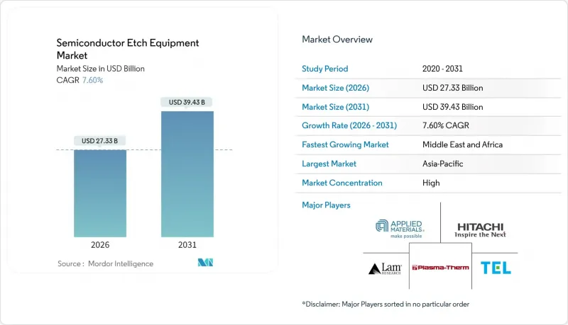
预计半导体蚀刻设备市场将从 2025 年的 254 亿美元成长到 2026 年的 273.3 亿美元,到 2031 年将达到 394.3 亿美元,2026 年至 2031 年的复合年增长率为 7.60%。
这一成长反映了对先进製程节点的持续资本投资、环栅电晶体的加速普及以及异质整合技术的广泛部署。人工智慧工作负载的不断增长、电动车产量的扩大以及政府补贴计划持续扩大已安装设备的潜在市场规模,而持续的氦气短缺和出口管制限制则影响着投资时机。儘管逻辑和微处理器代工厂仍然是设备需求量最大的客户,占据了最大的出货量份额,但随着资料中心营运商对更高频宽和更高能源效率的需求,高频宽记忆体和先进封装生产线的出货量成长最为迅速。虽然原子层蚀刻平台的收入成长最为显着,但由于其高吞吐量和化学柔软性,感应耦合电浆设备仍然是高产量生产线的基础。从区域来看,亚太地区在装置容量占据主导地位,但受北美、欧洲和中东地区政府补贴支持的晶圆厂计划的推动,半导体蚀刻设备市场的地理分布正在稳步多元化。
全球半导体蚀刻设备市场趋势及展望
元件小型化至3nm节点以下
随着逻辑电路特征尺寸的不断缩小,晶圆厂越来越依赖能够实现原子级尺寸控制并最大限度减少等离子体损伤的蚀刻系统。三星3nm环栅元件的量产和台积电N2製程的认证,正推动着对逐层去除材料的原子层蚀刻腔的即时需求。应用材料公司和Lam Research凭藉其专有的脉衝等离子体循环和不饱和技术,实现了亚奈米级的尺寸偏差控制,这增强了它们的竞争优势,而小规模的供应商则难以获得同等的研发资金。英特尔的18A蓝图对尺寸控制提出了更高的要求,这巩固了未来几年对支援这些节点的供应商的需求预测。随着节点转换导致薄膜堆迭层数增加,包括高介电常数材料和钌隔离层,差异化的化学处理技术进一步推高了晶圆厂的转换成本,并增强了主要设备製造商的定价能力。
中国铸造厂产能快速扩张
儘管整个产业成长放缓,但预计到2024年,中国逻辑晶片和特种晶圆代工厂每月仍将新增约20万片晶圆,约占全球新增产能的15%。政府注资和优惠的土地租赁条款正在加速新晶圆厂的建设,而出口许可证的不确定性则迫使营运商加快设备交付。虽然像Naura这样的国内领先製造商正在提高其在中节点蚀刻设备领域的供应份额,但先进节点的大部分订单仍然流向了国外顶级供应商。为因应监管变化而进行的库存储备,即使在整个行业增速放缓的情况下,也维持了较高的季度订单量,从而减轻了半导体蚀刻设备市场在典型景气衰退中受到的影响。
记忆体产业资本投资的週期性波动
为了应对产能过剩,记忆体製造商通常会削减资本支出预算。 SK海力士、美光和三星在2024年初削减了约25%的蚀刻设备采购,并减少了季度设备出货量,以应对供应过剩。由于3D NAND堆迭需要超过200道蚀刻工序,因此支出暂停对蚀刻设备供应商的收入影响尤其显着。儘管逻辑装置产业的波动在一定程度上抵消了记忆体产业的影响,但记忆体週期的波动仍然会导致供应商生产计画的波动。
细分市场分析
到2025年,逻辑和微处理器晶圆厂将占据半导体蚀刻设备市场36.65%的份额,凭藉其向3奈米以下製程尺寸快速过渡的优势,继续保持领先地位。每个新的製程节点都需要更精确的轮廓控制,增加了每片晶圆的蚀刻成本。智慧型手机和资料中心的持续更新换代推动了晶圆生产,而用于自动驾驶的混合讯号晶片也贡献了额外的产量。儘管记忆体容量的成长仍然不稳定,但超过230层的3D NAND快闪记忆体正在持续推动对深沟槽蚀刻的需求。预计到2031年,先进封装和高频宽记忆体生产线将以8.79%的复合年增长率成长,这得益于将逻辑晶粒与堆迭式DRAM相结合的AI加速器需求的成长。
随着无晶圆厂半导体製造商寻求风险分担模式,代工服务日益受到重视。台积电预计2025年底,其CoWoS月产能将扩大至6.5万片晶圆。随着碳化硅开关在电动车逆变器和快速充电器的应用日益广泛,对功率元件和分立元件的需求也在加速成长,这需要专门的深反应离子刻蚀系统。微机电系统(MEMS)和感测器製造商正在利用低压等离子体模组製造麦克风阵列和胎压监测器。新兴的光子装置和量子装置目前仍属于小众市场,但它们对原子级蚀刻选择性的需求正在为供应商差异化开闢新的途径。
2025年,感应耦合电浆)设备将占总收入的33.25%,巩固其作为大批量晶圆厂核心设备的地位。其广泛的化学处理能力使得单一平台即可处理多晶硅、高介电常数材料和金属闸极,简化了生产线维护。反应离子蚀刻(RIE)设备在后续製程节点中持续被应用,这些节点对长宽比更为宽鬆。深RIE设备则凭藉其独特的优势,在微机电系统(MEMS)和硅通孔(TSV)等专业领域占据主导地位,并维持着较高的利润率。
随着半导体蚀刻设备市场向埃级精度控制转型,原子层蚀刻平台以9.01%的复合年增长率实现了最高成长。应用材料公司大力推广一种脉衝射频刻蚀工艺,该工艺每个循环可去除单分子层。高长宽比模组可解决纵横比超过60:1的3D NAND沟槽问题,避免侧壁弯曲导致的单元效率下降。湿式蚀刻系统仍用于等向性清洗和预键合表面处理,但随着等离子体化学製程变得更加温和、更具选择性,其市占率正在下降。
区域分析
到2025年,亚太地区将占全球营收的70.85%,其中台湾、韩国和中国当地将继续新增数十亿美元的产能。台积电的CoWoS(CoWoS)产能扩张至每月6.5万片,彰显了该地区在先进封装领域的主导;三星和SK海力士的DRAM和NAND闪存週期持续推动着大规模的蚀刻需求。中国本土厂商正快速提昇技术水平,NAURA 44%的利润成长以及跻身全球前六强便是最好的证明。
北美地区的市占率得益于《晶片技术创新法案》(CHIPS Act)提供的超过500亿美元的激励资金。英特尔在俄亥俄州投资200亿美元的建设计划以及台积电在亚利桑那州的工厂,正在推动大型多腔蚀刻设备的订单增长,使供应商的订单不再那么依赖亚洲。欧洲的《晶片技术创新法案》资金则推动了德国、法国和爱尔兰的计划,使设备出货前景得以延续至2020年代末期。
受各国政府追求战略自主的推动,中东和非洲地区预计将实现最高的复合年增长率(CAGR),达到10.74%。沙乌地阿拉伯NEOM园区和阿联酋的无尘室计画建造试点生产线,以部署承包蚀刻模组。儘管基础设施和人才短缺仍然是挑战,但持续的公共资金投入正在吸引全球供应商,进一步扩大半导体蚀刻设备市场的地域覆盖范围。
其他福利:
- Excel格式的市场预测(ME)表
- 3个月的分析师支持
目录
第一章 引言
- 研究假设和市场定义
- 调查范围
第二章调查方法
第三章执行摘要
第四章 市场情势
- 市场概览
- 宏观经济因素的影响
- 产业供应链分析
- 市场驱动因素
- 元件小型化至3nm节点以下
- 中国铸造厂产能快速扩张
- 向全环栅极(GAA)电晶体过渡
- 功率元件领域对从 300 毫米到 200 毫米的改造需求
- 美国和欧盟晶圆厂补贴支出(晶片法案)
- 异质整合和先进封装
- 市场限制
- 记忆体产业资本投资的週期性波动
- 氦气和稀有气体供应中断
- 设备平均售价上涨与投资收益(ROI) 的关係
- 出口管制合规成本增加
- 监管环境
- 技术展望
- 波特五力分析
- 新进入者的威胁
- 买方和消费者的议价能力
- 供应商的议价能力
- 替代品的威胁
- 竞争对手之间的竞争
第五章 市场规模与成长预测
- 透过使用
- 逻辑/微处理器
- 记忆
- 铸造服务
- 功率元件和分立元件
- 微机电系统和感测器
- 先进封装/HBM
- 其他的
- 透过装置
- 反应离子蚀刻设备(RIE)
- 感应耦合电浆(ICP)蚀刻设备
- 深反应电离(DRIE)
- 湿蚀刻系统
- 高长宽比蚀刻(HARP)
- 原子层蚀刻(ALE)
- 透过蚀刻技术
- 干蚀刻
- 湿蚀刻
- 透过流程
- 前端製程 (FEOL) 蚀刻
- 后端製程 (BEOL) 蚀刻
- 地区
- 北美洲
- 我们
- 加拿大
- 墨西哥
- 南美洲
- 巴西
- 阿根廷
- 南美洲其他地区
- 欧洲
- 德国
- 英国
- 法国
- 义大利
- 西班牙
- 俄罗斯
- 其他欧洲地区
- 亚太地区
- 中国
- 日本
- 印度
- 韩国
- 东南亚
- 亚太其他地区
- 中东和非洲
- 中东
- 沙乌地阿拉伯
- 阿拉伯聯合大公国
- 土耳其
- 其他中东地区
- 非洲
- 南非
- 奈及利亚
- 其他非洲地区
- 中东
- 北美洲
第六章 竞争情势
- 市场集中度
- 策略趋势
- 市占率分析
- 公司简介
- Applied Materials, Inc.
- Lam Research Corp.
- Tokyo Electron Ltd.
- Hitachi High-Tech Corp.
- Plasma-Therm LLC
- ASM International NV
- NAURA Technology Group Co., Ltd.
- Oxford Instruments Plasma Technology Ltd.
- SPTS Technologies Ltd.(KLA)
- ULVAC, Inc.
- Veeco Instruments Inc.
- SAMCO Inc.
- Advanced Micro-Fabrication Equipment Inc.(AMEC)
- Mattson Technology Inc.
- GlobalFoundries Inc.(In-house Tools)
- Suzhou Ruidow Technology Co., Ltd.
- PVA TePla AG
- CORIAL SAS
- Trion Technology Inc.
- Tescan Orsay Holding as
第七章 市场机会与未来展望
The semiconductor etch equipment market is expected to grow from USD 25.4 billion in 2025 to USD 27.33 billion in 2026 and is forecast to reach USD 39.43 billion by 2031 at 7.60% CAGR over 2026-2031.
This growth reflects sustained capital spending at advanced process nodes, accelerating adoption of gate-all-around transistors, and wider deployment of heterogeneous integration. Rising artificial-intelligence workloads, expanding electric-vehicle production, and national subsidy programs continue to enlarge the addressable base of installed tools, while persistent helium shortages and export-control rules shape investment timing. Logic and microprocessor fabs remain the most equipment-intensive customers, commanding the largest share of shipments, yet high-bandwidth-memory and advanced-packaging lines post the fastest unit growth as data-center operators require higher bandwidth and improved energy efficiency. Atomic-layer-etch platforms record the highest revenue momentum, but inductively coupled plasma tools still anchor high-volume manufacturing lines because of their throughput and chemistry flexibility. Regionally, Asia-Pacific dominates installed capacity, although subsidy-backed fab projects in North America, Europe, and the Middle East steadily diversify the geographic footprint of the semiconductor etch equipment market.
Global Semiconductor Etch Equipment Market Trends and Insights
Equipment miniaturization below 3 nm node
Shrinking logic geometries compel fabs to adopt etchers that deliver atomic-level dimensional control while limiting plasma-induced damage. Samsung's volume ramp of 3 nm gate-all-around devices and TSMC's N2 process qualification amplify immediate demand for atomic-layer-etch chambers that remove material one monolayer at a time. Applied Materials and Lam Research deploy proprietary pulsed-plasma cycles and in-situ metrology to meet sub-nanometer variability budgets, which strengthens their competitive moat as smaller vendors struggle to fund similar R&D. Intel's 18A roadmap extends the requirement for even tighter profile control, anchoring multi-year visibility for suppliers positioned on these nodes. As node migration pushes film stacks toward high-k dielectrics and ruthenium barriers, differentiated chemistries further raise switching costs for fabs and reinforce pricing power for leading toolmakers.
Rapid capacity build in Chinese foundries
Chinese logic and specialty foundries added roughly 200,000 wafer starts per month in 2024, equal to nearly 15% of global build-out, despite broader cyclical softness. Government equity injections and advantageous land leasing accelerate greenfield construction, while export-license uncertainty prompts operators to front-load equipment receipts. Domestic champions such as NAURA supply an expanding share of mid-node etchers, but tier-one foreign vendors still capture most advanced-node orders. Stockpiling ahead of anticipated rule changes keeps quarterly bookings elevated even during industry pauses, cushioning the semiconductor etch equipment market against typical downturns.
Cyclical cap-ex swings in memory sector
Memory producers periodically slash equipment budgets to correct overcapacity. SK Hynix, Micron, and Samsung cut etch purchases by nearly 25% in early 2024 following a supply glut, dampening quarterly tool shipments. Because 3D NAND stacks require more than 200 etch passes, each spending pause disproportionately weights the revenue of etch suppliers. Although the logic segment provides a partial offset, the amplitude of memory cycles injects volatility into production planning for equipment vendors.
Other drivers and restraints analyzed in the detailed report include:
- Transition to gate-all-around transistors
- 300 mm-to-200 mm retrofit demand in power devices
- Helium and rare-gas supply disruptions
For complete list of drivers and restraints, kindly check the Table Of Contents.
Segment Analysis
Logic and microprocessor fabs accounted for a 36.65% share of the semiconductor etch equipment market size in 2025, securing that primacy by migrating fastest toward sub-3 nm structures. Each new node requires tighter profile control, thereby boosting per-wafer etch spend. Continuous smartphone and data-center refresh cycles reinforce wafer starts, while mixed-signal chips for automotive autonomy add incremental volume. Memory capacity additions remain episodic, but 3D NAND layer counts above 230 sustain deep-trench etch demand. Advanced packaging and high-bandwidth-memory lines, projected to grow at an 8.79% CAGR through 2031, gain from AI accelerators that pair logic dies with stacked DRAM.
Foundry services attract fabless chipmakers seeking risk-sharing models, pushing TSMC to expand CoWoS packaging output to 65,000 wafers per month by late 2025. Power and discrete devices accelerate as electric-vehicle inverters and fast chargers embed more SiC switches, drawing specialized deep-reactive-ion systems. MEMS and sensor makers exploit low-pressure plasma modules for microphone arrays and tire-pressure monitors. Emerging photonic and quantum devices, though presently niche, demand atomic-level etch selectivity, offering new avenues for supplier differentiation.
Inductively coupled plasma tools delivered 33.25% of 2025 revenue, cementing their status as the backbone of high-volume fabs. Their broad chemistry range allows one platform to tackle polysilicon, high-k dielectrics, and metal gates, simplifying line maintenance. Reactive-ion systems retain service in trailing nodes where aspect-ratio constraints are modest. Deep-RIE tools capture specialty segments such as MEMS and through-silicon-vias, commanding premium margins for their niche capability.
Atomic-layer-etch platforms record the highest growth at a 9.01% CAGR as the semiconductor etch equipment market pivots toward angstrom-level control. Applied Materials advertises pulsed radio-frequency steps that remove a single monolayer per cycle. High-aspect-ratio modules tackle 3D NAND trenches exceeding 60:1, where sidewall bowing can cripple cell efficiency. Wet-bench systems persist for isotropic cleans and pre-bond surface prep, yet their total share erodes as plasma chemistries grow gentler and more selective.
The Semiconductor Etch Equipment Market Report is Segmented by Application (Logic/MPU, Memory, and More), Equipment Type (Reactive Ion Etcher, ICP Etcher, Deep RIE, Wet Etch Systems, High-Aspect-Ratio Etch, and Atomic Layer Etch), Etching Technology (Dry Etch and Wet Etch), Process Type (Front-End-Of-Line (FEOL) Etching and Back-End-Of-Line (BEOL) Etching), and Geography. The Market Forecasts are Provided in Terms of Value (USD).
Geography Analysis
Asia-Pacific generated 70.85% of 2025 revenue as Taiwan, South Korea, and mainland China sustained multi-billion-dollar capacity additions. TSMC's CoWoS expansion to 65,000 wafers per month illustrates regional leadership in advanced packaging, while Samsung and SK Hynix cycles in DRAM and NAND continue to command large etch volumes. Domestic Chinese vendors climb the learning curve rapidly; NAURA's 44% profit growth and move into the global top-six underlines this progress.
North America's share is buoyed by CHIPS Act incentives exceeding USD 50 billion. Intel's USD 20 billion Ohio build and TSMC's Arizona site pull large multi-chamber etch orders, diversifying supplier backlog away from sole reliance on Asia. European Chips Act funds steer projects in Germany, France, and Ireland, extending visibility for equipment shipments through decade-end.
The Middle East and Africa record the fastest projected CAGR at 10.74% as governments seek strategic autonomy. Saudi Arabia's NEOM campus and the United Arab Emirates' clean-room programs commit to pilot lines that import turnkey etch modules. Infrastructure gaps and talent shortages remain hurdles, yet sustained public funding attracts global suppliers, further widening the geographic base of the semiconductor etch equipment market.
- Applied Materials, Inc.
- Lam Research Corp.
- Tokyo Electron Ltd.
- Hitachi High-Tech Corp.
- Plasma-Therm LLC
- ASM International N.V.
- NAURA Technology Group Co., Ltd.
- Oxford Instruments Plasma Technology Ltd.
- SPTS Technologies Ltd. (KLA)
- ULVAC, Inc.
- Veeco Instruments Inc.
- SAMCO Inc.
- Advanced Micro-Fabrication Equipment Inc. (AMEC)
- Mattson Technology Inc.
- GlobalFoundries Inc. (In-house Tools)
- Suzhou Ruidow Technology Co., Ltd.
- PVA TePla AG
- CORIAL SAS
- Trion Technology Inc.
- Tescan Orsay Holding a.s.
Additional Benefits:
- The market estimate (ME) sheet in Excel format
- 3 months of analyst support
TABLE OF CONTENTS
1 INTRODUCTION
- 1.1 Study Assumptions and Market Definition
- 1.2 Scope of the Study
2 RESEARCH METHODOLOGY
3 EXECUTIVE SUMMARY
4 MARKET LANDSCAPE
- 4.1 Market Overview
- 4.2 Impact of Macroeconomic Factors
- 4.3 Industry Supply Chain Analysis
- 4.4 Market Drivers
- 4.4.1 Equipment miniaturization below 3 nm node
- 4.4.2 Rapid capacity-build in Chinese foundries
- 4.4.3 Transition to gate-all-around (GAA) transistors
- 4.4.4 300 mm-to-200 mm retrofit demand in power devices
- 4.4.5 U.S. and EU fab-subsidy outlays (CHIPS Acts)
- 4.4.6 Heterogeneous integration and advanced packaging
- 4.5 Market Restraints
- 4.5.1 Cyclical cap-ex swings in memory sector
- 4.5.2 Helium and rare-gas supply disruptions
- 4.5.3 Rising tool average selling prices vs ROI
- 4.5.4 Escalating export-control compliance costs
- 4.6 Regulatory Landscape
- 4.7 Technological Outlook
- 4.8 Porter's Five Forces Analysis
- 4.8.1 Threat of New Entrants
- 4.8.2 Bargaining Power of Buyers/Consumers
- 4.8.3 Bargaining Power of Suppliers
- 4.8.4 Threat of Substitute Products
- 4.8.5 Intensity of Competitive Rivalry
5 MARKET SIZE AND GROWTH FORECASTS (VALUE)
- 5.1 By Application
- 5.1.1 Logic / MPU
- 5.1.2 Memory
- 5.1.3 Foundry Services
- 5.1.4 Power and Discrete Devices
- 5.1.5 MEMS and Sensors
- 5.1.6 Advanced Packaging / HBM
- 5.1.7 Others
- 5.2 By Equipment Type
- 5.2.1 Reactive Ion Etcher (RIE)
- 5.2.2 Inductively Coupled Plasma (ICP) Etcher
- 5.2.3 Deep RIE (DRIE)
- 5.2.4 Wet Etch Systems
- 5.2.5 High-Aspect-Ratio Etch (HARP)
- 5.2.6 Atomic Layer Etch (ALE)
- 5.3 By Etching Technology
- 5.3.1 Dry Etch
- 5.3.2 Wet Etch
- 5.4 By Process Type
- 5.4.1 Front-End-of-Line (FEOL) Etching
- 5.4.2 Back-End-of-Line (BEOL) Etching
- 5.5 Geography
- 5.5.1 North America
- 5.5.1.1 United States
- 5.5.1.2 Canada
- 5.5.1.3 Mexico
- 5.5.2 South America
- 5.5.2.1 Brazil
- 5.5.2.2 Argentina
- 5.5.2.3 Rest of South America
- 5.5.3 Europe
- 5.5.3.1 Germany
- 5.5.3.2 United Kingdom
- 5.5.3.3 France
- 5.5.3.4 Italy
- 5.5.3.5 Spain
- 5.5.3.6 Russia
- 5.5.3.7 Rest of Europe
- 5.5.4 Asia-Pacific
- 5.5.4.1 China
- 5.5.4.2 Japan
- 5.5.4.3 India
- 5.5.4.4 South Korea
- 5.5.4.5 South-East Asia
- 5.5.4.6 Rest of Asia-Pacific
- 5.5.5 Middle East and Africa
- 5.5.5.1 Middle East
- 5.5.5.1.1 Saudi Arabia
- 5.5.5.1.2 United Arab Emirates
- 5.5.5.1.3 Turkey
- 5.5.5.1.4 Rest of Middle East
- 5.5.5.2 Africa
- 5.5.5.2.1 South Africa
- 5.5.5.2.2 Nigeria
- 5.5.5.2.3 Rest of Africa
- 5.5.5.1 Middle East
- 5.5.1 North America
6 COMPETITIVE LANDSCAPE
- 6.1 Market Concentration
- 6.2 Strategic Moves
- 6.3 Market Share Analysis
- 6.4 Company Profiles {(includes Global level Overview, Market level overview, Core Segments, Financials as available, Strategic Information, Market Rank/Share for key companies, Products and Services, and Recent Developments)}
- 6.4.1 Applied Materials, Inc.
- 6.4.2 Lam Research Corp.
- 6.4.3 Tokyo Electron Ltd.
- 6.4.4 Hitachi High-Tech Corp.
- 6.4.5 Plasma-Therm LLC
- 6.4.6 ASM International N.V.
- 6.4.7 NAURA Technology Group Co., Ltd.
- 6.4.8 Oxford Instruments Plasma Technology Ltd.
- 6.4.9 SPTS Technologies Ltd. (KLA)
- 6.4.10 ULVAC, Inc.
- 6.4.11 Veeco Instruments Inc.
- 6.4.12 SAMCO Inc.
- 6.4.13 Advanced Micro-Fabrication Equipment Inc. (AMEC)
- 6.4.14 Mattson Technology Inc.
- 6.4.15 GlobalFoundries Inc. (In-house Tools)
- 6.4.16 Suzhou Ruidow Technology Co., Ltd.
- 6.4.17 PVA TePla AG
- 6.4.18 CORIAL SAS
- 6.4.19 Trion Technology Inc.
- 6.4.20 Tescan Orsay Holding a.s.
7 MARKET OPPORTUNITIES AND FUTURE OUTLOOK
- 7.1 White-space and Unmet-Need Assessment
 半导体绝缘薄膜蚀刻设备市场报告:按类型、应用和地区划分 2026-2034 年
 介质蚀刻设备市场:依技术、设备类型、晶圆尺寸、最终用户和应用划分-2026-2032年全球市场预测
 离子束蚀刻系统市场:策略性洞察与预测(2026-2031年)全球蚀刻用硅元件市场(依技术类型、应用、晶圆直径、终端用户产业及销售管道)预测(2026-2032年)硅环和硅电极蚀刻市场:依产品类型、材料类型、应用、最终用途产业和销售管道划分,全球预测,2026-2032年硅蚀刻组件市场(依产品类型、晶圆直径、掺杂类型、晶体取向和应用划分),全球预测,2026-2032年
 氢基半导体蚀刻市场分析及预测(至2035年):依类型、产品类型、服务、技术、组件、应用、材料类型、製程、最终用户、设备划分
 介质蚀刻机:市场占有率分析、产业趋势与统计、成长预测(2026-2031)
 2026年全球蚀刻机市场报告2026年全球半导体蚀刻设备市场报告