


 |
市场调查报告书
商品编码
1940610
化学机械抛光:市场占有率分析、产业趋势与统计、成长预测(2026-2031)Chemical Mechanical Planarization - Market Share Analysis, Industry Trends & Statistics, Growth Forecasts (2026 - 2031) |
||||||
※ 本网页内容可能与最新版本有所差异。详细情况请与我们联繫。
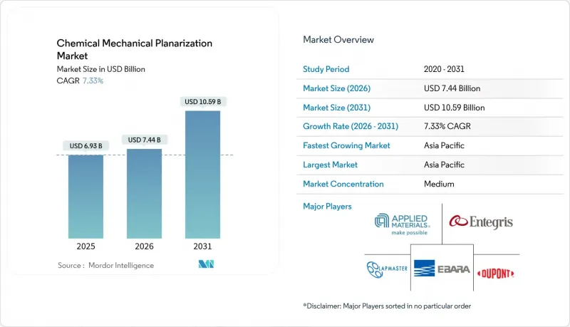
预计到 2026 年,化学机械抛光 (CMP) 市场规模将达到 74.4 亿美元,高于 2025 年的 69.3 亿美元。
预计到 2031 年将达到 105.9 亿美元,2026 年至 2031 年的复合年增长率为 7.33%。
成长的驱动力来自FinFET电晶体向环栅(GAA)电晶体的过渡、3D整合技术的发展,以及碳化硅(SiC)和氮化镓(GaN)在功率元件中日益广泛的应用。代工厂持续扩大大规模能,美国和欧盟的政府奖励也促进了本地化学机械抛光(CMP)供应链的发展。设备供应紧张限制了产能扩张,而永续性措施则加速了对低磨料和无磨料抛光液的需求。地缘政治出口限制正在重塑设备流通格局,并促进西方和中国供应商之间的平行创新交流。
全球化学机械抛光(CMP)市场趋势与洞察
加速采用GAA和3D积体电路
环栅(GAA)电晶体引入了新型金属栅堆迭结构,对化学机械抛光(CMP)製程提出了更高的选择性去除率和更严格的缺陷阈值要求,从而改变了CMP製程的本质。各大晶圆代工厂正计画量产3nm及以下GAA节点,这推动了配备先进终点控制功能的300mm单晶抛光机的设备更新换代。互补的3D整合技术,例如穿透硅通孔,需要在多个晶圆表面上实现超平整的铜层。因此,CMP平台整合了封闭回路型抛光垫调节和即时抛光液监控功能,以在更严格的公差范围内保持产量比率。
SiC/GaN功率元件的快速成长
碳化硅和氮化镓晶片具有高硬度和化学惰性,这显着增加了抛光时间和耗材成本。采用碱性化学成分和工程磨料的专用抛光液可达到接近 1µm/h 的去除率,同时将表面粗糙度保持在 0.05nm 以下。汽车电气化正在加速对这些材料的需求,促使工具製造商推出耐磨损且能防止碳化硅生产线与传统硅生产线交叉污染的抛光垫设计。
磨料投入成本飙升
当稀土元素供应紧张或化工厂进行检修时,氧化铈和过氧化氢等高纯度原料的价格会飙升。据美国地质调查局称,中国仍然是稀土元素进口的主要来源国,这使得全球浆料供应商容易受到贸易紧张局势的影响。供应商正在透过调整浆料配方、降低磨料含量以及透过过滤回收废液来应对这项挑战。
细分市场分析
到2025年,设备将占化学机械抛光(CMP)市场规模的62.78%。支出主要集中在单晶圆设备上,该设备可实现晶圆内亚奈米级不均匀性,并整合封闭回路型调谐功能以管理抛光垫表面状况。预计到2031年,该细分市场将以7.54%的复合年增长率成长,这主要得益于晶圆厂采用支援GAA製程和宽能带隙的新基板。同时,清洗模组也在升级,以去除7奈米以下製程节点的奈米级缺陷。
耗材占总收入的37.22%,其中以抛光液主导,其持续的需求确保了稳定的市场需求。二氧化硅基介电抛光液占据主导地位,而一些小众的氧化铈配方则用于玻璃和蓝宝石抛光。抛光垫供应商正在推出带有沟槽的聚合物混合物,以保持稳定的去除率,并在更长的使用寿命内最大限度地减少缺陷的产生。不断发展的永续性目标正在加速向低磨损性化学品的转变,使得当性能和环境指标相符时,耗材供应商能够获得更高的价格。
区域分析
预计到2025年,亚太地区将占全球营收的64.12%,并在2031年之前维持8.41%的复合年增长率。中国当地的本土化策略正推动晶圆厂建设的蓬勃发展,而台湾地区则继续保持主导。韩国正在加大对高层数3D NAND和DRAM的投资,从而推动了对介电层和金属平坦化产能的需求。日本供应商正利用其在超高纯度化学品和精密焊盘领域数十年的专业经验,进一步强化该地区垂直整合的生态系统。
北美地区营收排名第二。联邦政府的激励措施促进了新晶圆厂的建设,而由于客户优先考虑供应链安全,国内设备製造商也获得了大量订单。亚利桑那州和纽约州的先进封装计画刺激了符合在地采购规定的CMP耗材的区域需求。对中国高端抛光垫出口的限制正在分割市场,并提升北美CMP供应商的战略价值。
欧洲已设定目标,2030年实现全球半导体产量20%的目标,并将製造业的永续性放在首位。区域材料製造商正在扩大电子级过氧化氢和特殊浆料的产能,而德国和荷兰的设备製造商则正在调整其化学机械抛光(CMP)产品,使其符合欧盟的环境指令。政府资助的异质整合试点生产线正在推动研究中心和专业代工厂逐步引入CMP设备。
其他福利:
- Excel格式的市场预测(ME)表
- 3个月的分析师支持
目录
第一章 引言
- 研究假设和市场定义
- 调查范围
第二章调查方法
第三章执行摘要
第四章 市场情势
- 市场概览
- 市场驱动因素
- 加速采用GAA和3D积体电路
- SiC/GaN功率元件的快速成长
- 随着微型化进程的推进,节点特定的CMP步骤数量减少。
- 人工智慧资料中心资本投资的涟漪效应(高阶互连层)
- 美国和欧盟的晶圆厂激励措施推动了CMP供应的在地化。
- 向低磨蚀性浆料的永续性推进
- 市场限制
- 浆料投入成本(稀土元素)突然增加
- 300mm刀具的OEM生产能力紧张。
- 不同材料化学机械加工中的交叉污染风险
- 美国和中国对高端卫生棉和护髮素的出口限制
- 价值/供应链分析
- 监管环境
- 技术展望
- 波特五力分析
- 新进入者的威胁
- 供应商的议价能力
- 买方的议价能力
- 替代品的威胁
- 竞争对手之间的竞争
- 投资分析
第五章 市场规模与成长预测
- 依产品类型
- CMP设备
- 单晶圆CMP系统
- CMP后处理清洗设备
- 批量CMP系统
- 其他的
- CMP耗材
- CMP浆料
- 二氧化硅基浆料
- 氧化铝基浆料
- 氧化铈浆
- 复合材料/工程磨料浆料
- 其他材质(氧化锆、钻石等)
- 软垫
- 其他耗材(过滤器、CMP后处理用清洁剂等)
- CMP浆料
- CMP设备
- 透过使用
- 积体电路
- 化合物半导体
- 微机电系统(MEMS)和奈米机电系统(NEMS)
- 先进包装
- 其他用途
- 最终用户
- 铸造厂
- 整合装置製造商(IDM)
- 半导体外包组装和测试 (OSAT)
- 研发机构/大学
- 按地区
- 北美洲
- 我们
- 加拿大
- 墨西哥
- 欧洲
- 德国
- 法国
- 英国
- 义大利
- 其他欧洲地区
- 亚太地区
- 中国
- 日本
- 韩国
- 印度
- 亚太其他地区
- 南美洲
- 巴西
- 阿根廷
- 南美洲其他地区
- 中东
- 以色列
- 沙乌地阿拉伯
- 阿拉伯聯合大公国
- 其他中东地区
- 非洲
- 南非
- 埃及
- 其他非洲地区
- 北美洲
第六章 竞争情势
- 市场集中度分析
- 策略趋势与发展
- 供应商定位分析
- 公司简介
- Applied Materials Inc.
- Entegris Inc.
- EBARA Corporation
- Lapmaster Wolters GmbH
- DuPont de Nemours, Inc.
- Fujimi Incorporated
- Revasum Inc.
- Resonac Holdings Corporation
- Okamoto Corporation
- FUJIFILM Corporation
- Tokyo Seimitsu Co., Ltd.
- Lam Research Corporation
- KLA Corporation
- Hitachi High-Tech Corporation
- Cabot Microelectronics Corporation
- 3M Company
- Saint-Gobain Surface Conditioning
- BASF SE
- Nagase ChemteX Corporation
- Ace Nanochem Co., Ltd.
第七章 市场机会与未来展望
Chemical mechanical planarization market size in 2026 is estimated at USD 7.44 billion, growing from 2025 value of USD 6.93 billion with 2031 projections showing USD 10.59 billion, growing at 7.33% CAGR over 2026-2031.
Growth is propelled by the transition from FinFET to gate-all-around (GAA) transistors, 3D-integration, and the rising use of silicon carbide (SiC) and gallium nitride (GaN) in power devices. Foundries continue large-scale capacity additions, and government incentives in the United States and European Union encourage local CMP supply chains. Tight tool availability constrains production ramps, while sustainability initiatives accelerate demand for low-abrasive and abrasive-free slurries. Geopolitical export controls reshape equipment flows and spur parallel innovation tracks between Western and Chinese vendors.
Global Chemical Mechanical Planarization Market Trends and Insights
Accelerating GAA and 3D-IC adoption
Gate-all-around transistors alter CMP chemistries by introducing new metal gate stacks that require highly selective removal rates and tighter defectivity thresholds. Leading foundries have scheduled volume production of GAA nodes below 3 nm, driving an equipment refresh cycle for 300 mm single-wafer polishers with advanced endpoint control. Complementary 3D-integration techniques, such as through-silicon vias, demand ultra-flat copper layers across multiple wafer surfaces. CMP platforms, therefore, integrate closed-loop pad conditioning and real-time slurry monitoring to sustain yields at ever-smaller tolerances .
Rapid growth in SiC/GaN power devices
Silicon carbide and gallium nitride wafers exhibit hardness and chemical inertness that multiply polish times and consumable costs. Dedicated slurries using alkaline chemistries and engineered abrasives now achieve removal rates near 1 µm/h while holding surface roughness below 0.05 nm. Automotive electrification accelerates demand for these materials, prompting tool makers to release pad designs resilient to abrasive wear and cross-contamination shielding between SiC and traditional silicon lines.
Escalating slurry input costs
Cerium oxide, hydrogen peroxide, and other high-purity inputs show price spikes when rare-earth supply tightens or chemical plants undergo maintenance. The U.S. Geological Survey notes China remains the main source of rare-earth imports, leaving global slurry vendors exposed to trade disputes . Vendors respond by reformulating slurries with lower abrasive loads and recycling spent solutions through filtration loops.
Other drivers and restraints analyzed in the detailed report include:
- AI datacenter capital expenditure
- U.S. and EU fab incentives
- Tight OEM capacity for 300 mm tools
For complete list of drivers and restraints, kindly check the Table Of Contents.
Segment Analysis
Equipment represented 62.78% of the chemical mechanical planarization market size in 2025. Spending concentrates on single-wafer tools that deliver within-wafer non-uniformity below 1 nm and integrate closed-loop conditioning for pad surface health. The segment is forecast to rise at a 7.54% CAGR to 2031 as fabs install new platforms that support GAA processes and wide-bandgap substrates. Cleaning modules undergo concurrent upgrades to remove nanoscale defects at sub-7 nm nodes.
Consumables account for 37.22% of revenue, led by slurries whose recurring nature ensures stable demand. Silica-based dielectric slurries dominate, while niche ceria formulas address glass and sapphire polishing. Pad suppliers release grooved polymer blends that sustain consistent removal rates and minimize defectivity over extended pad life. Sustainability goals accelerate the shift to low-abrasive chemistries, positioning consumables vendors for premium pricing when performance and environmental metrics converge.
The Chemical Mechanical Planarization Market Report is Segmented by Product Type (CMP Equipment, CMP Consumables), Application (Integrated Circuit, Compound Semiconductor, MEMS and NEMS, Advanced Packaging, Other Applications), End-User (Foundries, Idms, OSAT, R&D Institutes/Universities), and Geography (North America, Europe, Asia Pacific, Rest of World). The Market Forecasts are Provided in Terms of Value (USD).
Geography Analysis
Asia Pacific generated 64.12% of 2025 revenue and is projected to record an 8.41% CAGR through 2031. Mainland China's localization push prompts aggressive wafer-fab construction, while Taiwan retains leadership in cutting-edge logic and advanced packaging. South Korea invests in high-layer count 3D NAND and DRAM, boosting demand for dielectric and metal planarization capacity. Japanese suppliers leverage decades-long expertise in ultrapure chemicals and precision pads, reinforcing the region's vertically integrated ecosystem.
North America ranks second by revenue. Federal incentives have unlocked new fab commitments, and domestic equipment leaders capture significant orders as customers prioritize secure supply chains. Advanced packaging initiatives in Arizona and New York stimulate regional demand for CMP consumables that comply with local content rules. Export controls limit high-end pad shipments to China, creating a bifurcated market and heightening strategic value for North American CMP vendors.
Europe pursues 20% global semiconductor output by 2030, emphasizing manufacturing sustainability. Regional materials firms expand electronics-grade hydrogen peroxide and specialty slurry capacity, while equipment makers in Germany and the Netherlands align CMP offerings with EU environmental directives. Government funding supports pilot lines for heterogeneous integration, driving incremental CMP tool installations across research hubs and specialty foundries.
- Applied Materials Inc.
- Entegris Inc.
- EBARA Corporation
- Lapmaster Wolters GmbH
- DuPont de Nemours, Inc.
- Fujimi Incorporated
- Revasum Inc.
- Resonac Holdings Corporation
- Okamoto Corporation
- FUJIFILM Corporation
- Tokyo Seimitsu Co., Ltd.
- Lam Research Corporation
- KLA Corporation
- Hitachi High-Tech Corporation
- Cabot Microelectronics Corporation
- 3M Company
- Saint-Gobain Surface Conditioning
- BASF SE
- Nagase ChemteX Corporation
- Ace Nanochem Co., Ltd.
Additional Benefits:
- The market estimate (ME) sheet in Excel format
- 3 months of analyst support
TABLE OF CONTENTS
1 INTRODUCTION
- 1.1 Study Assumptions and Market Definition
- 1.2 Scope of the Study
2 RESEARCH METHODOLOGY
3 EXECUTIVE SUMMARY
4 MARKET LANDSCAPE
- 4.1 Market Overview
- 4.2 Market Drivers
- 4.2.1 Accelerating GAA and 3D-IC adoption
- 4.2.2 Rapid growth in SiC/GaN power devices
- 4.2.3 Shrinking node-specific CMP step count
- 4.2.4 AI datacenter capex pull-through (advanced interconnect layers)
- 4.2.5 U.S. and EU fab incentives localizing CMP supply
- 4.2.6 Sustainability push for low-abrasive slurries
- 4.3 Market Restraints
- 4.3.1 Escalating slurry input costs (rare earths)
- 4.3.2 Tight OEM capacity for 300 mm tools
- 4.3.3 Cross-contamination risk in hetero-material CMP
- 4.3.4 China-US export controls on high-end pads and conditioners
- 4.4 Value / Supply-Chain Analysis
- 4.5 Regulatory Landscape
- 4.6 Technological Outlook
- 4.7 Porter Five Forces Analysis
- 4.7.1 Threat of New Entrants
- 4.7.2 Bargaining Power of Suppliers
- 4.7.3 Bargaining Power of Buyers
- 4.7.4 Threat of Substitutes
- 4.7.5 Competitive Rivalry
- 4.8 Investment Analysis
5 MARKET SIZE AND GROWTH FORECASTS (VALUE)
- 5.1 By Product Type
- 5.1.1 CMP Equipment
- 5.1.1.1 Single-Wafer CMP Systems
- 5.1.1.2 Post-CMP Cleaning Equipment
- 5.1.1.3 Batch CMP Systems
- 5.1.1.4 Others
- 5.1.2 CMP Consumables
- 5.1.2.1 CMP Slurry
- 5.1.2.1.1 Silica-Based Slurry
- 5.1.2.1.2 Aluminum Oxide-Based Slurry
- 5.1.2.1.3 Cerium Oxide-Based Slurry
- 5.1.2.1.4 Composite/Engineered Abrasive Slurry
- 5.1.2.1.5 Other (Zirconia, Diamond, etc.)
- 5.1.2.2 Pads
- 5.1.2.3 Other Consumables (Filters, Post-CMP Clean Chemistries, etc.)
- 5.1.2.1 CMP Slurry
- 5.1.1 CMP Equipment
- 5.2 By Application
- 5.2.1 Integrated Circuit
- 5.2.2 Compound Semiconductor
- 5.2.3 MEMS and NEMS
- 5.2.4 Advanced Packaging
- 5.2.5 Other Applications
- 5.3 By End-User
- 5.3.1 Foundries
- 5.3.2 Integrated Device Manufacturers (IDMs)
- 5.3.3 Outsourced Semiconductor Assembly and Test (OSAT)
- 5.3.4 R&D Institutes / Universities
- 5.4 By Geography
- 5.4.1 North America
- 5.4.1.1 United States
- 5.4.1.2 Canada
- 5.4.1.3 Mexico
- 5.4.2 Europe
- 5.4.2.1 Germany
- 5.4.2.2 France
- 5.4.2.3 United Kingdom
- 5.4.2.4 Italy
- 5.4.2.5 Rest of Europe
- 5.4.3 Asia Pacific
- 5.4.3.1 China
- 5.4.3.2 Japan
- 5.4.3.3 South Korea
- 5.4.3.4 India
- 5.4.3.5 Rest of Asia Pacific
- 5.4.4 South America
- 5.4.4.1 Brazil
- 5.4.4.2 Argentina
- 5.4.4.3 Rest of South America
- 5.4.5 Middle East
- 5.4.5.1 Israel
- 5.4.5.2 Saudi Arabia
- 5.4.5.3 United Arab Emirates
- 5.4.5.4 Rest of Middle East
- 5.4.6 Africa
- 5.4.6.1 South Africa
- 5.4.6.2 Egypt
- 5.4.6.3 Rest of Africa
- 5.4.1 North America
6 COMPETITIVE LANDSCAPE
- 6.1 Market Concentration Analysis
- 6.2 Strategic Moves and Developments
- 6.3 Vendor Positioning Analysis
- 6.4 Company Profiles (includes Global level Overview, Market level overview, Core Segments, Financials as available, Strategic Information, Products and Services, and Recent Developments)
- 6.4.1 Applied Materials Inc.
- 6.4.2 Entegris Inc.
- 6.4.3 EBARA Corporation
- 6.4.4 Lapmaster Wolters GmbH
- 6.4.5 DuPont de Nemours, Inc.
- 6.4.6 Fujimi Incorporated
- 6.4.7 Revasum Inc.
- 6.4.8 Resonac Holdings Corporation
- 6.4.9 Okamoto Corporation
- 6.4.10 FUJIFILM Corporation
- 6.4.11 Tokyo Seimitsu Co., Ltd.
- 6.4.12 Lam Research Corporation
- 6.4.13 KLA Corporation
- 6.4.14 Hitachi High-Tech Corporation
- 6.4.15 Cabot Microelectronics Corporation
- 6.4.16 3M Company
- 6.4.17 Saint-Gobain Surface Conditioning
- 6.4.18 BASF SE
- 6.4.19 Nagase ChemteX Corporation
- 6.4.20 Ace Nanochem Co., Ltd.
7 MARKET OPPORTUNITIES AND FUTURE OUTLOOK
- 7.1 White-space and Unmet-Need Assessment
 全球化学机械抛光(CMP)市场规模、份额、趋势和成长分析报告(2026-2034年)
 2026年全球化学机械抛光(CMP)浆料和抛光垫市场报告2026年全球化学机械抛光(CMP)市场报告化学机械抛光浆料市场-2026-2031年预测
 半导体用CMP材料市场:按类型、应用、通路和最终用户划分-2026年至2032年全球预测晶圆CMP材料市场按产品类型、晶圆尺寸、颗粒尺寸、应用和最终用途产业划分-2026-2032年全球预测
 湿式工作台市场:按类型、应用和地区划分
 机械式和电子式引信:全球市场份额和排名、总销售额和需求预测(2025-2031 年)化学机械平坦化市场按组件、晶圆尺寸和应用划分 - 全球预测 2025-2032
 全球半导体晶圆 CMP 固定环市场 - 市场份额和排名、总收入和需求预测(2025-2031 年)