


 |
市场调查报告书
商品编码
1355723
2023-2030 年全球半导体键结设备市场规模研究与预测(按类型、应用和区域分析)Global Semiconductor Bonding Equipment Market Size study & Forecast, by Type, by Application, and Regional Analysis, 2023-2030 |
||||||
全球半导体键合设备市场预计在 2023 年至 2030 年预测期内将以超过 11.76% 的健康成长率成长。晶圆基板键合单元用于在晶圆键合过程中将薄衬底晶圆黏附到支撑载体盘上。这是透过使用需要不同工具或设备的各种黏合程序来完成的。永久键结、瞬时键结和混合键结都是设备的形式。原子结合在一起,在半导体排列中产生同质结构,用于创建各种积体电路 (Ic) 和生产设备。在整个黏合模型中,材料的结构是一致的且几乎相同。市场成长是由关键因素推动的,例如各种应用对半导体晶片的需求不断增长以及半导体製造商增加投资以扩大其製造能力。
根据 Statista 的数据,2022 年全球半导体产业的销售额略低于 6,000 亿美元,比前一年的总收入 5,950 亿美元有所成长。预计到2024 年,半导体市场收入仅为6,309 亿美元。此外,2022 年12 月,中国宣布了一项价值超过1 兆元人民币(1,430 亿美元)的半导体产业补贴计划,这大大提高了晶片自给率和是对美国阻碍其技术进步的回应。预计大部分财政援助将用于资助中国企业收购国产半导体设备,这可能会提振地区市场需求。此外,近年来,汽车产业采用物联网和人工智慧以及提供下一代半导体键合解决方案的技术投资创造了利润丰厚的机会。然而,电路小型化导致的高拥有成本和复杂性的增加抑制了 2023-2030 年预测期内的市场成长。
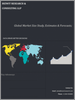
全球半导体键合设备市场研究考量的关键区域包括:亚太地区、北美、欧洲、拉丁美洲以及中东和非洲。亚太地区在全球市场份额中处于领先地位,由于支持半导体行业的投资不断增加以及国内主要供应商的战略投资,预计将成为增长最快的地区。
研究的目的是确定近年来不同细分市场和国家的市场规模,并预测未来几年的价值。该报告旨在纳入参与研究的国家内该行业的定性和定量方面。
该报告还提供了有关驱动因素和挑战等关键方面的详细信息,这些因素将决定市场的未来成长。此外,它还纳入了利害关係人投资的微观市场的潜在机会,以及对主要参与者的竞争格局和产品供应的详细分析。
目录
第 1 章:执行摘要
- 市场概况
- 2020-2030 年全球与细分市场估计与预测
- 2020-2030 年半导体键结设备市场(按地区)
- 2020-2030 年半导体键结设备市场(按类型)
- 2020-2030 年半导体键结设备市场(按应用)
- 主要趋势
- 估算方法
- 研究假设
第 2 章:全球半导体键结设备市场定义与范围
- 研究目的
- 市场定义和范围
- 产业演变
- 研究范围
- 研究考虑的年份
- 货币兑换率
第 3 章:全球半导体键结设备市场动态
- 半导体键合设备市场影响分析(2020-2030)
- 市场驱动因素
- 各种应用对半导体晶片的需求不断增长
- 半导体製造商增加投资以扩大製造能力
- 市场挑战
- 拥有成本高
- 电路小型化导致复杂度增加
- 市场机会
- 物联网和人工智慧在汽车领域的采用
- 提供下一代半导体键结解决方案的技术投资
- 市场驱动因素
第 4 章:全球半导体键结设备市场产业分析
- 波特的五力模型
- 供应商的议价能力
- 买家的议价能力
- 新进入者的威胁
- 替代品的威胁
- 竞争竞争
- 波特的五力影响分析
- PEST分析
- 政治的
- 经济
- 社会的
- 技术性
- 环境的
- 合法的
- 顶级投资机会
- 最佳制胜策略
- COVID-19 影响分析
- 颠覆性趋势
- 产业专家视角
- 分析师推荐与结论
第 5 章:全球半导体键结设备市场(按类型)
- 市场概况
- 全球半导体键结设备市场按类型、性能-潜力分析
- 2020-2030 年按类型分類的全球半导体键结设备市场估计与预测
- 半导体键合设备市场区隔分析
- 永久黏合设备
- 临时黏接设备
- 混合键合设备
第 6 章:全球半导体键结设备市场(按应用)
- 市场概况
- 全球半导体键结设备市场(按应用、性能)-潜力分析
- 2020-2030 年全球半导体键结设备市场估计及应用预测
- 半导体键合设备市场区隔分析
- 先进封装
- 电源IC和功率分立元件
- 光子装置
- MEMS 感测器和执行器
- 工程基材
- CMOS 影像感测器 (CIS)
第 7 章:全球半导体键结设备市场,区域分析
- 领先国家
- 顶尖新兴国家
- 半导体键结设备市场,区域市场概况
- 北美洲
- 我们
- 2020-2030 年型别细分估计与预测
- 2020-2030 年应用细分估计与预测
- 加拿大
- 我们
- 欧洲半导体键结设备市场概况
- 英国
- 德国
- 法国
- 西班牙
- 义大利
- 欧洲其他地区
- 亚太地区半导体键结设备市场概况
- 中国
- 印度
- 日本
- 澳洲
- 韩国
- 亚太地区其他地区
- 拉丁美洲半导体键结设备市场概况
- 巴西
- 墨西哥
- 中东和非洲
- 沙乌地阿拉伯
- 南非
- 中东和非洲其他地区
第 8 章:竞争情报
- 重点企业SWOT分析
- 公司1
- 公司2
- 公司3
- 顶级市场策略
- 公司简介
- Kulicke and Soffa Industries Inc.
- 关键讯息
- 概述
- 财务(视数据可用性而定)
- 产品概要
- 最近的发展
- EV Group
- ASMPT Semiconductor Solutions
- MRSI Systems. (Myronic AB)
- WestBond Inc.
- Panasonic Industry Co. Ltd.
- Palomar Technologies
- Dr. Tresky AG
- BE Semiconductor Industries NV
- Fasford Technology Co.Ltd (Fuji Group)
第 9 章:研究过程
- 研究过程
- 资料探勘
- 分析
- 市场预测
- 验证
- 出版
- 研究属性
- 研究假设
Global Semiconductor Bonding Equipment Markeis anticipated to grow with a healthy growth rate of more than 11.76% over the forecast period 2023-2030. Wafer substrate bonding units are used to adhere a thin substrate wafer to a support carrier disc during the wafer bonding process. This is accomplished using a variety of bonding procedures that call for different tools or equipment. Permanent bonding, transient bonding, and hybrid bonding are all forms of equipment. Atoms are bound together to produce a homogenous structure in semiconductor arrangements, which are utilized to create various integrated circuits (Ics) and production equipment. The material's structure is consistent and almost identical throughout the bonding model. The market growth is driven by key factors such as rising demand for Semiconductor Chips across various applications and increasing investment by Semiconductor manufacturers to expand their manufacturing capacity.
According to Statista, the worldwide semiconductor industry generated slightly under 600 billion dollars in sales in 2022, an increase from the previous year when total revenues totaled 595 billion dollars. The semiconductor market's revenues are only projected to be 630.9 billion dollars in 2024. Additionally, in December 2022, China announced a subsidy program for its semiconductor sector worth more than CNY 1 trillion (USD 143 billion), which considerably increased chip self-sufficiency and was a response to American efforts to hinder its technological advancement. The majority of the financial aid is expected to be utilized to finance Chinese companies' acquisitions of domestic semiconductor equipment, which will likely boost regional market demand. Moreover, adoption of IoT and AI in the automotive sector and technological investments in offering next-generation semiconductor bonding solutions create lucrative opportunities during the years. However, high cost of ownership and increased complexity owing to miniaturization of circuits stifle market growth throughout the forecast period of 2023-2030.
The key regions considered for the Global Semiconductor Bonding Equipment Market study include: Asia Pacific, North America, Europe, Latin America, and Middle East & Africa. Asia Pacific is leading the global market share and expected to be the fastest growing region owing to growing investments to support the semiconductor industry and strategic investments by key domestic suppliers.
Major market players included in this report are:
- Kulicke and Soffa Industries Inc.
- EV Group
- ASMPT Semiconductor Solutions
- MRSI Systems. (Myronic AB)
- WestBond Inc.
- Panasonic Industry Co. Ltd.
- Palomar Technologies
- Dr. Tresky AG
- BE Semiconductor Industries NV
- Fasford Technology Co.Ltd (Fuji Group)
Recent Developments in the Market:
- October 2022, a new semiconductor assembly and testing facility is likely to be built in Penang, according to proposals released by BE Semiconductor Industries NV. The new facility, which consists of two buildings (Plants 4 and 5), will be in the Bayan Lepas Free Industrial Zone and have a total built-up area of 982,000 square feet. The project is anticipated to be finished in 2025 and would open over 2,700 job possibilities in the location.
- July 2022, the most recent development in the MRSI-H/HVM-series product line, MRSI-H-HPLD+, has been introduced by MRSI Systems (Mycronic Group). In order to dramatically increase productivity utilising parallel processing while preserving excellent precision and flexibility, this new variation of MRSI-H-HPLD is designed for high-power laser die attachment applications.
Global Semiconductor Bonding Equipment Market Report Scope:
- Historical Data: 2020 - 2021
- Base Year for Estimation: 2022
- Forecast period: 2023-2030
- Report Coverage: Revenue forecast, Company Ranking, Competitive Landscape, Growth factors, and Trends
- Segments Covered: Type, Application, Region
- Regional Scope: North America; Europe; Asia Pacific; Latin America; Middle East & Africa
- Customization Scope: Free report customization (equivalent up to 8 analyst's working hours) with purchase. Addition or alteration to country, regional & segment scope*
The objective of the study is to define market sizes of different segments & countries in recent years and to forecast the values to the coming years. The report is designed to incorporate both qualitative and quantitative aspects of the industry within countries involved in the study.
The report also caters detailed information about the crucial aspects such as driving factors & challenges which will define the future growth of the market. Additionally, it also incorporates potential opportunities in micro markets for stakeholders to invest along with the detailed analysis of competitive landscape and product offerings of key players. The detailed segments and sub-segment of the market are explained below:
By Type:
- Permanent Bonding Equipment
- Temporary Bonding Equipment
- Hybrid Bonding Equipment
By Application:
- Advanced Packaging
- Power IC and Power Discrete
- Photonic Devices
- MEMS Sensors and Actuators
- Engineered Substrates
- CMOS Image Sensors (CIS)
By Region:
- North America
- U.S.
- Canada
- Europe
- UK
- Germany
- France
- Spain
- Italy
- ROE
- Asia Pacific
- China
- India
- Japan
- Australia
- South Korea
- RoAPAC
- Latin America
- Brazil
- Mexico
- Middle East & Africa
- Saudi Arabia
- South Africa
- Rest of Middle East & Africa
Table of Contents
Chapter 1. Executive Summary
- 1.1. Market Snapshot
- 1.2. Global & Segmental Market Estimates & Forecasts, 2020-2030 (USD Billion)
- 1.2.1. Semiconductor Bonding Equipment Market, by Region, 2020-2030 (USD Billion)
- 1.2.2. Semiconductor Bonding Equipment Market, by Type, 2020-2030 (USD Billion)
- 1.2.3. Semiconductor Bonding Equipment Market, by Application, 2020-2030 (USD Billion)
- 1.3. Key Trends
- 1.4. Estimation Methodology
- 1.5. Research Assumption
Chapter 2. Global Semiconductor Bonding Equipment Market Definition and Scope
- 2.1. Objective of the Study
- 2.2. Market Definition & Scope
- 2.2.1. Industry Evolution
- 2.2.2. Scope of the Study
- 2.3. Years Considered for the Study
- 2.4. Currency Conversion Rates
Chapter 3. Global Semiconductor Bonding Equipment Market Dynamics
- 3.1. Semiconductor Bonding Equipment Market Impact Analysis (2020-2030)
- 3.1.1. Market Drivers
- 3.1.1.1. Rising Demand for Semiconductor Chips across Various Applications
- 3.1.1.2. Increasing Investment by Semiconductor Manufacturers to Expand their Manufacturing Capacity
- 3.1.2. Market Challenges
- 3.1.2.1. High Cost of Ownership
- 3.1.2.2. Increased Complexity Owing to Miniaturization of Circuits
- 3.1.3. Market Opportunities
- 3.1.3.1. Adoption of IoT and AI in the automotive sector
- 3.1.3.2. Technological investments in offering next-generation semiconductor bonding solutions
- 3.1.1. Market Drivers
Chapter 4. Global Semiconductor Bonding Equipment Market Industry Analysis
- 4.1. Porter's 5 Force Model
- 4.1.1. Bargaining Power of Suppliers
- 4.1.2. Bargaining Power of Buyers
- 4.1.3. Threat of New Entrants
- 4.1.4. Threat of Substitutes
- 4.1.5. Competitive Rivalry
- 4.2. Porter's 5 Force Impact Analysis
- 4.3. PEST Analysis
- 4.3.1. Political
- 4.3.2. Economical
- 4.3.3. Social
- 4.3.4. Technological
- 4.3.5. Environmental
- 4.3.6. Legal
- 4.4. Top investment opportunity
- 4.5. Top winning strategies
- 4.6. COVID-19 Impact Analysis
- 4.7. Disruptive Trends
- 4.8. Industry Expert Perspective
- 4.9. Analyst Recommendation & Conclusion
Chapter 5. Global Semiconductor Bonding Equipment Market, by Type
- 5.1. Market Snapshot
- 5.2. Global Semiconductor Bonding Equipment Market by Type, Performance - Potential Analysis
- 5.3. Global Semiconductor Bonding Equipment Market Estimates & Forecasts by Type 2020-2030 (USD Billion)
- 5.4. Semiconductor Bonding Equipment Market, Sub Segment Analysis
- 5.4.1. Permanent Bonding Equipment
- 5.4.2. Temporary Bonding Equipment
- 5.4.3. Hybrid Bonding Equipment
Chapter 6. Global Semiconductor Bonding Equipment Market, by Application
- 6.1. Market Snapshot
- 6.2. Global Semiconductor Bonding Equipment Market by Application, Performance - Potential Analysis
- 6.3. Global Semiconductor Bonding Equipment Market Estimates & Forecasts by Application 2020-2030 (USD Billion)
- 6.4. Semiconductor Bonding Equipment Market, Sub Segment Analysis
- 6.4.1. Advanced Packaging
- 6.4.2. Power IC and Power Discrete
- 6.4.3. Photonic Devices
- 6.4.4. MEMS Sensors and Actuators
- 6.4.5. Engineered Substrates
- 6.4.6. CMOS Image Sensors (CIS)
Chapter 7. Global Semiconductor Bonding Equipment Market, Regional Analysis
- 7.1. Top Leading Countries
- 7.2. Top Emerging Countries
- 7.3. Semiconductor Bonding Equipment Market, Regional Market Snapshot
- 7.4. North America Semiconductor Bonding Equipment Market
- 7.4.1. U.S. Semiconductor Bonding Equipment Market
- 7.4.1.1. Type breakdown estimates & forecasts, 2020-2030
- 7.4.1.2. Application breakdown estimates & forecasts, 2020-2030
- 7.4.2. Canada Semiconductor Bonding Equipment Market
- 7.4.1. U.S. Semiconductor Bonding Equipment Market
- 7.5. Europe Semiconductor Bonding Equipment Market Snapshot
- 7.5.1. U.K. Semiconductor Bonding Equipment Market
- 7.5.2. Germany Semiconductor Bonding Equipment Market
- 7.5.3. France Semiconductor Bonding Equipment Market
- 7.5.4. Spain Semiconductor Bonding Equipment Market
- 7.5.5. Italy Semiconductor Bonding Equipment Market
- 7.5.6. Rest of Europe Semiconductor Bonding Equipment Market
- 7.6. Asia-Pacific Semiconductor Bonding Equipment Market Snapshot
- 7.6.1. China Semiconductor Bonding Equipment Market
- 7.6.2. India Semiconductor Bonding Equipment Market
- 7.6.3. Japan Semiconductor Bonding Equipment Market
- 7.6.4. Australia Semiconductor Bonding Equipment Market
- 7.6.5. South Korea Semiconductor Bonding Equipment Market
- 7.6.6. Rest of Asia Pacific Semiconductor Bonding Equipment Market
- 7.7. Latin America Semiconductor Bonding Equipment Market Snapshot
- 7.7.1. Brazil Semiconductor Bonding Equipment Market
- 7.7.2. Mexico Semiconductor Bonding Equipment Market
- 7.8. Middle East & Africa Semiconductor Bonding Equipment Market
- 7.8.1. Saudi Arabia Semiconductor Bonding Equipment Market
- 7.8.2. South Africa Semiconductor Bonding Equipment Market
- 7.8.3. Rest of Middle East & Africa Semiconductor Bonding Equipment Market
Chapter 8. Competitive Intelligence
- 8.1. Key Company SWOT Analysis
- 8.1.1. Company 1
- 8.1.2. Company 2
- 8.1.3. Company 3
- 8.2. Top Market Strategies
- 8.3. Company Profiles
- 8.3.1. Kulicke and Soffa Industries Inc.
- 8.3.1.1. Key Information
- 8.3.1.2. Overview
- 8.3.1.3. Financial (Subject to Data Availability)
- 8.3.1.4. Product Summary
- 8.3.1.5. Recent Developments
- 8.3.2. EV Group
- 8.3.3. ASMPT Semiconductor Solutions
- 8.3.4. MRSI Systems. (Myronic AB)
- 8.3.5. WestBond Inc.
- 8.3.6. Panasonic Industry Co. Ltd.
- 8.3.7. Palomar Technologies
- 8.3.8. Dr. Tresky AG
- 8.3.9. BE Semiconductor Industries NV
- 8.3.10. Fasford Technology Co.Ltd (Fuji Group)
- 8.3.1. Kulicke and Soffa Industries Inc.
Chapter 9. Research Process
- 9.1. Research Process
- 9.1.1. Data Mining
- 9.1.2. Analysis
- 9.1.3. Market Estimation
- 9.1.4. Validation
- 9.1.5. Publishing
- 9.2. Research Attributes
- 9.3. Research Assumption
LIST OF TABLES
- TABLE 1. Global Semiconductor Bonding Equipment Market, report scope
- TABLE 2. Global Semiconductor Bonding Equipment Market estimates & forecasts by Region 2020-2030 (USD Billion)
- TABLE 3. Global Semiconductor Bonding Equipment Market estimates & forecasts by Type 2020-2030 (USD Billion)
- TABLE 4. Global Semiconductor Bonding Equipment Market estimates & forecasts by Application 2020-2030 (USD Billion)
- TABLE 5. Global Semiconductor Bonding Equipment Market by segment, estimates & forecasts, 2020-2030 (USD Billion)
- TABLE 6. Global Semiconductor Bonding Equipment Market by region, estimates & forecasts, 2020-2030 (USD Billion)
- TABLE 7. Global Semiconductor Bonding Equipment Market by segment, estimates & forecasts, 2020-2030 (USD Billion)
- TABLE 8. Global Semiconductor Bonding Equipment Market by region, estimates & forecasts, 2020-2030 (USD Billion)
- TABLE 9. Global Semiconductor Bonding Equipment Market by segment, estimates & forecasts, 2020-2030 (USD Billion)
- TABLE 10. Global Semiconductor Bonding Equipment Market by region, estimates & forecasts, 2020-2030 (USD Billion)
- TABLE 11. Global Semiconductor Bonding Equipment Market by segment, estimates & forecasts, 2020-2030 (USD Billion)
- TABLE 12. Global Semiconductor Bonding Equipment Market by region, estimates & forecasts, 2020-2030 (USD Billion)
- TABLE 13. Global Semiconductor Bonding Equipment Market by segment, estimates & forecasts, 2020-2030 (USD Billion)
- TABLE 14. Global Semiconductor Bonding Equipment Market by region, estimates & forecasts, 2020-2030 (USD Billion)
- TABLE 15. U.S. Semiconductor Bonding Equipment Market estimates & forecasts, 2020-2030 (USD Billion)
- TABLE 16. U.S. Semiconductor Bonding Equipment Market estimates & forecasts by segment 2020-2030 (USD Billion)
- TABLE 17. U.S. Semiconductor Bonding Equipment Market estimates & forecasts by segment 2020-2030 (USD Billion)
- TABLE 18. Canada Semiconductor Bonding Equipment Market estimates & forecasts, 2020-2030 (USD Billion)
- TABLE 19. Canada Semiconductor Bonding Equipment Market estimates & forecasts by segment 2020-2030 (USD Billion)
- TABLE 20. Canada Semiconductor Bonding Equipment Market estimates & forecasts by segment 2020-2030 (USD Billion)
- TABLE 21. UK Semiconductor Bonding Equipment Market estimates & forecasts, 2020-2030 (USD Billion)
- TABLE 22. UK Semiconductor Bonding Equipment Market estimates & forecasts by segment 2020-2030 (USD Billion)
- TABLE 23. UK Semiconductor Bonding Equipment Market estimates & forecasts by segment 2020-2030 (USD Billion)
- TABLE 24. Germany Semiconductor Bonding Equipment Market estimates & forecasts, 2020-2030 (USD Billion)
- TABLE 25. Germany Semiconductor Bonding Equipment Market estimates & forecasts by segment 2020-2030 (USD Billion)
- TABLE 26. Germany Semiconductor Bonding Equipment Market estimates & forecasts by segment 2020-2030 (USD Billion)
- TABLE 27. France Semiconductor Bonding Equipment Market estimates & forecasts, 2020-2030 (USD Billion)
- TABLE 28. France Semiconductor Bonding Equipment Market estimates & forecasts by segment 2020-2030 (USD Billion)
- TABLE 29. France Semiconductor Bonding Equipment Market estimates & forecasts by segment 2020-2030 (USD Billion)
- TABLE 30. Italy Semiconductor Bonding Equipment Market estimates & forecasts, 2020-2030 (USD Billion)
- TABLE 31. Italy Semiconductor Bonding Equipment Market estimates & forecasts by segment 2020-2030 (USD Billion)
- TABLE 32. Italy Semiconductor Bonding Equipment Market estimates & forecasts by segment 2020-2030 (USD Billion)
- TABLE 33. Spain Semiconductor Bonding Equipment Market estimates & forecasts, 2020-2030 (USD Billion)
- TABLE 34. Spain Semiconductor Bonding Equipment Market estimates & forecasts by segment 2020-2030 (USD Billion)
- TABLE 35. Spain Semiconductor Bonding Equipment Market estimates & forecasts by segment 2020-2030 (USD Billion)
- TABLE 36. RoE Semiconductor Bonding Equipment Market estimates & forecasts, 2020-2030 (USD Billion)
- TABLE 37. RoE Semiconductor Bonding Equipment Market estimates & forecasts by segment 2020-2030 (USD Billion)
- TABLE 38. RoE Semiconductor Bonding Equipment Market estimates & forecasts by segment 2020-2030 (USD Billion)
- TABLE 39. China Semiconductor Bonding Equipment Market estimates & forecasts, 2020-2030 (USD Billion)
- TABLE 40. China Semiconductor Bonding Equipment Market estimates & forecasts by segment 2020-2030 (USD Billion)
- TABLE 41. China Semiconductor Bonding Equipment Market estimates & forecasts by segment 2020-2030 (USD Billion)
- TABLE 42. India Semiconductor Bonding Equipment Market estimates & forecasts, 2020-2030 (USD Billion)
- TABLE 43. India Semiconductor Bonding Equipment Market estimates & forecasts by segment 2020-2030 (USD Billion)
- TABLE 44. India Semiconductor Bonding Equipment Market estimates & forecasts by segment 2020-2030 (USD Billion)
- TABLE 45. Japan Semiconductor Bonding Equipment Market estimates & forecasts, 2020-2030 (USD Billion)
- TABLE 46. Japan Semiconductor Bonding Equipment Market estimates & forecasts by segment 2020-2030 (USD Billion)
- TABLE 47. Japan Semiconductor Bonding Equipment Market estimates & forecasts by segment 2020-2030 (USD Billion)
- TABLE 48. South Korea Semiconductor Bonding Equipment Market estimates & forecasts, 2020-2030 (USD Billion)
- TABLE 49. South Korea Semiconductor Bonding Equipment Market estimates & forecasts by segment 2020-2030 (USD Billion)
- TABLE 50. South Korea Semiconductor Bonding Equipment Market estimates & forecasts by segment 2020-2030 (USD Billion)
- TABLE 51. Australia Semiconductor Bonding Equipment Market estimates & forecasts, 2020-2030 (USD Billion)
- TABLE 52. Australia Semiconductor Bonding Equipment Market estimates & forecasts by segment 2020-2030 (USD Billion)
- TABLE 53. Australia Semiconductor Bonding Equipment Market estimates & forecasts by segment 2020-2030 (USD Billion)
- TABLE 54. RoAPAC Semiconductor Bonding Equipment Market estimates & forecasts, 2020-2030 (USD Billion)
- TABLE 55. RoAPAC Semiconductor Bonding Equipment Market estimates & forecasts by segment 2020-2030 (USD Billion)
- TABLE 56. RoAPAC Semiconductor Bonding Equipment Market estimates & forecasts by segment 2020-2030 (USD Billion)
- TABLE 57. Brazil Semiconductor Bonding Equipment Market estimates & forecasts, 2020-2030 (USD Billion)
- TABLE 58. Brazil Semiconductor Bonding Equipment Market estimates & forecasts by segment 2020-2030 (USD Billion)
- TABLE 59. Brazil Semiconductor Bonding Equipment Market estimates & forecasts by segment 2020-2030 (USD Billion)
- TABLE 60. Mexico Semiconductor Bonding Equipment Market estimates & forecasts, 2020-2030 (USD Billion)
- TABLE 61. Mexico Semiconductor Bonding Equipment Market estimates & forecasts by segment 2020-2030 (USD Billion)
- TABLE 62. Mexico Semiconductor Bonding Equipment Market estimates & forecasts by segment 2020-2030 (USD Billion)
- TABLE 63. RoLA Semiconductor Bonding Equipment Market estimates & forecasts, 2020-2030 (USD Billion)
- TABLE 64. RoLA Semiconductor Bonding Equipment Market estimates & forecasts by segment 2020-2030 (USD Billion)
- TABLE 65. RoLA Semiconductor Bonding Equipment Market estimates & forecasts by segment 2020-2030 (USD Billion)
- TABLE 66. Saudi Arabia Semiconductor Bonding Equipment Market estimates & forecasts, 2020-2030 (USD Billion)
- TABLE 67. South Africa Semiconductor Bonding Equipment Market estimates & forecasts by segment 2020-2030 (USD Billion)
- TABLE 68. RoMEA Semiconductor Bonding Equipment Market estimates & forecasts by segment 2020-2030 (USD Billion)
- TABLE 69. List of secondary sources, used in the study of global Semiconductor Bonding Equipment Market
- TABLE 70. List of primary sources, used in the study of global Semiconductor Bonding Equipment Market
- TABLE 71. Years considered for the study
- TABLE 72. Exchange rates considered
List of tables and figures and dummy in nature, final lists may vary in the final deliverable
LIST OF FIGURES
- FIG 1. Global Semiconductor Bonding Equipment Market, research methodology
- FIG 2. Global Semiconductor Bonding Equipment Market, Market estimation techniques
- FIG 3. Global Market size estimates & forecast methods
- FIG 4. Global Semiconductor Bonding Equipment Market, key trends 2022
- FIG 5. Global Semiconductor Bonding Equipment Market, growth prospects 2023-2030
- FIG 6. Global Semiconductor Bonding Equipment Market, porters 5 force model
- FIG 7. Global Semiconductor Bonding Equipment Market, pest analysis
- FIG 8. Global Semiconductor Bonding Equipment Market, value chain analysis
- FIG 9. Global Semiconductor Bonding Equipment Market by segment, 2020 & 2030 (USD Billion)
- FIG 10. Global Semiconductor Bonding Equipment Market by segment, 2020 & 2030 (USD Billion)
- FIG 11. Global Semiconductor Bonding Equipment Market by segment, 2020 & 2030 (USD Billion)
- FIG 12. Global Semiconductor Bonding Equipment Market by segment, 2020 & 2030 (USD Billion)
- FIG 13. Global Semiconductor Bonding Equipment Market by segment, 2020 & 2030 (USD Billion)
- FIG 14. Global Semiconductor Bonding Equipment Market, regional snapshot 2020 & 2030
- FIG 15. North America Semiconductor Bonding Equipment Market 2020 & 2030 (USD Billion)
- FIG 16. Europe Semiconductor Bonding Equipment Market 2020 & 2030 (USD Billion)
- FIG 17. Asia Pacific Semiconductor Bonding Equipment Market 2020 & 2030 (USD Billion)
- FIG 18. Latin America Semiconductor Bonding Equipment Market 2020 & 2030 (USD Billion)
- FIG 19. Middle East & Africa Semiconductor Bonding Equipment Market 2020 & 2030 (USD Billion)
List of tables and figures and dummy in nature, final lists may vary in the final deliverable
 2023-2030 年全球半导体键结市场规模研究与预测(按类型、製程类型、键结技术、应用和区域分析)
 半导体键合设备 - 市场占有率分析、产业趋势与统计、成长预测(2024 - 2029)
 半导体键合设备市场报告:2030 年趋势、预测与竞争分析
 晶片邦定机设备市场报告:2030 年趋势、预测与竞争分析
 晶粒邦定机市场报告:2030 年趋势、预测与竞争分析
 半导体键结市场:按类型、应用分类 - 2024-2030 年全球预测
 半导体键结市场 - 2018-2028 年全球产业规模、份额、趋势、机会与预测,按类型、製程类型、键结技术、按应用、按竞争进行细分。
 半导体键结全球市场规模、份额、产业趋势分析报告:用途、类型、键结技术、製程类型、区域展望与预测,2023-2030
 焊线机设备的全球市场
 贴片机设备的全球市场