


 |
市场调查报告书
商品编码
1766204
砷化镓(GaAs)晶圆市场机会、成长动力、产业趋势分析及2025-2034年预测Gallium Arsenide (GaAs) Wafer Market Opportunity, Growth Drivers, Industry Trend Analysis, and Forecast 2025 - 2034 |
||||||
2024年,全球砷化镓晶圆市场规模达11.4亿美元,预计2034年将以11.8%的复合年增长率成长,达到35.1亿美元。这一成长主要归功于5G技术的广泛应用以及光子学和光电器件的进步。砷化镓凭藉其更高的电子迁移率和饱和速度,相较于硅等传统材料更具优势,适用于高频和高速应用。随着全球5G基础设施的加速部署,对采用砷化镓晶圆製造的射频元件的需求急剧成长。
这些晶圆对于开发支援更快资料传输速率和更低延迟的新一代无线系统组件至关重要。除电信领域外,GaAs晶圆因其直接带隙特性,在光电应用中也被广泛应用,从而支援高效的光发射和检测。通讯网路的不断发展,以及雷射技术和光电探测器应用的不断拓展,显着增强了主要经济体GaAs晶圆市场的成长动能。对高性能电子产品和安全供应链的日益关注,也支持了这些晶圆在策略领域的应用。
| 市场范围 | |
|---|---|
| 起始年份 | 2024 |
| 预测年份 | 2025-2034 |
| 起始值 | 11.4亿美元 |
| 预测值 | 35.1亿美元 |
| 复合年增长率 | 11.8% |
亚太地区正在成为砷化镓晶圆的生产中心,多个国家正在大力投资下一代电信基础设施,推动了对射频元件的需求。受5G快速普及和对先进无线系统日益增长的需求的推动,北美也正经历着强劲的发展势头。该地区日益依赖砷化镓晶圆来增强高频性能,凸显了其在现代通讯中的战略重要性。这种材料能够有效地以最小的延迟处理大资料流,这使得它对下一代技术至关重要。同时,全球光电产业正利用砷化镓优异的电子迁移率和带隙结构,继续将其整合到LED、雷射发射器和光感测器等装置中。
半绝缘GaAs晶圆(2024年价值6.8亿美元)引领此细分市场,因为它们是建造射频和微波元件的关键。其低载流子浓度和高电阻率使其成为製造射频开关和放大器的理想选择,这些装置广泛应用于各种高频通讯平台。半绝缘GaAs晶圆能够最大限度地降低讯号干扰,使其成为对精度和性能要求极高的环境中的首选。
预计到2034年,4吋GaAs晶圆市场规模将达到4.1亿美元。这类晶圆仍是製造业的首选,这主要归功于其与生产设备的良好相容性,以及在射频和光电元件领域的高使用量。它们在市场上的长期存在确保了稳定的供应链,并易于整合到商业规模营运中,使其成为许多应用的标准。
受国防、航太和无线通讯领域日益增长的需求推动,美国砷化镓 (GaAs) 晶圆市场规模预计在 2034 年达到 9.3 亿美元。随着美国优先考虑半导体的自主性和技术领先地位,公共和私人部门对增强 GaAs 基技术的投资正在加速。雷射雷达和卫星通讯等应用的日益普及,进一步推动了对 GaAs 晶圆的需求。扶持政策和专案研究正在推动创新,并提升该地区的国内生产能力。
积极影响砷化镓 (GaAs) 晶圆市场的关键参与者包括 WIN Semiconductors Corp.、IQE plc、住友电工株式会社、VPEC Inc.(Visual Photonics Epitaxy Company)和东芝公司。 GaAs 晶圆市场的知名参与者正在部署各种策略方针,以保持竞争优势并扩大其全球影响力。他们不断投资研发,以提高晶圆品质、提高生产效率并增强设备性能。与终端使用产业的策略合作正在帮助公司更好地使其产品与不断变化的应用需求保持一致。许多製造商也专注于扩大产能并建立区域製造中心,以满足当地需求,同时最大限度地降低供应链风险。此外,各公司正在加强其智慧财产权组合併推进专有外延技术,以确保产品差异化。
目录
第一章:方法论与范围
第二章:执行摘要
第三章:行业洞察
- 产业生态系统分析
- 川普政府关税
- 对贸易的影响
- 贸易量中断
- 报復措施
- 对产业的影响
- 供给侧影响(原料)
- 主要材料价格波动
- 供应链重组
- 生产成本影响
- 需求面影响(售价)
- 价格传导至终端市场
- 市占率动态
- 消费者反应模式
- 供给侧影响(原料)
- 受影响的主要公司
- 策略产业反应
- 供应链重组
- 定价和产品策略
- 政策参与
- 展望与未来考虑
- 对贸易的影响
- 供应商矩阵
- 利润率分析
- 技术与创新格局
- 专利分析
- 重要新闻和倡议
- 产业衝击力
- 成长动力
- 高频射频设备需求不断成长
- 光电子应用的扩展
- ADAS 和自动驾驶汽车的成长
- 太空和军事通讯领域的应用
- 向更大晶圆尺寸(6吋)过渡
- 产业陷阱与挑战
- 製造成本高且製造复杂
- 硅和 SiGe 技术进步
- 成长动力
- 成长潜力分析
- 监管格局
- 技术格局
- 未来市场趋势
- 差距分析
- 波特的分析
- PESTEL分析
第四章:竞争格局
- 介绍
- 公司市占率分析
- 主要市场参与者的竞争分析
- 竞争定位矩阵
- 策略仪表板
第五章:市场预估与预测:依晶圆类型,2021 - 2034
- 半绝缘GaAs芯片
- 半导体GaAs芯片
第六章:市场估计与预测:依晶圆尺寸,2021 - 2034
- 2英吋
- 4吋
- 6吋
- 8吋
第七章:市场估计与预测:按应用,2021 - 2034 年
- 射频 (RF) 设备
- 光电器件
- 光电设备
- 单晶片微波积体电路(MMIC)
第八章:市场估计与预测:依最终用途,2021 - 2034 年
- 电信
- 消费性电子产品
- 汽车
- 航太与国防
- 工业自动化
- 能源与电力
- 其他的
第九章:市场估计与预测:按地区,2021 - 2034 年
- 主要趋势
- 北美洲
- 我们
- 加拿大
- 欧洲
- 德国
- 英国
- 法国
- 西班牙
- 义大利
- 荷兰
- 亚太地区
- 中国
- 印度
- 日本
- 澳洲
- 韩国
- 拉丁美洲
- 巴西
- 墨西哥
- 阿根廷
- 中东和非洲
- 沙乌地阿拉伯
- 南非
- 阿联酋
第十章:公司简介
- Analog Devices Inc.
- AWSC (Advanced Wireless Semiconductor Company)
- AXT Inc.
- Broadcom Inc.
- Coherent Corp.
- Cree (Wolfspeed)
- Freiberger Compound Materials GmbH
- Fujitsu Semiconductor Limited
- IntelliEPI Inc.
- IQE plc
- MACOM Technology Solutions
- Northrop Grumman Corporation
- Qorvo Inc.
- RFHIC Corporation
- Skyworks Solutions Inc.
- Sumitomo Electric Industries, Ltd.
- Toshiba Corporation
- VPEC Inc.
- WIN Semiconductors Corp.
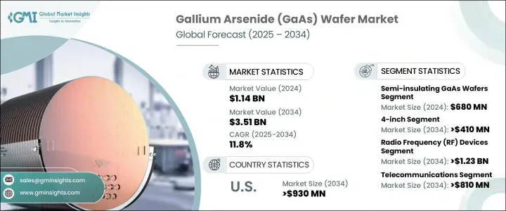
The Global Gallium Arsenide Wafer Market was valued at USD 1.14 billion in 2024 and is estimated to grow at a CAGR of 11.8% to reach USD 3.51 billion by 2034. The growth is largely attributed to the widespread adoption of 5G technology and advancements in photonics and optoelectronic devices. Gallium arsenide offers advantages over traditional materials like silicon due to its higher electron mobility and saturation velocity, making it suitable for high-frequency and high-speed applications. As the rollout of 5G infrastructure accelerates globally, the demand for RF components built using GaAs wafers has risen sharply.
These wafers are essential for developing components that power next-gen wireless systems by supporting faster data transfer rates and lower latency. Apart from telecommunications, GaAs wafers are heavily utilized in optoelectronic applications due to their direct bandgap, which supports efficient light emission and detection. The ongoing development in communication networks, along with expanding uses in laser technologies and photodetectors, is significantly strengthening the growth trajectory of the GaAs wafer market across major economies. Increasing focus on high-performance electronics and secure supply chains is also supporting the adoption of these wafers in strategic sectors.
| Market Scope | |
|---|---|
| Start Year | 2024 |
| Forecast Year | 2025-2034 |
| Start Value | $1.14 Billion |
| Forecast Value | $3.51 Billion |
| CAGR | 11.8% |
The Asia-Pacific region is emerging as a hub for GaAs wafer production, with several countries investing heavily in next-generation telecom infrastructure, boosting demand for RF components. North America is also witnessing considerable momentum, driven by rapid 5G adoption and an increasing need for advanced wireless systems. The region's growing reliance on GaAs wafers to enhance high-frequency capabilities highlights their strategic importance in modern communications. The material's effectiveness in handling large data streams with minimal delay is making it increasingly essential to next-gen technologies. Meanwhile, the global optoelectronics sector continues to integrate gallium arsenide into devices like LEDs, laser emitters, and light sensors, leveraging its superior electron mobility and bandgap structure.
Semi-insulating GaAs wafers, valued at USD 680 million in 2024, lead the market segment because they are essential in building RF and microwave components. Their low carrier concentration and high resistivity make them perfect for fabricating RF switches and amplifiers, which are widely used across various high-frequency communication platforms. Their ability to minimize signal interference makes them a top choice in environments demanding precision and performance.
The 4-inch GaAs wafer segment is forecast to reach USD 410 million by 2034. These wafers remain the most preferred in manufacturing, largely because of their established compatibility with production equipment and high usage volumes in RF and optoelectronic components. Their longstanding presence in the market ensures a steady supply chain and ease of integration into commercial-scale operations, making them a standard for many applications.
United States Gallium Arsenide (GaAs) Wafer Market is poised to reach USD 930 million by 2034, fueled by growing demand from defense, aerospace, and wireless communication fields. Public and private investments in enhancing GaAs-based technologies are accelerating as the country prioritizes semiconductor independence and technological leadership. Increasing adoption in applications like LIDAR and satellite communication is further pushing the demand for GaAs wafers. Supportive policies and dedicated research are driving innovation and advancing domestic production capabilities in the region.
Key players actively shaping the Gallium Arsenide (GaAs) Wafer Market include WIN Semiconductors Corp., IQE plc, Sumitomo Electric Industries, Ltd., VPEC Inc. (Visual Photonics Epitaxy Company), and Toshiba Corporation. Prominent players in the GaAs wafer market are deploying a variety of strategic approaches to maintain a competitive edge and expand their global reach. They are consistently investing in R&D to improve wafer quality, increase production efficiency, and enhance device performance. Strategic collaborations with end-use industries are helping companies better align their offerings with evolving application needs. Many manufacturers are also focusing on capacity expansion and establishing regional manufacturing hubs to support local demand while minimizing supply chain risks. In addition, firms are strengthening their intellectual property portfolios and advancing proprietary epitaxy technologies to ensure product differentiation.
Table of Contents
Chapter 1 Methodology and Scope
- 1.1 Market scope and definitions
- 1.2 Research design
- 1.2.1 Research approach
- 1.2.2 Data collection methods
- 1.3 Base estimates and calculations
- 1.3.1 Base year calculation
- 1.3.2 Key trends for market estimation
- 1.4 Forecast model
- 1.5 Primary research and validation
- 1.5.1 Primary sources
- 1.5.2 Data mining sources
Chapter 2 Executive Summary
- 2.1 Industry 3600 synopsis
Chapter 3 Industry Insights
- 3.1 Industry ecosystem analysis
- 3.2 Trump administration tariffs
- 3.2.1 Impact on trade
- 3.2.1.1 Trade volume disruptions
- 3.2.1.2 Retaliatory measures
- 3.2.2 Impact on the industry
- 3.2.2.1 Supply-side impact (raw materials)
- 3.2.2.1.1 Price volatility in key materials
- 3.2.2.1.2 Supply chain restructuring
- 3.2.2.1.3 Production cost implications
- 3.2.2.2 Demand-side impact (selling price)
- 3.2.2.2.1 Price transmission to end markets
- 3.2.2.2.2 Market share dynamics
- 3.2.2.2.3 Consumer response patterns
- 3.2.2.1 Supply-side impact (raw materials)
- 3.2.3 Key companies impacted
- 3.2.4 Strategic industry responses
- 3.2.4.1 Supply chain reconfiguration
- 3.2.4.2 Pricing and product strategies
- 3.2.4.3 Policy engagement
- 3.2.5 Outlook and future considerations
- 3.2.1 Impact on trade
- 3.3 Vendor matrix
- 3.4 Profit margin analysis
- 3.5 Technology & innovation landscape
- 3.6 Patent analysis
- 3.7 Key news and initiatives
- 3.8 Industry impact forces
- 3.8.1 Growth drivers
- 3.8.1.1 Rising demand for high-frequency RF devices
- 3.8.1.2 Expansion of optoelectronics applications
- 3.8.1.3 Growth in ADAS and autonomous vehicles
- 3.8.1.4 Adoption in space and military communications
- 3.8.1.5 Transition to larger wafer sizes (6-inch)
- 3.8.2 Industry pitfalls and challenges
- 3.8.2.1 High manufacturing costs and complex fabrication
- 3.8.2.2 Silicon and SiGe technology advancements
- 3.8.1 Growth drivers
- 3.9 Growth potential analysis
- 3.10 Regulatory landscape
- 3.11 Technology landscape
- 3.12 Future market trends
- 3.13 Gap analysis
- 3.14 Porter's analysis
- 3.15 PESTEL analysis
Chapter 4 Competitive Landscape, 2024
- 4.1 Introduction
- 4.2 Company market share analysis
- 4.3 Competitive analysis of major market players
- 4.4 Competitive positioning matrix
- 4.5 Strategy dashboard
Chapter 5 Market Estimates & Forecast, By Wafer Type, 2021 - 2034 (USD Million)
- 5.1 Semi-insulating GaAs wafers
- 5.2 Semi-conducting GaAs wafers
Chapter 6 Market estimates & forecast, By Wafer Size, 2021 - 2034 (USD Million)
- 6.1 2-inch
- 6.2 4-inch
- 6.3 6-inch
- 6.4 8-inch
Chapter 7 Market Estimates & Forecast, By Application, 2021 - 2034 (USD Million)
- 7.1 Radio frequency (RF) devices
- 7.2 Optoelectronic devices
- 7.3 Photovoltaic devices
- 7.4 Monolithic microwave integrated circuits (MMICs)
Chapter 8 Market estimates & forecast, By End Use, 2021 - 2034 (USD Million)
- 8.1 Telecommunications
- 8.2 Consumer electronics
- 8.3 Automotive
- 8.4 Aerospace & defense
- 8.5 Industrial automation
- 8.6 Energy & power
- 8.7 Others
Chapter 9 Market Estimates and Forecast, By Region, 2021 - 2034 (USD Million)
- 9.1 Key trends
- 9.2 North America
- 9.2.1 U.S.
- 9.2.2 Canada
- 9.3 Europe
- 9.3.1 Germany
- 9.3.2 UK
- 9.3.3 France
- 9.3.4 Spain
- 9.3.5 Italy
- 9.3.6 Netherlands
- 9.4 Asia Pacific
- 9.4.1 China
- 9.4.2 India
- 9.4.3 Japan
- 9.4.4 Australia
- 9.4.5 South Korea
- 9.5 Latin America
- 9.5.1 Brazil
- 9.5.2 Mexico
- 9.5.3 Argentina
- 9.6 Middle East and Africa
- 9.6.1 Saudi Arabia
- 9.6.2 South Africa
- 9.6.3 UAE
Chapter 10 Company Profiles
- 10.1 Analog Devices Inc.
- 10.2 AWSC (Advanced Wireless Semiconductor Company)
- 10.3 AXT Inc.
- 10.4 Broadcom Inc.
- 10.5 Coherent Corp.
- 10.6 Cree (Wolfspeed)
- 10.7 Freiberger Compound Materials GmbH
- 10.8 Fujitsu Semiconductor Limited
- 10.9 IntelliEPI Inc.
- 10.10 IQE plc
- 10.11 MACOM Technology Solutions
- 10.12 Northrop Grumman Corporation
- 10.13 Qorvo Inc.
- 10.14 RFHIC Corporation
- 10.15 Skyworks Solutions Inc.
- 10.16 Sumitomo Electric Industries, Ltd.
- 10.17 Toshiba Corporation
- 10.18 VPEC Inc.
- 10.19 WIN Semiconductors Corp.


