


 |
市场调查报告书
商品编码
1959558
半导体代工市场:成长机会、成长要素、产业趋势分析及2026年至2035年预测Semiconductor Foundry Market Opportunity, Growth Drivers, Industry Trend Analysis, and Forecast 2026 - 2035 |
||||||
2025 年全球半导体代工市场价值为 1,627 亿美元,预计到 2035 年将达到 5,087 亿美元,年复合成长率为 12.2%。
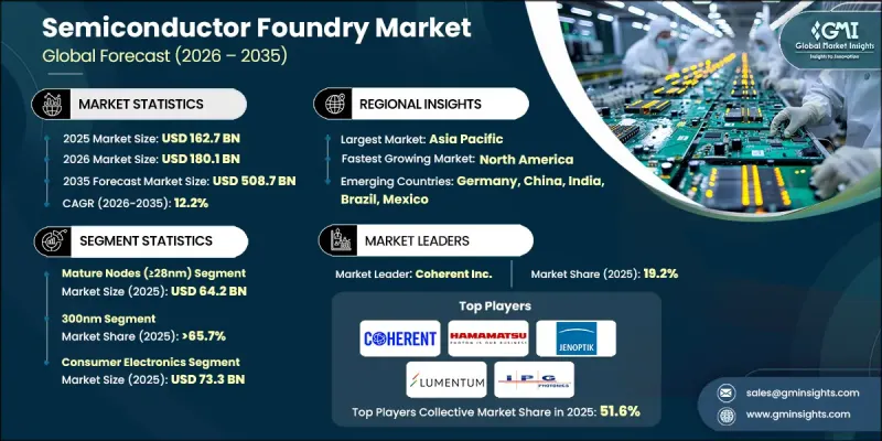
半导体代工厂是专门的製造工厂,利用先进的光刻和精密蚀刻工艺,根据无厂半导体公司提供的设计,在硅晶圆上生产积体电路。纯代工厂模式专注于製造服务,使客户能够加速人工智慧、汽车电子、高效能运算和下一代连接技术领域的创新。对人工智慧驱动系统、电动车和5G基础设施日益增长的需求,使得企业越来越依赖晶片製造外包。代工厂在提供先进节点、支援即时处理以及在复杂的工业环境中实现自动化方面发挥着至关重要的作用。政府和企业对工业4.0和人工智慧基础设施的加大投资,进一步加速了产能的扩张。随着各行业对日益复杂和节能的半导体产品的需求不断增长,半导体代工厂市场也持续扩展其技术能力和全球生产基地,以支持长期的数位转型倡议。
| 市场范围 | |
|---|---|
| 开始年份 | 2025 |
| 预测年份 | 2026-2035 |
| 起始值 | 1627亿美元 |
| 预测金额 | 5087亿美元 |
| 复合年增长率 | 12.2% |
预计到2025年,成熟节点(28奈米以上)市场规模将达到642亿美元,占据最大的市场份额。对汽车半导体、功率元件、工业IoT感测器和类比元件的需求持续推动成熟製程技术的广泛运转率。与更先进的技术相比,这些节点具有成本效益和量产稳定性。同时,製造商正致力于将製程尺寸缩小至2奈米以下,发展晶片架构,并强化封装技术,例如CoWoS和3D整合。供应链扩张措施和永续生产策略也日益成为重要的优先事项。
预计到2025年,300奈米製程製程将占据65.7%的市场份额,并继续保持主导地位。 300奈米製程製造设施的扩建正在提升产能,以满足市场对成熟製程半导体的需求。政府奖励,包括《晶片创新与创新法案》(CHIPS Act)的资金支持,推动了设施升级和地域多角化项目。先进製程製程产能的限制进一步加剧了对类比晶片、电源晶片和传统晶片的需求。市场参与企业正优先考虑2奈米以下製程、晶片整合、供应链多元化、永续性项目以及先进封装解决方案,以满足人工智慧和高效能运算的需求,同时降低地缘政治和资本投资风险。
预计到2025年,北美半导体代工市场占有率将达到29.6%,主要得益于《晶片技术创新与应用法案》(CHIPS Act)带来的巨额投资,以及人工智慧和高效能运算领域对半导体日益增长的需求。国内製造设施的扩建和资料中心容量的提升,正在增强该地区先进节点晶片的生产能力。汽车半导体产量的增加以及降低供应链对亚洲依赖的努力,也为市场成长做出了贡献。製造商正致力于建造能够生产2奈米以下节点晶片、人工智慧加速器晶片和车规级晶片的先进製造设施,同时确保其符合法规要求并具备先进的封装能力。
目录
第一章:调查方法和范围
第二章执行摘要
第三章业界考察
- 生态系分析
- 供应商情况
- 利润率
- 成本结构
- 每个阶段增加的价值
- 影响价值链的因素
- 中断
- 影响产业的因素
- 促进因素
- 对人工智慧和高效能运算的需求日益增长
- 电动车和自动驾驶技术的扩展
- 扩大 5G 和边缘运算的部署
- 先进製程节点(3nm 以下)的进展
- 无晶圆厂半导体经营模式的成长
- 产业潜在风险与挑战
- 对最先进製造流程的高额资本投入
- 地缘政治供应链风险与监管
- 市场机会
- 晶片架构和先进封装
- 铸造厂按地区分類的多元化趋势正在推进。
- 促进因素
- 成长潜力分析
- 监理情势
- 北美洲
- 欧洲
- 亚太地区
- 拉丁美洲
- 中东和非洲
- 波特的分析
- PESTEL 分析
- 科技与创新趋势
- 当前技术趋势
- 新兴技术
- 价格趋势
- 历史价格分析(2022-2024)
- 影响价格趋势的因素
- 区域价格差异
- 价格预测(2026-2035)
- 定价策略
- 新兴经营模式
- 合规要求
第四章 竞争情势
- 介绍
- 企业市占率分析
- 按地区
- 北美洲
- 欧洲
- 亚太地区
- 拉丁美洲
- 中东和非洲
- 市场集中度分析
- 按地区
- 主要企业的竞争标竿分析
- 财务绩效比较
- 收入
- 利润率
- 研究与开发
- 产品系列比较
- 产品线的广度
- 科技
- 创新
- 地理位置比较
- 全球扩张分析
- 服务网路覆盖
- 按地区分類的市场渗透率
- 竞争定位矩阵
- 领导企业
- 受让人
- 追踪者
- 小众玩家
- 战略展望矩阵
- 财务绩效比较
- 2022-2025 年重大发展
- 併购
- 合作伙伴关係和合资企业
- 技术进步
- 扩张和投资策略
- 永续发展倡议
- 数位转型计划
- 新兴/Start-Ups竞争对手的发展趋势
第五章 市场估算与预测:依设备类型划分,2022-2035年
- 晶圆加工设备
- 晶圆处理和自动化设备
- 测量和检测设备
- 组装、包装和测试设备
第六章 市场估计与预测:依技术节点划分,2022-2035年
- 最先进的节点(≤7nm)
- 先进节点(10nm 至 22nm)
- 成熟节点(≥28nm)
第七章 依晶圆尺寸分類的市场估算与预测,2022-2035年
- 200mm
- 300mm
第八章 市场估计与预测:依应用领域划分,2022-2035年
- 家用电子电器
- 沟通
- 车
- 工业的
- 其他的
第九章 半导体代工市场估计与预测:按地区划分,2022-2035年
- 按地区
- 北美洲
- 我们
- 加拿大
- 欧洲
- 英国
- 德国
- 法国
- 义大利
- 西班牙
- 荷兰
- 其他欧洲地区
- 亚太地区
- 中国
- 印度
- 日本
- 韩国
- 澳洲
- 亚太其他地区
- 拉丁美洲
- 巴西
- 墨西哥
- 阿根廷
- 其他拉丁美洲地区
- 中东和非洲
- 沙乌地阿拉伯
- 南非
- 阿拉伯聯合大公国
- 其他中东和非洲地区
第十章:公司简介
- ALPHALAS GmbH
- Coherent Inc.
- CrystaLaser, LLC
- Daheng New Epoch Technology, Inc.
- Edgewave
- Hamamatsu Photonics KK
- Jenoptik Laser GmbH
- Jiangsu Lumispot Technology Co., Ltd.
- Laserglow Technologies
- LASEROPTEK Co., Ltd.
- Lumentum Operations LLC
- LUMIBIRD
- Northrop Grumman Corporation
- Quanta System SpA
- IPG Photonics
The Global Semiconductor Foundry Market was valued at USD 162.7 billion in 2025 and is estimated to grow at a CAGR of 12.2% to reach USD 508.7 billion by 2035.
A semiconductor foundry functions as a specialized manufacturing facility that produces integrated circuits based on designs supplied by fabless companies, using advanced photolithography and precision etching processes on silicon wafers. Pure-play foundry models focus solely on fabrication services, enabling customers to accelerate innovation across artificial intelligence, automotive electronics, high-performance computing, and next-generation connectivity technologies. Rising demand for AI-driven systems, electric vehicles, and 5G infrastructure is strengthening reliance on outsourced chip manufacturing. Foundries play a critical role in delivering advanced nodes, supporting real-time processing, and enabling automation across complex industrial environments. Growing investments in Industry 4.0 and AI infrastructure from both governments and enterprises are further accelerating capacity expansion. As industries require increasingly sophisticated and energy-efficient semiconductors, the semiconductor foundry market continues to expand its technological capabilities and global production footprint to support long-term digital transformation initiatives.
| Market Scope | |
|---|---|
| Start Year | 2025 |
| Forecast Year | 2026-2035 |
| Start Value | $162.7 Billion |
| Forecast Value | $508.7 Billion |
| CAGR | 12.2% |
The mature nodes (>=28nm) segment generated USD 64.2 billion in 2025, representing the largest share of the market. Demand for automotive semiconductors, power devices, industrial IoT sensors, and analog components continues to support strong utilization of mature process technologies. These nodes offer cost efficiency and high-volume manufacturing stability compared to more advanced technologies. At the same time, manufacturers are focusing on scaling sub-2nm processes, advancing chiplet architectures, and enhancing packaging technologies such as CoWoS and 3D integration. Supply chain expansion initiatives and sustainable production strategies are also becoming key priorities.
The 300nm segment accounted for 65.7% share in 2025, maintaining a dominant position within the semiconductor foundry industry. Expansion of 300mm fabrication facilities is increasing production capacity to meet demand for mature-node semiconductors. Facility upgrades and regional diversification programs are being supported by government incentives, including CHIPS Act funding. Constraints in advanced node production are reinforcing demand for analog, power, and legacy chips. Market participants are prioritizing sub-2nm scaling, chiplet integration, diversified supply chains, sustainability programs, and advanced packaging solutions to address AI and high-performance computing requirements while mitigating geopolitical and capital expenditure risks.
North America Semiconductor Foundry Market held a 29.6% share in 2025, driven by substantial CHIPS Act investments and rising demand for AI and high-performance computing semiconductors. Expansion of domestic manufacturing facilities and growing data center capacity are strengthening regional advanced-node output. Increasing automotive semiconductor production and efforts to reduce supply chain dependency on Asia are also contributing to growth. Manufacturers are concentrating on establishing advanced fabrication facilities capable of producing sub-2nm nodes, AI accelerators, and automotive-grade chips, while aligning operations with regulatory compliance and advanced packaging capabilities.
Key companies operating in the Global Semiconductor Foundry Market include ALPHALAS GmbH, Coherent Inc., CrystaLaser, LLC, Daheng New Epoch Technology, Inc., Edgewave, Hamamatsu Photonics K.K., Jenoptik Laser GmbH, Jiangsu Lumispot Technology Co., Ltd., Laserglow Technologies, LASEROPTEK Co., Ltd., Lumentum Operations LLC, LUMIBIRD, Northrop Grumman Corporation, Quanta System S.p.A. and IPG Photonics. Companies in the Semiconductor Foundry Market are reinforcing their competitive position through aggressive capacity expansion, advanced node innovation, and strategic regional investments. Leading players are allocating capital toward sub-2nm research, chiplet ecosystem development, and advanced packaging integration to support AI and high-performance computing applications. Partnerships with fabless design firms and government-backed incentive programs are helping secure long-term production contracts. Firms are also diversifying supply chains to reduce geopolitical risk and enhance operational resilience. Sustainability initiatives, including energy-efficient fabs and reduced water consumption processes, are becoming central to operational strategies.
Table of Contents
Chapter 1 Methodology and Scope
- 1.1 Market scope and definition
- 1.2 Research design
- 1.2.1 Research approach
- 1.2.2 Data collection methods
- 1.3 Data mining sources
- 1.3.1 Global
- 1.3.2 Regional/Country
- 1.4 Base estimates and calculations
- 1.4.1 Base year calculation
- 1.4.2 Key trends for market estimation
- 1.5 Primary research and validation
- 1.5.1 Primary sources
- 1.6 Forecast model
- 1.7 Research assumptions and limitations
Chapter 2 Executive Summary
- 2.1 Industry snapshot
- 2.2 Key market trends
- 2.2.1 Equipment type trends
- 2.2.2 Technology node trends
- 2.2.3 Wafer size trends
- 2.2.4 Application trends
- 2.2.5 Regional trends
- 2.3 TAM Analysis, 2025-2034 (USD Billion)
- 2.4 CXO perspectives: Strategic imperatives
Chapter 3 Industry Insights
- 3.1 Industry ecosystem analysis
- 3.1.1 Supplier Landscape
- 3.1.2 Profit Margin
- 3.1.3 Cost structure
- 3.1.4 Value addition at each stage
- 3.1.5 Factor affecting the value chain
- 3.1.6 Disruptions
- 3.2 Industry impact forces
- 3.2.1 Growth drivers
- 3.2.1.1 Rising demand for AI and high-performance computing
- 3.2.1.2 Expansion of electric vehicles and autonomous driving
- 3.2.1.3 Proliferation of 5G and edge computing deployments
- 3.2.1.4 Advancements in advanced process nodes (sub-3nm)
- 3.2.1.5 Growth in fabless semiconductor business model
- 3.2.2 Industry pitfalls and challenges
- 3.2.2.1 High capital expenditures for leading-edge fabs
- 3.2.2.2 Geopolitical supply chain risks and restrictions
- 3.2.3 Market opportunities
- 3.2.3.1 Chiplet architectures and advanced packaging
- 3.2.3.2 Rise of regional foundry diversification
- 3.2.1 Growth drivers
- 3.3 Growth potential analysis
- 3.4 Regulatory landscape
- 3.4.1 North America
- 3.4.2 Europe
- 3.4.3 Asia Pacific
- 3.4.4 Latin America
- 3.4.5 Middle East & Africa
- 3.5 Porter’s analysis
- 3.6 PESTEL analysis
- 3.7 Technology and innovation landscape
- 3.7.1 Current technological trends
- 3.7.2 Emerging technologies
- 3.8 Price trends
- 3.8.1 Historical price analysis (2022-2024)
- 3.8.2 Price trend drivers
- 3.8.3 Regional price variations
- 3.8.4 Price forecast (2026-2035)
- 3.9 Pricing strategies
- 3.10 Emerging business models
- 3.11 Compliance requirements
Chapter 4 Competitive Landscape, 2025
- 4.1 Introduction
- 4.2 Company market share analysis
- 4.2.1 By Region
- 4.2.1.1 North America
- 4.2.1.2 Europe
- 4.2.1.3 Asia Pacific
- 4.2.1.4 Latin America
- 4.2.1.5 Middle East & Africa
- 4.2.2 Market Concentration Analysis
- 4.2.1 By Region
- 4.3 Competitive benchmarking of key players
- 4.3.1 Financial performance comparison
- 4.3.1.1 Revenue
- 4.3.1.2 Profit margin
- 4.3.1.3 R&D
- 4.3.2 Product portfolio comparison
- 4.3.2.1 Product range breadth
- 4.3.2.2 Technology
- 4.3.2.3 Innovation
- 4.3.3 Geographic presence comparison
- 4.3.3.1 Global footprint analysis
- 4.3.3.2 Service network coverage
- 4.3.3.3 Market penetration by region
- 4.3.4 Competitive positioning matrix
- 4.3.4.1 Leaders
- 4.3.4.2 Challengers
- 4.3.4.3 Followers
- 4.3.4.4 Niche players
- 4.3.5 Strategic outlook matrix
- 4.3.1 Financial performance comparison
- 4.4 Key developments, 2022-2025
- 4.4.1 Mergers and acquisitions
- 4.4.2 Partnerships and collaborations
- 4.4.3 Technological advancements
- 4.4.4 Expansion and investment strategies
- 4.4.5 Sustainability initiatives
- 4.4.6 Digital transformation initiatives
- 4.5 Emerging/ startup competitors landscape
Chapter 5 Market Estimates & Forecast, By Equipment Type, 2022 - 2035 (USD Million)
- 5.1 Key trends
- 5.2 Wafer Processing Equipment
- 5.3 Wafer Handling & Automation Equipment
- 5.4 Metrology & Inspection Equipment
- 5.5 Assembly, Packaging & Test Equipment
Chapter 6 Market Estimates and Forecast, By Technology Node, 2022 - 2035 (USD Million)
- 6.1 Key trends
- 6.2 Leading-Edge Nodes (≤7nm)
- 6.3 Advanced Nodes (10nm-22nm)
- 6.4 Mature Nodes (≥28nm)
Chapter 7 Market Estimates and Forecast, By Wafer Size, 2022 - 2035 (USD Million)
- 7.1 Key trends
- 7.2 200mm
- 7.3 300mm
Chapter 8 Market Estimates and Forecast, By Application, 2022 - 2035 (USD Million)
- 8.1 Key trends
- 8.2 Consumer Electronics
- 8.3 Communication
- 8.4 Automotive
- 8.5 Industrial
- 8.6 Others
Chapter 9 Semiconductor foundry Market Estimates & Forecast, By Region, 2022 - 2035 (USD Million)
- 9.1 Key trends, by region
- 9.2 North America
- 9.2.1 U.S.
- 9.2.2 Canada
- 9.3 Europe
- 9.3.1 UK
- 9.3.2 Germany
- 9.3.3 France
- 9.3.4 Italy
- 9.3.5 Spain
- 9.3.6 Netherlands
- 9.3.7 Rest of Europe
- 9.4 Asia-Pacific
- 9.4.1 China
- 9.4.2 India
- 9.4.3 Japan
- 9.4.4 South Korea
- 9.4.5 Australia
- 9.4.6 Rest of Asia-Pacific
- 9.5 Latin America
- 9.5.1 Brazil
- 9.5.2 Mexico
- 9.5.3 Argentina
- 9.5.4 Rest of Latin America
- 9.6 MEA
- 9.6.1 Saudi Arabia
- 9.6.2 South Africa
- 9.6.3 UAE
- 9.6.4 Rest of MEA
Chapter 10 Company Profiles
- 10.1 ALPHALAS GmbH
- 10.2 Coherent Inc.
- 10.3 CrystaLaser, LLC
- 10.4 Daheng New Epoch Technology, Inc.
- 10.5 Edgewave
- 10.6 Hamamatsu Photonics K.K.
- 10.7 Jenoptik Laser GmbH
- 10.8 Jiangsu Lumispot Technology Co., Ltd.
- 10.9 Laserglow Technologies
- 10.10 LASEROPTEK Co., Ltd.
- 10.11 Lumentum Operations LLC
- 10.12 LUMIBIRD
- 10.13 Northrop Grumman Corporation
- 10.14 Quanta System S.p.A
- 10.15 IPG Photonics
 铸造服务市场:按工艺、客户类型和应用划分-2026-2032年全球市场预测
 半导体代工市场规模、份额和成长分析:按技术节点尺寸、技术、代工类型、应用和地区划分 - 2026-2033 年行业预测
 半导体代工:市场占有率分析、产业趋势与统计、成长预测(2026-2031)
 全球化合物半导体代工服务市场:预测(至2034年)-按材料类型、晶圆尺寸、装置类型、技术、应用、最终用户和地区进行分析
 2026年全球半导体契约製造市场报告
 半导体代工市场-全球产业规模、份额、趋势、机会及预测(依技术节点、应用、地区及竞争格局划分,2021-2031年)
 半导体代工市场规模、占有率、成长、全球产业分析:按类型、应用、区域洞察和预测(2026-2034 年)
 DRAMeXchange 市场情报服务:晶圆代工白金级报告半导体晶圆代工厂市场-2025-2030年预测
 2025-2029年全球半导体代工市场