


 |
市场调查报告书
商品编码
1939646
半导体代工:市场占有率分析、产业趋势与统计、成长预测(2026-2031)Semiconductor Foundry - Market Share Analysis, Industry Trends & Statistics, Growth Forecasts (2026 - 2031) |
||||||
※ 本网页内容可能与最新版本有所差异。详细情况请与我们联繫。
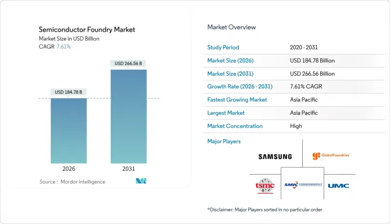
全球半导体代工市场预计到 2026 年将达到 1,847.8 亿美元,高于 2025 年的 1,717.2 亿美元,预计到 2031 年将达到 2,665.6 亿美元。
预计2026年至2031年复合年增长率将达7.61%。
5奈米及以下过程的人工智慧(AI)运算需求激增、成熟製程节点的汽车晶片需求持续成长,以及政府强有力的奖励,共同推动着该产业的技术和地域覆盖范围不断扩大。先进封装技术,特别是晶片组和3D集成电路(3D IC),正逐渐成为重要的收入来源,但水资源管理、出口限制合规以及极紫外光刻(EUV)设备工程师短缺等挑战限制了近期产能扩张。日益激烈的地缘政治竞争正推动北美、欧洲和印度等地的製造业在地化,逐渐削弱亚太地区传统的製造业优势,儘管其主导地位依然稳固。目前的竞争格局聚焦于5奈米及以下製程节点的领先地位、高性价比的28奈米製程能力以及面向Start-Ups的代工即服务(FaaS)产品。
全球半导体代工市场趋势与洞察
面向5奈米以下先进节点的AI加速器竞赛
随着超大规模资料中心业者和晶片设计商竞相训练大规模人工智慧模型,5奈米以下製程的製造能力已从利基市场走向主流。台积电报告称,2025年第二季度,7奈米及更小工艺的晶圆销量占其总销量的74%,这印证了客户对密度优势的重视。三星的2奈米全环栅极製程和英特尔的1.4奈米蓝图凸显了产业向原子级微型化的转型。快速的製程节点转换也加速了对先进中介层的需求,因此需要对晶圆厂和封装生产线进行协同最佳化。高资本密集度(每个晶圆厂超过200亿美元)限制了潜在竞争对手的数量,并巩固了寡占格局,製程技术优势直接决定市场份额。
汽车电气化推动主流晶片需求
电动车需要两卡车的硅:成熟製程节点的电源管理积体电路和尖端製程节点的高效能运算系统级晶片。汽车製造商转向集中式电子架构,确保了28奈米和45奈米製程的长期产能,为经常受到週期性智慧型手机订单压力的晶圆厂提供了可靠的产能补充。漫长的认证週期和严格的AEC-Q100标准促使厂商签订多年产能预订合同,从而改善了那些平衡成熟製程节点和先进製程节点的代工厂的收入前景。特斯拉的客製化晶片策略表明,原始设备製造商(OEM)如何利用专用产能合约来确保供应并实现性能差异化。
地缘政治出口管制的不确定性
针对外国直接产品的出口限制,相关规定扩大,限制了先进光刻技术向某些国家的出口,迫使晶圆厂将传统生产线和先进生产线分开。由于企业需要在多个司法管辖区重复购置设备和审核,合规成本不断上升。在美国的压力下,马来西亚收紧半导体政策,影响波及整个东南亚地区,如今高端GPU的出货都会引发漫长的授权审批流程。难以预测的监管动态阻碍了新计画,尤其是5奈米以下过程的项目,从而延缓了短期投资週期。
细分市场分析
截至2025年,28奈米製程节点将占总收入的59.45%,并构成对成本敏感、大量生产的半导体代工市场规模的基础。 10奈米以下製程节点虽然出货量较小,但预计到2031年将以9.05%的复合年增长率成长,这主要得益于人工智慧和高效能运算的需求。这将导致收入结构两极化:成熟的製程节点将确保汽车和工业领域稳定的现金流,而前缘製程节点则将提供更高的溢价和利润率。
资本支出纪律仍然至关重要。台积电将于2025年开始试生产其2nm工艺,以确保从智慧型手机和加速器客户处获得预付款。英特尔和三星也纷纷推出1.4nm和2nm环栅(GAA)製程开发计划,加剧了资本竞争。同时,16nm和14nm节点将缩小网路晶片的成本绩效差距。传统的65nm及以上製程将继续供应长生命週期的类比和射频设计,即使行动电话需求放缓,也能维持晶圆厂的健康运转率。
向300毫米製造设备的过渡提高了单次运行的晶粒良率,并减少了边缘损耗造成的废弃物,使半导体代工市场到2025年能够占据68.10%的市场份额。随着新建晶圆厂将300毫米设备作为40奈米以下製程的标准配置,复合年增长率将持续维持9.42%的年均水准。同时,200毫米製程已在MEMS、功率GaN和专用模拟应用领域中广泛应用,但这些领域的尺寸缩小和化学特性使得向300毫米製程的过渡充满挑战。
规模经济效应显着。一旦300毫米晶圆厂的月产能达到10万片晶圆,在设备折旧免税额后,其单价可比200毫米晶圆低30%。然而,150亿至200亿美元的进入门槛限制了新进入者,并巩固了现有企业的优势。目前仍有专门的150毫米生产线用于生产碳化硅、砷化镓以及依赖特殊基板的光电产品。
区域分析
预计到2025年,亚太地区将占据22.65%的营收份额,并在2031年之前以8.44%的复合年增长率增长,这主要得益于台湾无与伦比的先进过程节点密度和韩国垂直整合的产业生态系统。台湾在2025年第二季的营收达到288.7亿美元,展现了该地区庞大的生产规模。在出口限制的背景下,中国的中芯国际正专注于28奈米以上製程工艺;而马来西亚和新加坡则在面临美国更严格的限制时,不断提升其组装和测试能力。
在《晶片法案》(CHIPS Act)的推动下,北美正重新崛起为製造地,亚利桑那州、俄亥俄州和纽约州的工厂破土动工,新增了5奈米级和成熟製程节点的产能。联邦津贴降低了数十亿美元计划的风险,而国防抵销协议则保障了最低运作。欧洲则专注于汽车级和专用类比晶片,充分利用德国的汽车产业丛集和荷兰的微影术技术。欧盟的资金规模虽然小规模美国,但目标是到2030年将区域产能翻倍。
在印度、中东和非洲部分地区,该地区正透过对组装、测试和设计服务的激励措施来增强自身影响力。印度斥资100亿美元的计画吸引了美光科技27.5亿美元的ATMP(组装、测试和製造流程)项目以及塔塔集团110亿美元的待开发区项目,其目标是到2030年使国内需求接近1000亿至1100亿美元。海湾国家正在考虑建造晶圆代工厂以实现经济多元化,但水资源限制和技能短缺限制了相关进展。新兴全部区域在寻求缩短供应链,以规避地缘政治衝击。
其他福利:
- Excel格式的市场预测(ME)表
- 3个月的分析师支持
目录
第一章 引言
- 研究假设和市场定义
- 调查范围
第二章调查方法
第三章执行摘要
第四章 市场情势
- 市场概览
- 市场驱动因素
- 汽车电气化推动半导体需求主流化
- 物联网边缘的普及需要成熟的节点容量
- 面向5奈米以下先进节点的AI加速器竞赛
- 晶片组+3D积体电路需要新的代工流程
- 国防部推广可靠的国内製造厂
- 面向Start-Ups的代工厂即服务模式
- 市场限制
- 地缘政治出口管制的不确定性
- 通货膨胀和资本投资的长期投资回收期
- 水资源许可证限制了大型工厂的运营
- 3奈米以下极紫外光刻维护人员短缺
- 产业价值链分析
- 监管环境
- 技术展望
- 晶圆厂运转率趋势
- 波特五力分析
- 供应商的议价能力
- 买方的议价能力
- 新进入者的威胁
- 替代品的威胁
- 竞争对手之间的竞争
- 宏观经济因素如何影响市场
第五章 市场规模与成长预测
- 依技术节点
- 10/7/5 奈米或更小
- 16/14 nm
- 20nm
- 28nm
- 45/40 nm
- 65奈米或以上
- 按晶圆尺寸
- 300 mm
- 200 mm
- 150毫米或更小
- Foundry经营模式
- 全日制
- IDM Foundry 服务
- Fab Light
- 透过使用
- 家用电子电器和通讯设备
- 车
- 工业与物联网
- 高效能运算(HPC)
- 其他用途
- 按地区
- 北美洲
- 我们
- 加拿大
- 墨西哥
- 南美洲
- 巴西
- 阿根廷
- 南美洲其他地区
- 欧洲
- 德国
- 英国
- 法国
- 义大利
- 其他欧洲地区
- 亚太地区
- 中国
- 日本
- 韩国
- 印度
- 亚太其他地区
- 中东
- 沙乌地阿拉伯
- 阿拉伯聯合大公国
- 其他中东地区
- 非洲
- 南非
- 其他非洲地区
- 北美洲
第六章 竞争情势
- 市场集中度
- 策略趋势
- 市占率分析
- 公司简介
- Taiwan Semiconductor Manufacturing Co. Ltd.(TSMC)
- Samsung Electronics Co. Ltd.(Samsung Foundry)
- GlobalFoundries Inc.
- United Microelectronics Corp.(UMC)
- Semiconductor Manufacturing International Corp.(SMIC)
- Intel Corp.(Intel Foundry Services)
- Tower Semiconductor Ltd.
- STMicroelectronics NV
- Powerchip Semiconductor Manufacturing Corp.(PSMC)
- Vanguard International Semiconductor Corp.
- Hua Hong Semiconductor Ltd.
- X-FAB Silicon Foundries SE
- ASE Group
- Dongbu HiTek Co. Ltd.
- Renesas Electronics Corp.
- JCET Group
- Amkor Technology
- SkyWater Technology Inc.
- VIS Semiconductor Co. Ltd.
- PSMC Group(Nexchip)
第七章 市场机会与未来展望
The global semiconductor foundry market size in 2026 is estimated at USD 184.78 billion, growing from 2025 value of USD 171.72 billion with 2031 projections showing USD 266.56 billion, growing at 7.61% CAGR over 2026-2031.
A combination of soaring artificial-intelligence compute needs at sub-5 nm, sustained demand for mature-node automotive chips, and intensive government incentives is widening both the technology and geographic footprint of the sector. Advanced packaging, especially chiplets and 3-D ICs, has become a parallel revenue engine, while water stewardship, export-control compliance, and EUV-tool talent shortages temper near-term capacity additions. Intensifying geopolitical competition is prompting North America, Europe, and India to localize fabrication, gradually diffusing Asia-Pacific's traditional production dominance without dislodging its leadership. Competitive dynamics now hinge on node leadership below 5 nm, cost-efficient 28 nm capacity, and foundry-as-a-service offerings targeting start-ups.
Global Semiconductor Foundry Market Trends and Insights
AI Accelerator Race for Less than 5 nm Advanced Nodes
Sub-5 nm capacity has moved from niche to mainstream as hyperscalers and chip designers race to train larger AI models. TSMC reported that 7 nm and finer nodes contributed 74% of wafer revenue in Q2 2025, underscoring the premium customers place on density leadership. Samsung's gate-all-around 2 nm program and Intel's 1.4 nm roadmap confirm an industry-wide pivot toward atomic-scale geometries. Rapid node migration is also fueling demand for advanced interposers, necessitating co-optimized fab and packaging lines. High capital intensity-often above USD 20 billion per fab-limits viable competitors and cements an oligopolistic market where process leadership directly dictates share.
Mainstream Chip Demand from Automotive Electrification
Electric vehicles require dual-track silicon: power-management ICs at mature nodes and high-compute SoCs at leading nodes. Automakers' shift to centralized electronic architectures locks in long-term 28 nm and 45 nm volumes, providing reliable backfill for fabs otherwise pressured by cyclical smartphone orders. Long qualification cycles and strict AEC-Q100 standards encourage multi-year capacity reservations, improving revenue visibility for foundries that balance mature and advanced nodes. Tesla's custom chip strategy illustrates how OEMs use dedicated capacity deals to secure supply and differentiate performance.
Geopolitical Export-Control Uncertainty
Expanded Foreign-Produced Direct Product rules restrict advanced lithography exports to specific countries, forcing fabs to segregate legacy and cutting-edge lines. Compliance costs rise as companies duplicate equipment sets and audits across jurisdictions. Malaysia's tighter chip policies under U.S. pressure show knock-on effects in Southeast Asia, where routing high-end GPUs now triggers lengthy license reviews. Unpredictable rule-making discourages green-field projects, particularly at 5 nm and below, muting near-term investment cycles.
Other drivers and restraints analyzed in the detailed report include:
- Defense Agencies' Push for Trusted Domestic Fabs
- Chiplets + 3-D IC Needing New Foundry Workflows
- Talent Crunch in Sub-3 nm EUV Maintenance
For complete list of drivers and restraints, kindly check the Table Of Contents.
Segment Analysis
In 2025, the 28 nm node generated 59.45% revenue, anchoring the semiconductor foundry market size for cost-sensitive, high-volume devices. Nodes finer than 10 nm, although smaller in shipment volume, will produce a 9.05% CAGR through 2031, reflecting AI and HPC pull-through. Revenue mix therefore bifurcates: mature nodes assure predictable automotive and industrial cash flows, while leading-edge nodes command premium pricing and margins.
Capex discipline remains pivotal. TSMC begins 2 nm risk production in 2025, drawing prepayments from smartphone and accelerator clients. Intel and Samsung respond with 1.4 nm and 2 nm gate-all-around timelines, intensifying capital races. Meanwhile, 16 nm and 14 nm nodes bridge cost-performance gaps for networking silicon. Legacy 65 nm and above still serve analog and RF designs with long lifecycles, keeping fabs running at healthy utilization even when handset demand softens.
The transition to 300 mm tooling lifted die output per run and cut edge-loss waste, enabling the segment to capture 68.10% of the semiconductor foundry market share in 2025. Growth persists at 9.42% CAGR as new fabs select 300 mm equipment by default for anything below 40 nm. In contrast, 200 mm remains entrenched in MEMS, power GaN, and niche analog where geometry or chemistry complicates 300 mm migration.
Economies of scale are stark. A 300 mm fab reaching 100,000 wafers-per-month can undercut 200 mm cost per die by 30% once fully depreciated. Yet the USD 15-20 billion entry fee restricts newcomers, reinforcing incumbent advantage. Specialized 150 mm lines persist for SiC, GaAs, and photonics products that rely on exotic substrates.
The Semiconductor Foundry Market Report is Segmented by Technology Node (10/7/5 Nm and Below, 16/14 Nm, 20 Nm, and More), Wafer Size (300 Mm, 200 Mm, <=150 Mm), Foundry Business Model (Pure-Play, IDM Foundry Services, Fab-Lite), Application (Consumer Electronics and Communication, Automotive, and More), and Geography (North America, South America, Europe, and More). The Market Forecasts are Provided in Terms of Value (USD).
Geography Analysis
Asia-Pacific captured 22.65% revenue in 2025 and is set for an 8.44% CAGR through 2031, propelled by Taiwan's unrivaled advanced-node density and South Korea's vertical integration ecosystems. Taiwan's Q2 2025 revenue of USD 28.87 billion underscores the region's throughput scale. China's SMIC concentrates on 28 nm and above amid export-tool restrictions, while Malaysia and Singapore reinforce assembly and test depth despite tighter U.S. compliance rules.
North America is re-emerging as a fabrication hub under the CHIPS Act, with groundbreakings in Arizona, Ohio, and New York adding both 5 nm class and mature-node capacity. Federal grants de-risk billion-dollar projects, and defense offsets guarantee baseline loadings. Europe focuses on automotive-grade and specialty analog, leveraging Germany's auto cluster and the Netherlands' lithography prowess. EU funding pools, though smaller than U.S. packages, aim to double regional output by 2030.
India, the Middle East, and pockets of Africa are staking claims via assembly, test, and design-service incentives. India's USD 10 billion program attracted Micron's USD 2.75 billion ATMP and Tata's USD 11 billion green-field fab plans, targeting domestic demand approaching USD 100-110 billion by 2030. Gulf countries explore foundries for economic diversification, but water constraints and skills gaps temper speed. Collectively, new geographies aim to shorten supply chains and hedge geopolitical shocks.
- Taiwan Semiconductor Manufacturing Co. Ltd. (TSMC)
- Samsung Electronics Co. Ltd. (Samsung Foundry)
- GlobalFoundries Inc.
- United Microelectronics Corp. (UMC)
- Semiconductor Manufacturing International Corp. (SMIC)
- Intel Corp. (Intel Foundry Services)
- Tower Semiconductor Ltd.
- STMicroelectronics N.V.
- Powerchip Semiconductor Manufacturing Corp. (PSMC)
- Vanguard International Semiconductor Corp.
- Hua Hong Semiconductor Ltd.
- X-FAB Silicon Foundries SE
- ASE Group
- Dongbu HiTek Co. Ltd.
- Renesas Electronics Corp.
- JCET Group
- Amkor Technology
- SkyWater Technology Inc.
- VIS Semiconductor Co. Ltd.
- PSMC Group (Nexchip)
Additional Benefits:
- The market estimate (ME) sheet in Excel format
- 3 months of analyst support
TABLE OF CONTENTS
1 INTRODUCTION
- 1.1 Study Assumptions and Market Definition
- 1.2 Scope of the Study
2 RESEARCH METHODOLOGY
3 EXECUTIVE SUMMARY
4 MARKET LANDSCAPE
- 4.1 Market Overview
- 4.2 Market Drivers
- 4.2.1 Mainstream chip demand from automotive electrification
- 4.2.2 IoT-edge proliferation requiring mature?node capacity
- 4.2.3 AI accelerator race for Less than 5 nm advanced nodes
- 4.2.4 Chiplets + 3D IC needing new foundry workflows
- 4.2.5 Defense agencies push for trusted domestic fabs
- 4.2.6 Foundry-as-a-Service model for start-ups
- 4.3 Market Restraints
- 4.3.1 Geopolitical export-control uncertainty
- 4.3.2 Capex inflation and long pay-back periods
- 4.3.3 Water-use permits limiting mega-fabs
- 4.3.4 Talent crunch in sub-3 nm EUV maintenance
- 4.4 Industry Value Chain Analysis
- 4.5 Regulatory Landscape
- 4.6 Technological Outlook
- 4.7 Foundry Capacity Utilization Trends
- 4.8 Porter's Five Forces Analysis
- 4.8.1 Bargaining Power of Suppliers
- 4.8.2 Bargaining Power of Buyers
- 4.8.3 Threat of New Entrants
- 4.8.4 Threat of Substitutes
- 4.8.5 Intensity of Competitive Rivalry
- 4.9 Impact of Macroeconomic Factors on the Market
5 MARKET SIZE AND GROWTH FORECASTS (VALUE)
- 5.1 By Technology Node
- 5.1.1 10/7/5 nm and below
- 5.1.2 16/14 nm
- 5.1.3 20 nm
- 5.1.4 28 nm
- 5.1.5 45/40 nm
- 5.1.6 65 nm and above
- 5.2 By Wafer Size
- 5.2.1 300 mm
- 5.2.2 200 mm
- 5.2.3 ?150 mm
- 5.3 By Foundry Business Model
- 5.3.1 Pure-play
- 5.3.2 IDM Foundry Services
- 5.3.3 Fab-lite
- 5.4 By Application
- 5.4.1 Consumer Electronics and Communication
- 5.4.2 Automotive
- 5.4.3 Industrial and IoT
- 5.4.4 High-Performance Computing (HPC)
- 5.4.5 Other Applications
- 5.5 By Geography
- 5.5.1 North America
- 5.5.1.1 United States
- 5.5.1.2 Canada
- 5.5.1.3 Mexico
- 5.5.2 South America
- 5.5.2.1 Brazil
- 5.5.2.2 Argentina
- 5.5.2.3 Rest of South America
- 5.5.3 Europe
- 5.5.3.1 Germany
- 5.5.3.2 United Kingdom
- 5.5.3.3 France
- 5.5.3.4 Italy
- 5.5.3.5 Rest of Europe
- 5.5.4 Asia-Pacific
- 5.5.4.1 China
- 5.5.4.2 Japan
- 5.5.4.3 South Korea
- 5.5.4.4 India
- 5.5.4.5 Rest of Asia-Pacific
- 5.5.5 Middle East
- 5.5.5.1 Saudi Arabia
- 5.5.5.2 United Arab Emirates
- 5.5.5.3 Rest of Middle East
- 5.5.6 Africa
- 5.5.6.1 South Africa
- 5.5.6.2 Rest of Africa
- 5.5.1 North America
6 COMPETITIVE LANDSCAPE
- 6.1 Market Concentration
- 6.2 Strategic Moves
- 6.3 Market Share Analysis
- 6.4 Company Profiles (includes Global level Overview, Market level Overview, Core Segments, Financials as available, Strategic Information, Market Rank/Share, Products and Services, Recent Developments)
- 6.4.1 Taiwan Semiconductor Manufacturing Co. Ltd. (TSMC)
- 6.4.2 Samsung Electronics Co. Ltd. (Samsung Foundry)
- 6.4.3 GlobalFoundries Inc.
- 6.4.4 United Microelectronics Corp. (UMC)
- 6.4.5 Semiconductor Manufacturing International Corp. (SMIC)
- 6.4.6 Intel Corp. (Intel Foundry Services)
- 6.4.7 Tower Semiconductor Ltd.
- 6.4.8 STMicroelectronics N.V.
- 6.4.9 Powerchip Semiconductor Manufacturing Corp. (PSMC)
- 6.4.10 Vanguard International Semiconductor Corp.
- 6.4.11 Hua Hong Semiconductor Ltd.
- 6.4.12 X-FAB Silicon Foundries SE
- 6.4.13 ASE Group
- 6.4.14 Dongbu HiTek Co. Ltd.
- 6.4.15 Renesas Electronics Corp.
- 6.4.16 JCET Group
- 6.4.17 Amkor Technology
- 6.4.18 SkyWater Technology Inc.
- 6.4.19 VIS Semiconductor Co. Ltd.
- 6.4.20 PSMC Group (Nexchip)
7 MARKET OPPORTUNITIES AND FUTURE OUTLOOK
- 7.1 White-space and Unmet-need Assessment
 铸造服务市场:按工艺、客户类型和应用划分-2026-2032年全球市场预测
 半导体代工市场规模、份额和成长分析:按技术节点尺寸、技术、代工类型、应用和地区划分 - 2026-2033 年行业预测
 半导体代工市场:成长机会、成长要素、产业趋势分析及2026年至2035年预测
 全球化合物半导体代工服务市场:预测(至2034年)-按材料类型、晶圆尺寸、装置类型、技术、应用、最终用户和地区进行分析
 2026年全球半导体契约製造市场报告
 半导体代工市场-全球产业规模、份额、趋势、机会及预测(依技术节点、应用、地区及竞争格局划分,2021-2031年)
 半导体代工市场规模、占有率、成长、全球产业分析:按类型、应用、区域洞察和预测(2026-2034 年)
 DRAMeXchange 市场情报服务:晶圆代工白金级报告半导体晶圆代工厂市场-2025-2030年预测
 2025-2029年全球半导体代工市场