


 |
市场调查报告书
商品编码
1433512
薄晶圆加工和切割设备的全球市场:市场占有率分析、行业趋势/统计、成长预测(2024-2029)Thin Wafer Processing and Dicing Equipment - Market Share Analysis, Industry Trends & Statistics, Growth Forecasts (2024 - 2029) |
||||||
※ 本网页内容可能与最新版本有所差异。详细情况请与我们联繫。
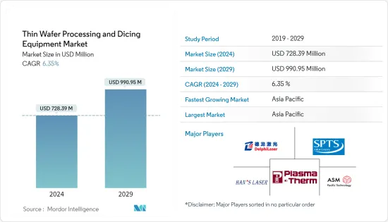
预计2024年全球薄晶圆加工和切割设备市场规模为7.2839亿美元,2029年将达到9.9095亿美元,在预测期内(2024-2029年)复合年增长率为6,预计将增长35 %。
由于使用量的增加,对电子元件的巨大需求促使人们加强努力,使电子封装具有高度的资源效率,使其可用于多种应用。这些因素正在推动半导体和IC封装市场的成长。
主要亮点
- 预计未来几年推动薄晶圆加工和切割设备需求的主要因素之一是其在记忆卡、智慧型手机、智慧卡和各种运算3D电路。 3D电路被用于多种空间受限的应用,如行动家电、感测器、MEMS和工业产品,因为它们提高了整体产品性能,包括高速、耐用、低功耗和轻量化记忆体,越来越普及。
- 随着低成本云端运算解决方案的普及增加了各种企业和产业对伺服器和资料中心系统的使用,对微处理器和数位讯号处理器逻辑装置设备的普及可能会增加。此外,随着支援物联网的连结设备的增加,微处理器的利用率也在增加。这些设备越来越多地采用薄晶圆来实现有效的热管理并提高性能。所有这些原因都在推动逻辑装置市场的扩张。
- 多年来,硅晶圆一直被用作微电子和 MEMS 的製造平台。绝缘体上硅基基板是标准硅晶圆的独特变体。为了製造这种晶圆,需要使用大约 1 至 2 公尺厚的二氧化硅黏合层将两个硅晶圆黏合在一起。单片晶圆被压平至10至50公尺的厚度。涂层的确切厚度取决于应用。
- 建造最先进的薄晶圆代工厂的成本呈指数级上升,对产业带来压力。半导体製造商现在已经集中。随着性能提昇放缓,特种薄晶圆变得越来越有吸引力。使薄晶圆无所不在的设计决策对于某些运算任务来说可能不是最佳的。
- 由于全球工业和汽车电子产品的需求放缓,并因 COVID-19 大流行而加剧,该市场的企业发展商的薄晶圆半导体订单有所下降。
薄晶圆加工切割设备市场趋势
对半导体小型化的需求不断增长正在推动市场发展
- 家用电器、医疗保健和汽车等领域对小型电子设备的需求不断增长,迫使半导体 IC 製造商缩小其 IC 尺寸。因此,预计在预测期内市场将缩小,需求将激增。
- 从地区来看,无晶圆厂经营模式是亚洲国家在全球半导体销售中占据突出地位的关键因素。无厂半导体公司通常将製造业务委託给晶圆代工厂、组装和测试 (OSAT) 公司。根据半导体产业协会(SIA)发布的报告,2021年美国的主导地位自1990年以来显着下降,仅占半导体製造能力的12%。东亚特别是中国的崛起得益于各国政府提供的各种奖励和补贴。
- FUJIFILM表示,由于人工智慧、物联网、下一代通讯标准5G的广泛使用以及自动驾驶技术的进步,预计半导体的需求将进一步增加,性能将得到改善,因此半导体装置的小型化仍在继续。由于上述因素,对小型轻量消费设备的需求不断增长,这些设备依赖于超薄硅晶圆上构建的3D电路架构,并有望提供峰值性能。
- 该晶圆非常薄且平坦。同时,小型化产生了在单一晶片上整合多种功能的需求。晶圆尺寸的不断增大(直径高达 12 吋)正在推动晶圆技术的新趋势。
- 2021 年 5 月,IBM 宣布在半导体设计和加工方面取得突破,发明了首款采用 2 奈米 (nm) 奈米片技术的晶片。半导体应用广泛,包括电脑、消费性电子产品、通讯设备、运输系统和关键基础设施。尤其是在混合云端、AI、物联网时代,对晶片效能和能源效率有着强烈的需求。 IBM 创新的 2nm 晶片技术推进了半导体产业的最尖端科技,以满足这种不断增长的需求。 IBM 的 2nm 晶片技术预计将比目前最先进的 7nm 晶片提供 45% 的性能提升和 75% 的能耗降低。
亚太地区占最大市场占有率份额
- 亚太地区是全球最大且成长最快的半导体市场。中国、韩国和新加坡等国家对智慧型手机和其他消费性电子产品的庞大需求鼓励许多供应商在该地区设立生产基地。
- 该市场上的众多中国企业正致力于透过收购和合併来扩大业务。例如,2021年8月,WaferTech透过其荷兰子公司Nexperia以约6,300万欧元收购了Newport Wafer Fab。根据闻泰向上海证券交易所提交的声明,此次收购于 7 月宣布,并确认了交易条款。闻泰科技是一家组装智慧型手机和其他家用电器的上市製造商。
- 日本拥有多家主要製造商和电子产业,在半导体产业中占有不可或缺的地位。预计政府将启动一项研究,评估主要晶片製造商向该国扩张的可能性。同时,总部位于日本的组织被认为是半导体製造和封装中消耗的大多数关键材料的主要供应商。对于日本供应商来说,日本的外汇和高生产成本使得材料更加昂贵,并为其他低端应用供应商提供了商机。
- 在澳大利亚,电子製造业的成长以及各种最终用途行业越来越多地采用先进设备正在影响市场的成长。电视和智慧型手机的销售主要推动家用电器的成长。
- 2021年10月,Quad Alliance还在澳洲、印度、美国和日本发起了半导体供应链倡议,旨在绘製半导体及其关键零件的产能分布图、识别漏洞并加强供应链安全。与新南威尔斯州半导体产业服务管理局一起,这些是将澳洲打造为亚太地区参与者并确保我们在全球半导体供应链中的地位的正确步骤。
- 目前,印度的半导体需求主要透过进口来满足。因此,需要对奖励链进行激励,使印度在经济上自力更生,在技术上处于领先地位。 2021 年 12 月,政府设想实施一项预算超过 7,600 万印度卢比的综合计划,以发展印度的半导体和显示器製造生态系统。新计画下的财政支持力道达2.3亿印度卢比,涵盖电气设备等整个供应链。
- 全自动驾驶汽车的成长轨迹将取决于亚太地区的因素,包括技术进步、消费者接受全自动驾驶汽车的意愿、定价以及供应商和OEM解决关键车辆安全问题的能力,这些都将受到很大影响。由于这些因素,汽车和半导体产业不断致力于增强技术、协商原材料价格,并最终将汽车与可靠的技术结合。
薄晶圆加工及切割设备产业概况
薄晶圆加工和切割设备市场仅由少数几家主要公司组成,包括DISCO、Panasonic、日本和台湾脉衝马达。此外,市场在薄晶圆製造流程方面仍面临重大挑战。上述因素也导致新参与企业进入市场的延迟。然而,市场参与者不断的创新和研发努力保持了竞争力。因此,估计当前市场上竞争公司之间的敌意是温和的。
- 2022 年 4 月 - DISCO 公司宣布获得英特尔 EPIC 杰出供应商奖。该奖项旨在表彰在所有绩效标准上始终如一的高水准绩效。
- 2022年1月-总部位于东京的横河电机公司与沙乌地阿美公司签署了一份谅解备忘录,探讨在沙乌地阿拉伯王国实现半导体晶片製造在地化的可能性。
其他福利:
- Excel 格式的市场预测 (ME) 表
- 3 个月分析师支持
目录
第一章简介
- 研究假设和市场定义
- 调查范围
第二章调查方法
第三章执行摘要
第四章市场洞察
- 市场概况
- 市场促进与市场约束因素介绍
- 产业吸引力:波特五力分析
- 新进入者的威胁
- 买方议价能力
- 供应商的议价能力
- 替代品的威胁
- 竞争公司之间敌对关係的强度
- 产业价值链分析
- COVID-19 市场影响评估
第五章市场动态
- 市场驱动因素
- 对智慧卡、RFID 技术和汽车电源 IC 的需求增加
- 对半导体小型化的需求日益增长
- 市场限制因素
- 製造挑战
第六章市场区隔
- 依设备类型
- 细化装置
- 刮片设备
- 刀片切割
- 雷射消熔
- 隐形切割
- 等离子切割
- 按用途
- 记忆体逻辑 (TSV)
- 微机电系统元件
- 功率元件
- CMOS影像感测器
- RFID
- 晶圆厚度趋势
- 按晶圆尺寸
- 小于4英寸
- 5寸和6寸
- 8吋
- 12寸
- 按地区
- 北美洲
- 美国
- 加拿大
- 欧洲
- 英国
- 德国
- 法国
- 西班牙
- 义大利
- 其他欧洲国家
- 亚太地区
- 中国
- 日本
- 澳洲
- 印度
- 其他亚太地区
- 拉丁美洲
- 墨西哥
- 巴西
- 其他拉丁美洲
- 中东/非洲
- 南非
- 沙乌地阿拉伯
- 其他中东/非洲
- 北美洲
第七章 竞争形势
- 公司简介
- Suzhou Delphi Laser Co. Ltd
- SPTS Technologies Limited
- Plasma-Therm LLC
- Han's Laser Technology Industry Group Co. Ltd
- ASM Laser Separation International(ALSI)BV
- Disco Corporation
- Tokyo Seimitsu Co, Ltd.(Accretech)
- Neon Tech Co. Ltd.
- Advanced Dicing Technologies Ltd
- Panasonic Corporation
第八章投资分析
第九章 市场机会及未来趋势
The Thin Wafer Processing and Dicing Equipment Market size is estimated at USD 728.39 million in 2024, and is expected to reach USD 990.95 million by 2029, growing at a CAGR of 6.35% during the forecast period (2024-2029).
The increasing efforts to make electronic packaging highly resourceful due to the enormous demand for electronic components owing to amplified usage have made electronic packaging useful in a myriad of applications. These factors are driving the growth of the semiconductor and IC packaging market.
Key Highlights
- One of the major factors expected to boost the demand for thin wafer processing and dicing equipment in the coming years is the growing demand for three-dimensional integrated circuits, which are widely used in miniature semiconductor devices such as memory cards, smartphones, and smart cards, and various computing devices. Three-dimensional circuits are becoming more popular in multiple space-constrained applications, such as portable consumer electronics, sensors, MEMS, and industrial products because they improve overall product performance in terms of speed, durability, low power consumption, and lightweight memory.
- The expanding use of server and data center systems across various enterprises and industries, due to the widespread availability of low-cost cloud computing solutions, is likely to fuel demand for logic devices like microprocessors and digital signal processors. In addition, as the number of IoT-enabled linked devices grows, the utilization of microprocessors also increases. Thin wafers are increasingly employed in these devices to enable effective temperature management and enhance performance. All of these reasons are assisting in expanding the logic device market.
- Silicon wafers have long been used as a fabrication platform in microelectronics and MEMS. The silicon-on-insulator substrate is a unique variation of the standard silicon wafer. Two silicon wafers are glued together using a bond layer of silicon dioxide with a thickness of about 1-2 m to make these wafers. One silicon wafer gets flattened down to 10-50 m in thickness. The application will determine the exact thickness of the coating.
- The cost of building state-of-the-art thin wafer foundries has increased exponentially, which puts pressure on the industry. This is where the number of semiconductor manufacturers was consolidated in recent times. Performance boosts are slowing down, making specialized thin wafers increasingly attractive. The design decisions that enable thin wafers to be universal may be sub-optimal for some computing tasks.
- Due to the global slowdown in demand in the industrial and automotive electronics sectors that the COVID-19 pandemic has worsened, manufacturers operating in the market have registered a decline in orders for Thin Wafer semiconductors.
Thin Wafer Processing & Dicing Equipment Market Trends
Increasing Need for Miniaturization of Semiconductors to Drive the Market
- Due to increasing demand for compact electronic devices in segments such as consumer electronics, healthcare, and automotive, semiconductor IC manufacturers are forced to reduce the size of ICs. It has, therefore, given rise to miniaturization in the market, which is expected to experience a surge in its demand during the forecast period.
- Across geographies, the fabless business model is the major contributor to the prominent position of various Asian countries in semiconductor sales across the world. Fabless firms typically outsource fabrication to pure-play foundries and outsourced assembly and test (OSAT) firms. According to the report published by the Semiconductor Industry Association (SIA), in 2021, the dominance of the United States has decreased severely from 1990 and accounted for only 12% of the semiconductor manufacturing capacity. The rise of East Asia, especially China, is credited to various incentives and subsidies offered by the governments of various countries.
- According to Fujifilm, the miniaturization of semiconductor devices continues as the increasing use of AI, IoT, next-generation communication standard '5G', and the advancement of autonomous driving technology are expected to increase further demand and performance boost for semiconductors. The factors mentioned above have led to the rise in demand for small and lightweight consumer devices that rely on 3D circuit architecture built onto ultra-thin silicon wafers in order to perform at peak capacity.
- These wafers are extremely thin and flat. At the same time, miniaturization has resulted in the need to integrate several features on a single chip. Due to the large-sized wafers (with a diameter of up to 12 inches), there is a new trend in wafer technology.
- In May 2021, with the invention of the first chip using 2 nanometers (nm) nanosheet technology, IBM announced a breakthrough in semiconductor design and process. Semiconductors are used in a wide range of applications, including computers, appliances, communication devices, transportation systems, and critical infrastructure. Chip performance and energy efficiency are in high demand, particularly in the age of hybrid cloud, AI, and the Internet of Things. IBM's innovative 2 nm chip technology contributes to advancing the semiconductor industry's state-of-the-art, answering this expanding demand. It's expected to deliver 45% better performance and 75% lower energy consumption than today's most advanced 7 nm node chips.
Asia Pacific to Hold the Largest Market Share
- The Asia Pacific is the largest and fastest-growing semiconductor market in the world. Significant demand for smartphones and other consumer electronics devices from countries such as China, the Republic of Korea, and Singapore, are encouraging many vendors to set up production establishments in the region.
- China's various players in the market are focusing on expanding business through acquisitions and mergers. For instance, in August 2021, Wingtech acquired Newport Wafer Fab for around EUR 63 million through a Dutch subsidiary called Nexperia. The deal was announced in July, confirming the terms of the agreement, according to a Wingtech statement filed with the Shanghai Stock Exchange. Wingtech is a listed manufacturer that assembles smartphones and other home appliances.
- Japan occupies an essential position in the semiconductor industry as it is home to several major manufacturers and the electronics industry. The government is expected to begin an investigation to assess the potential for bringing major chip makers into the country. Meanwhile, Japan-based organizations are considered the significant suppliers of most of the critical materials consumed in semiconductor manufacturing and packaging. For Japanese-based suppliers, Japanese exchange rates and high production costs make materials more expensive and open up opportunities for other suppliers for low-end applications.
- In Australia, the growing electronics manufacturing sector and the increasing adoption of advanced devices among various end-user industries are influencing the market growth. The sales of televisions and smartphones have primarily driven the growth in consumer electronics.
- In October 2021, in Australia, India, the United States, and Japan, the Quad Alliance also launched a semiconductor supply chain initiative aimed at capacity mapping, vulnerability identification, and enhanced supply chain security for semiconductors and their critical components. Together with NSW's Semiconductor Sector Service Bureau, these are the proper steps to establish Australia as a player in the Asia Pacific region and secure its position in the global semiconductor supply chain.
- Currently, India's semiconductor demand is majorly met by imports. Therefore, it was necessary to incentivize the value chain to make India economically independent and technologically leading. The government envisioned a comprehensive program in December 2021 to develop India's semiconductor and display manufacturing ecosystem with a budget of over INR 76,000 crores. Financial support efforts under the new program amounted to INR 230,000, covering the entire electrical device supply chain and more.
- The growth trajectory of fully-autonomous automobiles is heavily influenced by factors in Asia-Pacific, including technology advancements, consumer willingness to accept fully-automated vehicles, pricing, and suppliers' and OEMs' capacity to address significant concerns about vehicles safety. According to these factors, the automotive and semiconductor industries are always concentrating on enhancing technologies, negotiating raw material prices, and finally combining cars with reliable technology.
Thin Wafer Processing & Dicing Equipment Industry Overview
The market for thin wafer processing and dicing comprises very few major players, such as Disco Corporation, Panasonic Corporation, Nippon, and Pulse Motor Taiwan. Moreover, the market still faces considerable challenges in the manufacturing processes of thin wafers. The above-mentioned factor also led to a slower entry of new players into the market. Nevertheless, constant innovations and R&D efforts by the players in the market maintain a competitive edge. Therefore, competitive rivalry in the market at present is rated moderate.
- April 2022 - DISCO Corporation has announced that it has been awarded Intel's EPIC Distinguished Supplier Award. This award distinguishes a consistent level of robust performance across all performance criteria.
- January 2022 - Tokyo-based Yokogawa Electric Corporation signed a memorandum of understanding with Aramco for collaboration to explore potential opportunities for localizing semiconductor chip manufacturing in the Kingdom of Saudi Arabia.
Additional Benefits:
- The market estimate (ME) sheet in Excel format
- 3 months of analyst support
TABLE OF CONTENTS
1 INTRODUCTION
- 1.1 Study Assumptions and Market Definition
- 1.2 Scope of the Study
2 RESEARCH METHODOLOGY
3 EXECUTIVE SUMMARY
4 MARKET INSIGHTS
- 4.1 Market Overview
- 4.2 Introduction to Market Drivers and Restraints
- 4.3 Industry Attractiveness Porter's Five Forces Analysis
- 4.3.1 Threat of New Entrants
- 4.3.2 Bargaining Power of Buyers
- 4.3.3 Bargaining Power of Suppliers
- 4.3.4 Threat of Substitute Products
- 4.3.5 Intensity of Competitive Rivalry
- 4.4 Industry Value Chain Analysis
- 4.5 Assessment of the Impact of COVID-19 on the Market
5 MARKET DYNAMICS
- 5.1 Market Drivers
- 5.1.1 Increasing Demand for Smart Cards, RFID Technology, and Automotive Power ICs
- 5.1.2 Increasing Need for Miniaturization of Semiconductors
- 5.2 Market Restraints
- 5.2.1 Manufacturing Challenges
6 MARKET SEGMENTATION
- 6.1 By Equipment Type
- 6.1.1 Thinning Equipment
- 6.1.2 Dicing Equipment
- 6.1.2.1 Blade Dicing
- 6.1.2.2 Laser Ablation
- 6.1.2.3 Stealth Dicing
- 6.1.2.4 Plasma Dicing
- 6.2 By Application
- 6.2.1 Memory and Logic (TSV)
- 6.2.2 MEMS Devices
- 6.2.3 Power Devices
- 6.2.4 CMOS Image Sensors
- 6.2.5 RFID
- 6.3 By Wafer Thickness Trends
- 6.4 By Wafer Size
- 6.4.1 Less than 4 inch
- 6.4.2 5 inch and 6 inch
- 6.4.3 8 inch
- 6.4.4 12 inch
- 6.5 By Geography
- 6.5.1 North America
- 6.5.1.1 United States
- 6.5.1.2 Canada
- 6.5.2 Europe
- 6.5.2.1 United Kingdom
- 6.5.2.2 Germany
- 6.5.2.3 France
- 6.5.2.4 Spain
- 6.5.2.5 Italy
- 6.5.2.6 Rest of Europe
- 6.5.3 Asia-Pacific
- 6.5.3.1 China
- 6.5.3.2 Japan
- 6.5.3.3 Australia
- 6.5.3.4 India
- 6.5.3.5 Rest of Asia-Pacific
- 6.5.4 Latin America
- 6.5.4.1 Mexico
- 6.5.4.2 Brazil
- 6.5.4.3 Rest of Latin America
- 6.5.5 Middle-East and Africa
- 6.5.5.1 South Africa
- 6.5.5.2 Saudi Arabia
- 6.5.5.3 Rest of Middle-East and Africa
- 6.5.1 North America
7 COMPETITIVE LANDSCAPE
- 7.1 Company Profiles
- 7.1.1 Suzhou Delphi Laser Co. Ltd
- 7.1.2 SPTS Technologies Limited
- 7.1.3 Plasma-Therm LLC
- 7.1.4 Han's Laser Technology Industry Group Co. Ltd
- 7.1.5 ASM Laser Separation International (ALSI) B.V.
- 7.1.6 Disco Corporation
- 7.1.7 Tokyo Seimitsu Co, Ltd. (Accretech)
- 7.1.8 Neon Tech Co. Ltd.
- 7.1.9 Advanced Dicing Technologies Ltd
- 7.1.10 Panasonic Corporation
8 INVESTMENT ANALYSIS
9 MARKET OPPORTUNITIES AND FUTURE TRENDS
 全球雷射开槽设备市场按雷射类型、製程类型、操作类型、产出能力、应用和最终用途行业划分 - 预测 2025-2030 年
 薄晶圆加工和切割设备市场,按产品类型、晶圆尺寸、晶圆厚度、应用、最终用户、国家和地区划分 - 2025 年至 2032 年全球行业分析、市场规模、市场份额和预测
 晶圆加工设备市场 - 全球产业规模、份额、趋势、机会和预测,按製程、应用、最终用户、地区和竞争细分,2020-2030 年预测
 晶圆加工和组装设备全球市场:市场占有率分析、行业趋势和统计、成长预测(2025-2030 年)
 晶圆处理设备的全球市场:市场规模·占有率·趋势,产业分析 (各工程·各用途·各终端用户·各地区),未来预测 (2025年~2034年)
 晶圆加工设备市场:按产品类型、应用、最终用户、技术节点划分 - 2025-2030 年全球预测
 单晶圆加工设备市场:按设备类型、应用、技术和最终用户 - 2025-2030 年全球预测
 薄晶圆加工和切割设备市场机会、成长驱动因素、产业趋势分析与预测 2024 - 2032 年
 晶圆加工设备市场规模、份额、趋势分析报告:按製程、按应用、按地区、细分市场预测,2024-2030
 晶圆雷射拉霸机市场预测至 2030 年:按类型、晶圆尺寸、应用、最终用户和地区进行的全球分析