


 |
市场调查报告书
商品编码
1433926
扇出封装:市场占有率分析、产业趋势与统计、成长预测(2024-2029)Fan Out Packaging - Market Share Analysis, Industry Trends & Statistics, Growth Forecasts (2024 - 2029) |
||||||
※ 本网页内容可能与最新版本有所差异。详细情况请与我们联繫。
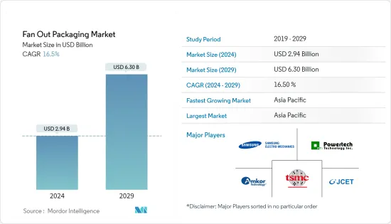
扇出封装市场规模预计到 2024 年为 29.4 亿美元,预计到 2029 年将达到 63 亿美元,在预测期内(2024-2029 年)复合年增长率为 16.5%
该市场的扩张是由半导体技术的进步和各行业需求的快速成长所推动的。
主要亮点
- 由于对高性能、节能、薄型和小尺寸封装的要求,扇出晶圆层次电子构装(FOWLP) 在智慧型手机等占地面积敏感的设备中得到越来越多的使用。此外,现代智慧型手机平均采用 5-7 个晶圆级封装(尤其是扇出封装),而且这一数字预计未来还会增加。这是因为传统的堆迭封装(PoP)记忆体逻辑解决方案正在逐渐被取代。
- 此外,人工智慧和机器学习在各个领域的应用不断增加,也增加了高效能运算在市场上的采用。超高清扇出技术预计将应用于云端、5G、自动驾驶汽车和人工智慧晶片,并将在预测期内引领封装趋势。
- 韩国半导体产业正在努力改进并使 3D TSV(硅穿孔)、封装、FoWLP(扇出晶圆级封装)和 FoPLP(扇出面板级封装)技术更加有效。提高半导体性能,提高整合度。
- 2021 年 12 月,Nepes Laweh Corporation 宣布已利用 Deca 的 M 系列扇出技术成功製造出全球首款 600 mm x 600 mm 大型面板级封装 (PLP)。根据该公司介绍,扇出面板级封装(FOPLP)线已于第三季通过客户认证,建立稳定的产量比率,并开始全面量产。
- 由于韩国公司迄今为止在这些系统上依赖外国公司,KOSTEK 预计未来进口替代效应将显着。在扇出封装过程中可以使用临时晶圆键合机和脱键合技术。
- 由于冠状病毒感染疾病(COVID-19)的爆发,由于货物流动受到限制以及半导体供应链的严重中断,半导体封装市场成长放缓。 2020 年第一季,COVID-19 降低了半导体供应商和分销通路客户的存量基准。新型冠状病毒的传播预计将对市场产生长期影响。
扇出型封装市场趋势
透过高密度扇出获得较大份额
- 高中阶扇出,适用于每平方毫米 6 至 12 个 I/O 和 15/15μm 至 5/5μm 线路/空间的中端到高阶应用。高密度扇出封装已变得流行,以适应行动电话封装的外形尺寸和性能要求。此技术的主要组成部分包括线路重布(RDL)金属和巨型柱电镀。
- 台积电的 InFO 技术是高密度扇出最着名的例子之一。此技术针对高引脚数应用,例如应用处理器 (AP)。该公司计划将其 FO-WLP 领域扩展到 inFO-Antenna-in-Package (AiP) 和 inFO-on-Substrate 等技术。这些包装用于汽车、伺服器、智慧型手机等。苹果是这项新技术的早期采用者之一,在 2016 年底发布的 iPhone 7 的 A10 应用处理器中使用了该技术。
- 由于这些优势,高通和联发科于 2021 年 12 月宣布,将采用扇出 PoP 来製造其旗舰智慧型手机应用处理器,效仿苹果采用台积电 InFO_PoP 技术封装其 iPhone 晶片的脚步。
- 此外,半导体市场的成长以及高密度扇出封装解决方案的发展预计将推动预测期内的市场成长。例如,2021年7月,全球领先的复合电路製造商和技术解决方案供应商长电科技正式推出了其用于XDFOI晶片的全系列超高密度扇出封装选项。一种有效的、高密度连接、高密度、高可靠性的晶片异构整合解决方案。
- 高密度扇出晶圆层次电子构装(FOWLP) 的生产也取得了进展。正在开发的解决方案旨在缩小晶片尺寸/高度并降低製造成本,同时提高可靠性、能源效率、设备速度和多功能整合。例如,SPTS Technologies 为领先的半导体封装公司提供多种等电浆蚀刻和沈积製程技术,用于高密度扇出晶圆级封装等先进封装方案。
- 此外,晶圆级处理的製造能力与使用高铜 (Cu) 柱和直通封装等贯穿模製互连件创建 3D 结构的能力相结合,使高密度扇出 (HDFO) 封装成为可能。 ,可以满足这些小型化的需求。过孔(TPV)和先进的覆晶构装技术。
台湾占有较大市场份额
- 台湾是许多主要半导体製造公司的所在地,推动了对先进半导体封装(尤其是 PLP)的需求。据政府智库科技国际战略中心称,2021年台湾的产出预计将成长25.9%,达到1,470亿美元。
- 根据半导体行业协会 (SIA) 的数据,亚太地区的半导体销售额占全球半导体销售额的 50% 以上。这使台湾供应商有机会为越来越多的半导体应用提供 FOWLP。
- 国内大部分企业都扩大了扇出型封装产能,可望进一步增加出口,有利于开拓国内市场。例如,最近宣布重返晶圆代工厂产业的英特尔也将在新墨西哥州投资35亿美元建造半导体封装工厂,计划于2022年下半年开始运作。
- 此外,2021年6月,纯半导体后处理(OAST)公司日月光开始投资先进封装设备,以应对半导体供需短缺的情况。我们透过从HANMI Semiconductor购买大量用于WLP和PLP製程的半导体製造设备来加速我们的业务扩张。
- 此外,第五代 (5G) 无线通讯和高效能运算市场的成长使製造商能够开发新技术。例如,作为高密度扇出领域的唯一领导者,台积电计划将 FO-WLP 领域扩展到 inFO-天线封装 (AiP) 和 inFO-on-Substrate (oS) 等技术。我是。
扇出型封装产业概述
市场适度分散,参与者多。全球扇出型封装市场的主要企业包括台积电、江苏长电、Amkor Technology Inc.、三星马达、力成科技等。这些参与者热衷于产品创新、併购和收购等发展,以增加市场占有率。
- 2021 年 11 月 - 半导体封装和测试服务供应商 Amkor Technology, Inc. 宣布有意在越南北宁省建设智慧工厂。提案工厂的初始阶段将专注于为世界领先的半导体和电子製造公司提供先进的系统级封装(SiP)组装和测试服务。
- 2021 年 2 月 - 三星晶圆代工厂已向亚利桑那州、纽约州和德克萨斯当局提交文件,寻求在美国建立最先进的半导体製造工厂。该工厂可能建在德克萨斯州奥斯汀附近,预计耗资超过 170 亿美元,并创造 1,800 个就业机会。预计2023年第四季上线。
其他福利
- Excel 格式的市场预测 (ME) 表
- 3 个月分析师支持
目录
第一章简介
- 研究假设和市场定义
- 调查范围
第二章调查方法
第三章执行摘要
第四章市场洞察
- 市场概况
- 产业吸引力-波特五力分析
- 供应商的议价能力
- 买方议价能力
- 新进入者的威胁
- 竞争公司之间的敌对关係
- 替代品的威胁
- COVID-19 对市场的影响
第五章市场动态
- 市场驱动因素
- 高效能运算和5G无线网路的普及
- 市场限制因素
- 与製造相关的製造成本问题
- FOPLP市场机会
- COVID-19 对市场的影响
第六章市场区隔
- 按类型
- 核心扇出
- 高密度扇出
- 超密集扇出
- 依运营商类型
- 200 mm
- 300 mm
- 控制板
- 按经营模式
- OSAT
- 铸造厂
- IDM
- 按地区
- 台湾
- 中国
- 美国
- 韩国
- 日本
- 欧洲
第七章 扇出封装厂商排名分析
第八章 竞争形势
- 公司简介
- Taiwan Semiconductor Manufacturing Company Limited
- Jiangsu Changjiang Electronics Tech Co.
- Samsung Electro-Mechanics
- Powertech Technology Inc.
- Amkor Technology Inc.
- Advanced Semiconductor Engineering Inc
- Nepes Corporation
第九章投资分析
第10章 未来展望
The Fan Out Packaging Market size is estimated at USD 2.94 billion in 2024, and is expected to reach USD 6.30 billion by 2029, growing at a CAGR of 16.5% during the forecast period (2024-2029).
The expansion of this market is being driven by technological advancements in semiconductor-based technologies and rapidly expanding demand in various sectors.
Key Highlights
- Fan-out wafer level packaging (FOWLP) finds its increased application in footprint-sensitive devices such as smartphones due to the requirement of high-performing, energy-efficient thin- and small-form-factor packages. Further, on average, five to seven wafer-level packages (especially fan-out) can be found in modern smartphones, and the numbers are expected to increase in the future. This is because they are gradually replacing the more traditional package-on-package (PoP) memory-on-logic solutions.
- Moreover, the increasing application of artificial intelligence and machine learning in various fields has increased the installation of high-performance computing in the market. UHD fan-out technology is expected to be applied to the cloud, 5G, autonomous cars, and AI chips and will lead the packaging trend during the forecast period.
- South Korea's semiconductor industry is continuing to put in efforts to improve and make 3D TSV (Through-silicon via), packaging and FoWLP (Fan-out Wafer-Level Packaging), and FoPLP (Fan-out Panel-Level Packaging) technologies more effective to raise the performance of semiconductors and the degree of integration.
- In December 2021, Nepes Laweh corporation announced the successful production of the world's first 600 mm x 600 mm large Panel Level Packaging (PLP) using Deca's M-Series fan-out technologies. The Fan-out-Panel Level Packaging (FOPLP) line passed customer certification in the third quarter, established a consistent yield, and commenced full-scale mass production, according to the business.
- Because South Korean companies depended on foreign companies for these systems in the past, KOSTEK is expecting a huge import substitution effect in the future. Its temporary wafer bonder and debonding techniques can be used during a fan-out packaging process.
- With the outbreak of COVID-19, the semiconductor packaging market witnessed a decline in growth due to restrictions on the movement of goods and severe disruptions in the semiconductor supply chain. In Q1 2020, COVID-19 caused low inventory levels for clients of semiconductor vendors and distribution channels. The market is expected to witness a long-term impact due to the coronavirus outbreak.
Fan Out Packaging Market Trends
High-Density Fan-Out to Hold a Significant Share
- Targeted for mid-range to high-end apps, high-density fan-out has between 6 to 12 I/Os per mm2 and between 15/15 μm to 5/5 μm line/space. High-density fan-out packaging gained popularity to address the form factor and performance requirements for mobile phone packaging. Key building blocks for this technology comprise redistribution layer (RDL) metal and mega pillar plating.
- TSMC's InFO technology is one of the most notable examples of high-density fan-out. This technology targets higher pin count applications, such as application processors (AP). The company plans to extend its FO-WLP segment into technologies like inFO-Antenna-in-Package (AiP) and inFO-on-Substrate. These packages are used in automobiles, servers, and smartphones. Apple was one of the early adopters of this new technology, which used it in the A10 application processor of the iPhone 7, introduced in late 2016.
- Owing to such benefits, in December 2021, Qualcomm and MediaTek both considered adopting fan-out PoP in the production of their flagship smartphone application processors, following in the footsteps of Apple utilizing TSMC's InFO_PoP technology to package its iPhone chips.
- Furthermore, semiconductor market growth along with development in high-density fan-out packaging solutions is expected to propel market growth over the forecast period. For instance, in July 2021, Changdian Technology, the world's premier combined circuit manufacturer and technology solution provider, revealed the official introduction of the entire line of very high-density fan-out packaging options for XDFOI chips, that are intended to deliver cost-effective, high-density connectivity, high-integration, and high-reliability solutions for chip heterogeneous integration.
- Advancements are also made in the fabrication method of manufacturing High-Density Fan-Out Wafer Level Packaging (FOWLP). Solutions are being developed to reduce chip size/height and lower production costs while improving reliability, energy efficiency, device speed, and multi-function integration. For instance, SPTS Technologies offers multiple plasma etch and deposition process technologies to leading semiconductor packaging companies for advanced packaging schemes such as that of high-density fan-out wafer-level packaging.
- Moreover, high-density fan-out (HDFO) packages can address these needs of miniaturization by fabrication capabilities of wafer-level processing coupled with its ability to create 3D structures using through-mold interconnects such as tall copper (Cu) pillars and through package vias (TPVs) and advanced flip chip packaging technologies.
Taiwan to Hold a Significant Share in the Market
- Taiwan houses some of the major semiconductor manufacturing companies which are fueling the demand for advanced semiconductor packaging, especially in PLPs. According to a government think tank, Science and Technology International Strategy Center, Taiwan's output was expected to grow by 25.9% in 2021 to USD 147 billion.
- According to the Semiconductor Industry Association (SIA), Asia-Pacific generates more than 50% of revenue for global semiconductor sales; this, in turn, provides Taiwanese vendors with an opportunity to supply FOWLP for increased semiconductor applications.
- Most of the companies in the country are expanding their production capacity of Fan-out packaging, which is further expected to increase exports and help develop the local market. For instance, Intel, which recently announced its return to the foundry industry, will simultaneously invest USD 3.5 billion in New Mexico to construct a semiconductor packaging factory that will begin operations in the second half of 2022.
- Further, in June 2021, ASE, a pure semiconductor post-processing (OAST), started investing in advanced packaging facilities in response to the supply and demand shortage of semiconductors. It is accelerating the expansion by purchasing a large amount of semiconductor manufacturing equipment for WLP and PLP processes from HANMI Semiconductor.
- Also, the growing market for fifth-generation (5G) wireless communication and high-performance computing has enabled manufacturers to develop newer technologies. For instance, as a sole leader in the High-Density Fan-out segment, TSMC is planning to extend its FO-WLP segment into technologies like inFO-Antenna-in-Package (AiP) and inFO-on-Substrate (oS).
Fan Out Packaging Industry Overview
The market is moderately fragmented, with the presence of numerous players. Some of the major players operating in the global fan-out packaging market include Taiwan Semiconductor Manufacturing Company Limited, Jiangsu Changjiang Electronics Tech Co., Amkor Technology Inc., Samsung Electro-Mechanics, and Powertech Technology Inc., among others. These players indulge in product innovation, mergers, and acquisitions, among other developments, in order to increase market share.
- November 2021 - Amkor Technology, Inc., a semiconductor packing and test service supplier, stated that it intends to construct an intelligent factory in Bac Ninh, Vietnam. The proposed factory's initial phase will concentrate on offering Advanced System in Package (SiP) assembling and testing services to the world's premier semiconductor and electronics manufacturing businesses.
- February 2021 - Samsung Foundry has filed documents with authorities in Arizona, New York, and Texas seeking to build a leading-edge semiconductor manufacturing facility in the USA. The potential fab near Austin, Texas, is expected to cost over USD 17 billion and create 1,800 jobs. It is expected to go online by the fourth quarter of 2023.
Additional Benefits:
- The market estimate (ME) sheet in Excel format
- 3 months of analyst support
TABLE OF CONTENTS
1 INTRODUCTION
- 1.1 Study Assumptions and Market Definition
- 1.2 Scope of the Study
2 RESEARCH METHODOLOGY
3 EXECUTIVE SUMMARY
4 MARKET INSIGHTS
- 4.1 Market Overview
- 4.2 Industry Attractiveness - Porter's Five Forces Analysis
- 4.2.1 Bargaining Power of Suppliers
- 4.2.2 Bargaining Power of Buyers
- 4.2.3 Threat of New Entrants
- 4.2.4 Intensity of Competitive Rivalry
- 4.2.5 Threat of Substitute Products
- 4.3 Impact of COVID-19 on the Market
5 MARKET DYNAMICS
- 5.1 Market Drivers
- 5.1.1 The Proliferation of 5G Wireless Networking Along with High-performance Computing
- 5.2 Market Restraints
- 5.2.1 Manufacturing And Cost Challenges Associated with Production
- 5.3 Market Opportunities for FOPLP
- 5.4 Impact of COVID-19 on the market
6 MARKET SEGMENTATION
- 6.1 By Type
- 6.1.1 Core Fan-Out
- 6.1.2 High-Density Fan-Out
- 6.1.3 Ultra High-density Fan Out
- 6.2 By Carrier Type
- 6.2.1 200 mm
- 6.2.2 300 mm
- 6.2.3 Panel
- 6.3 By Business Model
- 6.3.1 OSAT
- 6.3.2 Foundary
- 6.3.3 IDM
- 6.4 Geography
- 6.4.1 Taiwan
- 6.4.2 China
- 6.4.3 United States
- 6.4.4 South Korea
- 6.4.5 Japan
- 6.4.6 Europe
7 FAN-OUT PACKAGING VENDOR RANKING ANALYSIS
8 COMPETITIVE LANDSCAPE
- 8.1 Company Profiles
- 8.1.1 Taiwan Semiconductor Manufacturing Company Limited
- 8.1.2 Jiangsu Changjiang Electronics Tech Co.
- 8.1.3 Samsung Electro-Mechanics
- 8.1.4 Powertech Technology Inc.
- 8.1.5 Amkor Technology Inc.
- 8.1.6 Advanced Semiconductor Engineering Inc
- 8.1.7 Nepes Corporation
9 INVESTMENT ANALYSIS
10 FUTURE OUTLOOK
 内插器/扇出晶圆层次电子构装全球市场规模、份额和趋势分析报告:按封装元件/设计、按封装类型、按装置类型、按行业、按地区、2023-2030 年展望和预测
 全球内插器/扇出晶圆层次电子构装(FOWLP) 市场:依封装组件/设计、封装、装置、产业 - 预测(至 2029 年)
 全球中介层与扇出 WLP 市场研究报告 - 2024 年至 2032 年产业分析、规模、份额、成长、趋势与预测
 扇出封装报告:2030 年趋势、预测与竞争分析
 FOWLP(扇出晶圆级封装)2024 年全球市场报告
 扇出晶圆级封装市场:按业务模式(代工、IDM、OSAT)、按载体类型(200mm、300mm、面板)、按类型、按最终用户 - 俄罗斯-乌克兰衝突的累积影响、高通膨- 世界预测2023-2030 年
 内插器和扇出的WLP的全球市场
 FOWLP (扇出型晶圆构装) 的全球市场:以小型化和传统的封装技术的成本上升为契机,先进封装技术的需求高涨至2033年促进市场扩大
 扇出型晶圆级包装的全球市场 2023-2027
 中介层的全球市场:趋势,机会,竞争分析