 |
市场调查报告书
商品编码
1630292
嵌入式晶片封装-市场占有率分析、产业趋势与统计、成长预测(2025-2030)Embedded Die Packaging - Market Share Analysis, Industry Trends & Statistics, Growth Forecasts (2025 - 2030) |
||||||
※ 本网页内容可能与最新版本有所差异。详细情况请与我们联繫。
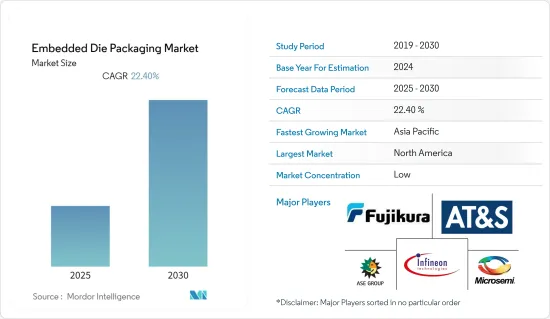
嵌入式晶片封装市场预计在预测期间内复合年增长率为 22.4%

主要亮点
- 随着产品变得更小、更丰富,设备小型化推动市场从生物医学应用到化学微反应器和感测器,微机械加工和奈米技术将在组件的小型化中发挥越来越重要的作用。例如,蓝牙无线 LAN 模组在当今的高密度行动装置中需要最小的电路基板空间。
- 电气和热性能的改进正在推动市场发展。在电源管理和行动无线应用中,嵌入式技术因其薄型和卓越的热性能而被视为组装製造的替代方案。嵌入式晶粒的热性能比铜夹的 PQFN 提高约 17%。对于电动车,我们还开发了一种用于功率元件的新型可扩展先进封装,该封装使用嵌入式晶粒和线路重布(RDL) 技术来提高电气和热性能。
- 此外,由于其在高频下优异的电气性能,该技术也被认为是新兴 IT 和通讯应用的一项有前途的技术。有助于在通讯应用中部署该技术的各种好处包括改进电子电路的功能和效率、改进功率和讯号电感、提高可靠性以及增加讯号密度。
- 嵌入式晶粒技术难以测试、检查和重工,是市场成长的挑战。当特征(线条和空间)变得小于 2μm 时,就很难看到缺陷。此外,根据应用的不同,在通孔内寻找碎片也成为一个问题。
- 自COVID-19爆发以来,电子产业受到重创,供应链和生产设施受到严重影响。 2 月至 3 月,中国大陆和台湾地区停产,影响了全球各OEM。
嵌入式晶片封装市场趋势
软基板晶粒可望占据较大市场占有率
- 随着技术的进步,印刷基板的产品销售量不断增加,随着柔性基板越来越多地应用于各种可穿戴和物联网设备,未来销售量预计将进一步增加。
- 伸缩性电子装置 (SC) 目前已在商业性销售,并有多种形状和形式。该技术主要使用称为柔性基板的标准印刷电路基板,并使用液体射出成型技术来形成包含合成橡胶体的可拉伸电子电路,从而产生坚固可靠的产品。例如,在军事应用中,灵活、轻巧的衝击感测器可以嵌入製服和装甲中,以储存有关战斗中受伤的资讯并提供更好的情报。
- 柔性混合电子(FHE)被认为是电子电路製造的新方法,旨在结合传统电子和印刷电子的优势。 IC 采用微影术製造并作为裸晶安装。
- 由于柔性电路在各种小型电子设备中的实现,其嵌入活动往往很高。例如,2019 年 9 月,IDEMIA 和 Zwipe 合作开发了生物识别付款卡解决方案,其中安全元件和微控制器等全部整合到安装在柔性印刷电路基板的单一晶片中,计画透过零件数量相对较少。
- 此外,运动应用和医疗应用的自主系统主要受益于小尺寸,因为精细的结构提供了最大的灵活性和舒适度。透过将现成的 IC 整合到柔性电路基板(FCB) 中,可以缩小整个系统的尺寸。使用液晶聚合物 (LCP) 作为感测器基板在医疗产品中非常常见。用于医疗应用的微型智慧感测器模组可以使用传统的柔性电路薄膜和标准组装製程和设备,由 LCP基板製造。
预计北美将占据较大市场占有率
- 美国也是半导体封装创新的领导者,在 19 个州拥有 80 家晶圆厂,引进嵌入式晶粒小型化等新技术。另外,跨国公司对美国的投资正在提振市场。
- 例如,英特尔正在利用英特尔的 3D系统级封装技术,透过嵌入式晶片互连桥 (EMIB) 来支援下一代平台。业界将这种应用称为2.5D封装整合。 EMIB(嵌入式多晶片互连桥)使用具有多个布线层的非常小的桥晶片,而不是使用其他 2.5D 方法中常见的大型硅内插器。此桥晶粒是我们基板製造过程的一部分。
- 除此之外,美国还有一些世界领先的汽车製造商投资电动车领域。嵌入式系统透过主动车距控制巡航系统等驾驶辅助功能提高了驾驶舒适度。要达到显着的节能,还需要采用分散式嵌入式控制方法来控制整个车辆的电源管理。这将增加对嵌入式晶粒技术的需求。
嵌入式晶片封装产业概述
由于汽车、工业和家用电子电器最终用户数量不断增加,嵌入式晶片封装市场变得支离破碎。市场上的现有参与企业正试图透过适应 5G通讯、高性能资料中心和小型电子产品等新技术来保持竞争力。主要参与企业包括 Microsemi Corporation 和 Fujikura Ltd.。近期市场发展趋势如下。
- 2020 年 10 月 -美国国防部将异质整合原型 (SHIP) 计画第二阶段授予英特尔联邦有限责任公司。 SHIP计画让美国政府可以利用英特尔在亚利桑那州和奥勒冈州的尖端半导体封装能力,利用英特尔每年数百亿美元的研发和製造投资所创造的能力。该计划将由海军水面作战中心起重机分部执行,并由国家安全技术加速器管理。
- 2019 年 9 月 - 基于 FPGA 的硬体加速器元件和高效能 eFPGA IP 的领先供应商 Achronix 半导体公司已加入台积电 IP 联盟计划,该计划是台积电开放创新平台 (OIP) 的关键组成部分。在台积电开放创新平台生态系统论坛的展位上,Achronix 展示了其 Speedcore IP 如何针对每个客户应用进行独特的调整和最佳化。
其他好处
- Excel 格式的市场预测 (ME) 表
- 3 个月分析师支持
目录
第一章简介
- 研究假设和市场定义
- 调查范围
第二章调查方法
第三章执行摘要
第四章市场动态
- 市场概况
- 市场驱动因素
- 设备小型化的进展
- 改善电气和热性能
- 市场限制因素
- 检查、测试和返工困难
- 价值链分析
- 产业吸引力-波特五力分析
- 供应商的议价能力
- 买家/消费者的议价能力
- 新进入者的威胁
- 替代品的威胁
- 竞争公司之间敌对关係的强度
- COVID-19 对市场的影响
第五章技术概况
- PCB小型化
- 先进的嵌入式主动系统集成
第六章 市场细分
- 平台
- 硬基板晶粒
- 软体基板晶粒
- IC封装基板
- 最终用户
- 消费性电子产品
- 资讯科技/通讯
- 车
- 医疗保健
- 其他的
- 地区
- 美洲
- 欧洲/中东/非洲
- 亚太地区
第七章 竞争格局
- 公司简介
- Microsemi Corporation
- Fujikura Ltd
- Infineon Technologies AG
- ASE Group
- AT&S Company
- Schweizer Electronic AG
- Intel Corporation
- Taiwan Semiconductor Manufacturing Company
- Shinko Electric Industries Co. Ltd
- Amkor Technology
- TDK Corporation
第八章投资分析
第九章 市场机会及未来趋势
The Embedded Die Packaging Market is expected to register a CAGR of 22.4% during the forecast period.

Key Highlights
- Growing miniaturization of devices is driving the market as products are becoming increasingly smaller and embed more functionality. Micromachining and nanotechnology play an increasingly important role in the miniaturization of components ranging from biomedical applications to chemical microreactors and sensors. For instance, Bluetooth wifi modules requires minimal circuit board area on today's high-density mobile devices.
- Improved electrical & thermal performance is driving the market. For power management and mobile-wireless application the embedded technology has been evaluated to replace assembles fabrication by not only thinner thickness but due to superior thermal performance. The thermal performance of embedded die is better than PQFN with copper clip about 17%. Also a new and expandable advanced package for power devices is developed using embedded dies and redistribution layer (RDL) technology for electric car to improve the electric and thermal performance.
- Further, owing to its excellent electrical performance at high frequencies, the technology is also being perceived as a promising technology for emerging telecommunication applications. Various advantages that aid the deployment of the technology in telecommunication applications include increased functionality and efficiency of the electronic circuits, power and signal inductance, improved reliability, and higher signal density.
- Difficulty to test, inspect and rework, the embedded die technology challenges the market to grow. As features (lines and spaces) shrink to 2µm and below, it becomes more difficult to see defects. In addition, finding debris in via holes becomes a concern in some applications.
- Since the outbreak of COVID-19, the electronics industry has been hit severely, with a significant influence on its supply chain and production facilities. The production came to a stand still in China and Taiwan during February and March, which influenced various OEMs across the world.
Embedded Die Packaging Market Trends
Die in Flexible Board Expected to Hold Significant Market Share
- With the increased advancement in technology, the product sale value of the printed circuit board is increasing and with the increased adoption of the flexible board in various wearable and IoT devices, the sales are expected to grow higher in future.
- Stretchable Electronics (SC) is so far commercial and comes in many shapes and forms. The technology uses standard printed circuit board, mainly flexible board, where liquid injection molding techniques involve elastomer embedded stretchable electronic circuit, which achieves a robust and reliable product. For instance, in military usage, uniforms and armors can have embedded, flexible, lightweight impact sensors that could store and provide better information of the injury sustained during combat.
- Flexible hybrid electronics (FHE), which is considered as a novel approach to electronic circuit manufacturing, aims to combine the best of conventional and printed electronics. Additional components and as many as conductive interconnects are possible to be printed onto a flexible substrate, whereas the IC is produced using photolithography and then mounted, as a bare die.
- The embedding activity of flexible circuits are in high trend for their implementation in various miniature electronic devices. For instance, in September 2019, IDEMIA and Zwipe collaborated for a biometric payment card solution, where the solution is planned to be distinguished by its relatively small number of components, with things, like the Secure Element and the microcontroller, all embedded in a single chip mounted on a flexible printed circuit board.
- Further, autonomous systems for sports applications and healthcare mainly benefit from a small form factor, as minute structures result in maximal flexibility and comfort. The embedding of a commercially available IC in a flexible circuit board (FCB) can reduce the overall size of a system. The usage of liquid crystal polymer (LCP) as base material for sensors are highly used in medical products. Miniaturized smart sensor modules for medical applications can be fabricated from LCP substrates using conventional flex circuit thin film and standard assembly processes and equipment.
North America Expected to Hold Significant Market Share
- Countries in the region, such as United States assist the world in manufacturing, designing, and researching related to the semiconductor industry and United States is also the frontrunner in semiconductor packaging innovation having 80 wafer fabrication plants spread across 19 states where new technologies is being implemented such as miniaturization through embedded die etc. Apart from this, investments in this country by global players are setting to fuel the market.
- For instance, Intel is enabling Next-Generation Platforms using Intel's 3D System-in-package technology through Embedded Multi-die Interconnect Bridge (EMIB) , an elegant and cost-effective approach to in-package high density interconnect of heterogeneous chips. The industry refers to this application as 2.5D package integration. Instead of using a large silicon interposer typically found in other 2.5D approaches, Embedded Multi-die Interconnect Bridge (EMIB) uses a very small bridge die, with multiple routing layers. This bridge die is embedded as part of our substrate fabrication process.
- Apart from this, the United States is home to some of the major automotive players in the world, which are investing in the electric car segment. The embedded systems increases the driving comfort with driver assistance functions like adaptive cruise control. Also to achieve significant energy savings, a distributed embedded control approach becomes necessary to control the power management of the entire vehicle. This is set to increase the demand for embedded die technology.
Embedded Die Packaging Industry Overview
The embedded die packaging market is fragmented due to the growing number of end-users in automotive, industrial, and consumer electronics. The existing players in the market are striving to maintain a competitive edge by catering to newer technologies, such as 5G telecommunication, high-performance data centers, compact electronic devices, etc. Key players are Microsemi Corporation, Fujikura Ltd, etc. Recent developments in the market are -
- October 2020 - The U.S. Department of Defence awarded Intel Federal LLC the second phase of its Heterogeneous Integration Prototype (SHIP) program. The SHIP program enables the US government to access Intel's state-of-the-art semiconductor packaging capabilities in Arizona and Oregon and take advantage of capabilities created by Intel's tens of billions of dollars of annual R&D and manufacturing investment. The project is executed by the Naval Surface Warfare Centre, Crane Division, and administered by the National Security Technology Accelerator.
- Sep 2019 - Achronix Semiconductor Corporation, a leading supplier in FPGA-based hardware accelerator devices and high-performance eFPGA IP, joined the TSMC IP Alliance Program, a key component of TSMC Open Innovation Platform (OIP). Achronix demonstrated how its Speedcore IP is uniquely sized and optimized for each customer's application in its booth at TSMC Open Innovation Platform Ecosystem Forum.
Additional Benefits:
- The market estimate (ME) sheet in Excel format
- 3 months of analyst support
TABLE OF CONTENTS
1 INTRODUCTION
- 1.1 Study Assumptions and Market Definition
- 1.2 Scope of the Study
2 RESEARCH METHODOLOGY
3 EXECUTIVE SUMMARY
4 MARKET DYNAMICS
- 4.1 Market Overview
- 4.2 Market Drivers
- 4.2.1 Growing Miniaturization of Devices
- 4.2.2 Improved Electrical and Thermal Performance
- 4.3 Market Restraints
- 4.3.1 Difficulty to Inspect, Test and Rework
- 4.4 Industry Value Chain Analysis
- 4.5 Industry Attractiveness - Porter's Five Forces Analysis
- 4.5.1 Bargaining Power of Suppliers
- 4.5.2 Bargaining Power of Buyers/Consumers
- 4.5.3 Threat of New Entrants
- 4.5.4 Threat of Substitute Products
- 4.5.5 Intensity of Competitive Rivalry
- 4.6 Impact of COVID-19 on the Market
5 TECHNOLOGY SNAPSHOT
- 5.1 PCB Miniaturization
- 5.2 Advanced Embedded Active System Integration
6 MARKET SEGMENTATION
- 6.1 Platform
- 6.1.1 Die in Rigid Board
- 6.1.2 Die in Flexible Board
- 6.1.3 IC Package Substrate
- 6.2 End User
- 6.2.1 Consumer Electronics
- 6.2.2 IT and Telecommunications
- 6.2.3 Automotive
- 6.2.4 Healthcare
- 6.2.5 Other End Users
- 6.3 Geography
- 6.3.1 Americas
- 6.3.2 Europe and MEA
- 6.3.3 Asia-Pacific
7 COMPETITIVE LANDSCAPE
- 7.1 Company Profiles
- 7.1.1 Microsemi Corporation
- 7.1.2 Fujikura Ltd
- 7.1.3 Infineon Technologies AG
- 7.1.4 ASE Group
- 7.1.5 AT&S Company
- 7.1.6 Schweizer Electronic AG
- 7.1.7 Intel Corporation
- 7.1.8 Taiwan Semiconductor Manufacturing Company
- 7.1.9 Shinko Electric Industries Co. Ltd
- 7.1.10 Amkor Technology
- 7.1.11 TDK Corporation


