


 |
市场调查报告书
商品编码
1631588
亚太地区晶片贴装设备:市场占有率分析、产业趋势、成长预测(2025-2030)APAC Die Attach Equipment - Market Share Analysis, Industry Trends & Statistics, Growth Forecasts (2025 - 2030) |
||||||
价格
※ 本网页内容可能与最新版本有所差异。详细情况请与我们联繫。
简介目录
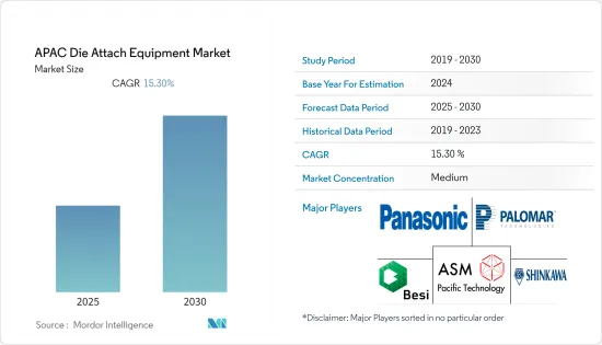
亚太晶片贴装设备市场预计在预测期内复合年增长率为 15.3%
主要亮点
- 市场供应商下一轮投资的重点将是为小型且高度复杂的 5G 智慧型手机开发晶粒键合和封装解决方案。 5G 是面向未来创新的统一连接平台,可实现持续安全的云端存取以及显着更快的资料和视讯传输。
- 用户对 5G 功能的采用将扩大行动宽频活动,并加速人工智慧在万物互联的应用。同样,用于行动互联网、计算、5G 和汽车最终用户的基板和晶圆层次电子构装製程引领了半导体产业记忆体和逻辑资本支出的復苏。
- 该公司已共用在中长期内增加资本投资,以扩大半导体和 FPD 应用。另一方面,在半导体组装设备方面,FOWLP/PLP、μLED等高速高精度接合设备的积极开发受到关注。
- BESI共用了针对新数位社会的新组装技术的投资计划,包括 FOWLP、TCB、TSV、超薄晶粒、混合键合、大面积、晶圆级成型、太阳能和 3D 锂离子电池电镀。我们的晶片贴装设备系列包括单晶片、多晶片、多模组、覆晶、TCB、FOWLP、混合晶粒键合系统和晶片分类系统。
- 然而,令人担忧的是,由于 COVID-19 全球传播的影响,未来仍存在不确定性。由于 COVID-19 爆发,整个亚太地区的营运关闭和生产暂停对半导体生产和消费产生了重大影响。由于大多数 IDS 和代工厂都位于该地区,因此停产的影响导致资本设备支出减少。这可能会对市场研究产生影响,预计復苏将放缓至 2021 年。
亚太晶片贴装设备市场趋势
CIS预计将大幅成长
- CMOS 影像感测器为智慧型手机和其他产品提供了相机功能,但随着对更小尺寸的需求增加,晶圆厂出现了製造问题。
- 从3G到4G,再到现在的5G,资料效能变得宽频化,对更高品质相机的需求也不断增加。由于需要更高的像素数和分辨率,这一趋势推动了 CMOS 影像感测器的堆迭技术的发展。除了这些趋势之外,生物辨识 ID、3D 感测和增强型人类视觉应用领域也正在促进该领域的成长。
- 客户对更大更好相机的需求正在推动晶粒尺寸更大的感测器的兴起。除了像素缩放之外,CMOS 影像感测器正在经历晶粒堆迭等技术创新。该市场的供应商使用各种互连技术,例如硅穿孔电极(TSV)、混合键合和像素到像素键合。
- 例如,在混合键合中,晶粒透过铜对铜互连进行连接。为此,在晶圆厂中加工两片晶圆。一种是逻辑晶圆,另一种是像素阵列晶圆。使用电介质对电介质键结然后使用金属对金属键合将两个晶片连接起来。
- Xperi 专有的混合结 DBI 技术大量用于三星行动电话的 CMOS 影像感测器的生产。这项用于 CMOS 影像感测器的技术有助于在室温下实现 Cu-Cu 永久键结、低温退火(~300°C)以及无外部压力的键结製程(电介质/金属)。
- 在此之前,直接键合技术在实现由 Xperifor主导的多代变体的像素缩放(背照式)BSI 和堆迭 BSI 方面发挥了可行的作用超过 15 年。
LED主导市场占有率
- 晶片黏接材料对于中、高和高功率LED 的性能和可靠性起着至关重要的作用。随着 LED 渗透率的提高,对晶片贴装设备的需求不断增加。针对特定晶片结构和应用选择适当的晶片贴装材料取决于多种考虑因素,包括封装製程(吞吐量和产量比率)、性能(热输出和光输出)、可靠性(流明维持率)和成本。共晶金锡、银填充环氧树脂、焊料、硅胶和烧结材料已用于 LED 晶片贴装。
- SFE提供环氧胶黏合方法,可提供0.2秒/週期的LED环氧固晶机索引时间(90%操作率),晶片尺寸250*250标准,并透过两个相机识别导线架。其软体功能包括自动安装水平仪和拾取水平仪教学功能。
- 此外,导电黏合剂(主要是银填充环氧树脂)构成了 LED 热晶片黏合材料的最大类别(按数量计算)。它们与现有的后端封装设备相容,并提供有吸引力的成本/性能平衡(通常高达 50W/mK 热量,具有二次回流焊接相容性)。由于它附着在裸硅上,因此它是无后端金属化晶片(例如硅基氮化镓)的最优选材料。
- 此外,儘管LED市场竞争者众多,ASM是该市场的主要参与企业之一,其LED环氧树脂高速固晶机AD830在LED市场中占据主导地位。快速、可靠且准确,晶粒贴装精度为 +/-1 mil、+/-3 度,小型晶片(如 10 mil x 10 mil)的週期时间为 180 ms,相当于 18,000 UPH。它配备了键合后检查系统,可在预先定义的放置范围内监控键合单元。
亚太地区晶片贴装设备产业概况
亚太晶片贴装设备市场竞争适中,众多公司占较小的市场占有率。公司不断创新并结成策略伙伴关係以维持市场占有率。
- 2022 年 4 月 - 电气革命工业化中心 (DER-IC) 东北部接受来自领先的工具和材料技术分销商 Inseto 的设备,以增强其电力电子、机器和驱动器 (PEMD) 能力。英国安装的第一台微冲床是 AMX P100 烧结机,它是所提供设备的一部分,能够生产高度可靠、高功率的模组。
- 2022年6月-West Bond开发了新的7KF键合机系列。这家知名公司为微电子封装产业设计和製造一系列焊线机、晶粒装机、引线拉伸试验机、剪切试验机、超音波元件和配件。这款卓越的工具专为处理射频、微波、半导体、混合动力和医疗设备领域的困难黏合应用而设计。
其他好处
- Excel 格式的市场预测 (ME) 表
- 3 个月分析师支持
目录
第一章简介
- 研究假设和市场定义
- 调查范围
第二章调查方法
第三章执行摘要
第四章市场动态
- 市场概况
- 产业吸引力-波特五力分析
- 供应商的议价能力
- 买方议价能力
- 新进入者的威胁
- 替代品的威胁
- 竞争公司之间的敌对关係
- 产业价值链分析
- COVID-19 对市场的影响
第五章 市场促进因素
- 对 AuSn 共晶晶片贴装技术的需求不断增长
- 对分立功率元件的需求
第六章 市场问题
- 加工和寿命期间的尺寸变化和机械不平衡
第七章 市场区隔
- 接合技术
- 固晶机
- 环氧树脂/黏合剂(糊剂/薄膜)
- 共晶
- 焊接
- 烧结
- 覆晶键合机
- 取货/回流焊接焊接
- 热压缩 (TCB)
- 热超音波黏合
- 混合键合
- 固晶机
- 目的
- 记忆
- LED
- 逻辑
- CMOS影像感测器
- 光电子/光电
- 分离式功率元件
- 微机电系统和感测器
- 堆迭记忆体和射频
- 国家名称
- 台湾
- 中国
- 日本
- 韩国
- 东南亚
第八章 竞争格局
- 公司简介
- Palomar Technologies, Inc.
- Shinkawa Ltd
- Panasonic Corporation
- ASM Pacific Technology Limited
- Be Semiconductor Industries NV(Besi)
- Shibaura Mechatronics Corporation
- ficonTEC Trading Ltd(ficonTEC Service GmbH)
- Fasford Technology Co Ltd.
- Dongguan Hoson Electronic Technology Ltd
- For Technos Co., Ltd.
- Shenzhen Xinyichang Technology Co., Ltd.(Hoson)
第 9 章 供应商市场占有率分析 ~ 2021
第十章投资分析
第十一章投资分析市场的未来
简介目录
Product Code: 71756
The APAC Die Attach Equipment Market is expected to register a CAGR of 15.3% during the forecast period.
Key Highlights
- A significant focus for the next investment round by market vendors is developing die bonding and packaging solutions for smaller and highly complex 5G compatible smartphones. 5G is a unifying connectivity platform for future innovation, enabling continuous secure cloud access at significantly higher data and video transmission speeds.
- User adoption of 5G capabilities expands mobile broadband activities and accelerates artificial intelligence usage for the Internet of Everything. Likewise, the substrate and wafer-level packaging processes for mobile internet, computing, 5G, and automotive end-user applications drove the semiconductor industry to see a recovery in capital investment for memories and logic.
- The company has shared plans for a medium-to-long-term increase in capital investment towards expanded semiconductor and FPD applications. Whereas, as per Shibaura, active development of high-speed, high-precision bonding equipment for FOWLP / PLP and μLED is being looked out for in semiconductor assembly equipment.
- BESI has shared plans to invest in new assembly technologies such as FOWLP, TCB, TSV, ultra-thin dies, hybrid bonding, large area, wafer level molding, solar, and 3D-lithium-ion battery plating for the new digital society. Its lineup under Die attach equipment includes a single chip, multi-chip, multi-module, flip chip, TCB, FOWLP, hybrid die bonding systems, and die sorting systems.
- However, one source of concern is the continuing uncertain outlook due to the impact of the global spread of COVID-19. Lockdowns and production halts across Asia-pacific due to the COVID-19 outbreak had significantly impacted the production and consumption of semiconductors. With the majority of the IDS and foundries located in the region, the impact of shutdowns has led to reduced spending on capital investments. This is likely to impact the market studied, with a slowed recovery expected across 2021.
APAC Die Attach Equipment Market Trends
CIS is expected to witness significant growth
- CMOS image sensors have been offering camera functions in smartphones and other products, and as the scaling demand grows, the related manufacturing issues in the fab arise.
- The higher-bandwidth data performance progressed from 3G to 4G, and currently, to 5G, the demand for higher quality cameras has grown. This trend has propelled the CMOS image sensor stacking techniques based on the need for higher pixel counts and better resolution. Beyond these trends, the areas of biometric ID, 3D sensing, and enhanced human vision applications have augmented segment growth.
- Customer demand for bigger and better cameras results in more sensors with bigger die sizes. Besides pixel scaling, CMOS image sensors are undergoing other innovations like die stacking. Vendors in the market studied are also using different interconnect technologies, such as through-silicon vias (TSVs), hybrid bonding, and pixel-to-pixel for the same.
- In hybrid bonding, for instance, the dies are connected using copper-to-copper interconnects. For this, two wafers are processed in a fab. One is the logic wafer, while the other is the pixel array wafer. The two wafers are joined using a dielectric-to-dielectric bond, followed by a metal-to-metal connection.
- Hybrid bonding DBI technologies, Xperi'sproprietary technology, are being significantly used by Samsung towards CMOS image sensor fabrication for its phones. This technology for CMOS Image Sensors facilitates room temperature Cu-Cu permanent bonding, low-temperature annealing (around 300°C) & no external pressure bonding process (dielectric/metal).
- Prior to this, direct bond technology has thus played an enabling role in the realization of pixel scaling (backside illumination) BSI and stacked BSI with multiple generational variations led by Xperifor over 15 years.
LED to dominate market share
- Die attach material represents a key role in the performance and reliability of mid, high, and super-high power LEDs. The demand for die-attach equipment is increasing with an increasing LED penetration rate. The selection of suitable die-attach material for a particular chip structure and application depends on various considerations, which include the packaging process (throughput and yield), performance (thermal dissipation output and light output), reliability (lumen maintenance), and cost. Eutectic gold-tin, silver-filled epoxies, solder, silicones, and sintered materials have all been used for LED die attach.
- SFE provides an Epoxy Adhesive bonding method where its LED Epoxy Die Bonder machine features an index time of 0.2 Sec /Cycle (90 Percent Rate of Operation) with a chip size of 250 * 250 standards, providing lead frame recognition through 2 Cameras. Its software function provides auto mount level & pick up level teaching functions.
- Further, conductive adhesives (mostly silver-filled epoxies) constitute the largest class of thermal die-attach materials (by unit number) for LEDs. They are compatible with existing back-end packaging equipment and provide an attractive cost/performance balance (typically up to 50 W/mK thermals with secondary reflow compatibility). As they stick to bare silicon, they are the most preferred material for dies without back-end metallization like GaN on silicon.
- Further, in the LED market, there are a lot of rival competitors, and ASM is one of the prominent players in this market; its LED Epoxy High speed die bonder AD830 dominates in the LED market. It is fast, reliable, and accurate with die placement accuracy of +/-1 mil and +/-3 degree, cycle time for a small chip like 10mil x 10mil is 180 ms, which is an equivalent UPH of 18,000. It is equipped with a Post bond inspection system that monitors the bonded unit at the pre-set placement range.
APAC Die Attach Equipment Industry Overview
The APAC Die attach equipment market is moderately competitive, with a large number of players having a small market share. The companies keep innovating and entering into strategic partnerships to maintain their market share.
- April 2022 - Driving the Electric Revolution Industrialization Centre (DER-IC) North East has received equipment from Inseto, a top technical distributor of tools and materials, to improve its power electronics, machines, and drives (PEMD) capabilities. The first micro-punch machine to be installed in the UK is an AMX P100 sinter press, which is part of the equipment provided and will allow the production of high-reliability, high-power modules.
- June 2022 - The new 7KF Bonder Series has been developed by West Bond. This well-known company designs and manufactures a line of wire bonding and die-to-attach machines, wire pull and shear test equipment, ultrasonic components, and accessories for the microelectronics packaging industry. This excellent tool is made to handle the difficult bonding applications found in the RF, microwave, semiconductor, hybrid, and medical device fields.
Additional Benefits:
- The market estimate (ME) sheet in Excel format
- 3 months of analyst support
TABLE OF CONTENTS
1 INTRODUCTION
- 1.1 Study Assumptions and Market Definition
- 1.2 Scope of the Study
2 RESEARCH METHODOLOGY
3 EXECUTIVE SUMMARY
4 MARKET DYNAMICS
- 4.1 Market Overview
- 4.2 Industry Attractiveness - Porter's Five Forces Analysis
- 4.2.1 Bargaining Power of Suppliers
- 4.2.2 Bargaining Power of Buyers
- 4.2.3 Threat of New Entrants
- 4.2.4 Threat of Substitutes
- 4.2.5 Intensity of Competitive Rivalry
- 4.3 Industry Value Chain Analysis
- 4.4 Impact of Covid-19 on the market
5 Market Drivers
- 5.1 Growing Demand of AuSn Eutectic Die-Attach Technology
- 5.2 Demand of Discrete Power Devices
6 Market Challenges
- 6.1 Dimensional Changes During Processing and Service Life and Mechanical Unbalance
7 MARKET SEGMENTATION
- 7.1 By Bonding Technique
- 7.1.1 Die Bonder
- 7.1.1.1 Epoxy/Adhesive (paste/film)
- 7.1.1.2 Eutectic
- 7.1.1.3 Solder
- 7.1.1.4 Sintering
- 7.1.2 Flip Chip Bonder
- 7.1.2.1 Pick and Place / reflow soldering
- 7.1.2.2 Thermocompresion (TCB)
- 7.1.2.3 Thermosonic Bonding
- 7.1.2.4 Hybrid Bonding
- 7.1.1 Die Bonder
- 7.2 Application
- 7.2.1 Memory
- 7.2.2 LED
- 7.2.3 Logic
- 7.2.4 CMOS Image Sensor
- 7.2.5 Optoelectronics / Photonics
- 7.2.6 Discrete Power Devices
- 7.2.7 MEMS & Sensors
- 7.2.8 Stacked Memory & RF
- 7.3 Country
- 7.3.1 Taiwan
- 7.3.2 China
- 7.3.3 Japan
- 7.3.4 Korea
- 7.3.5 Southeast Asia
8 COMPETITIVE LANDSCAPE
- 8.1 Company Profiles
- 8.1.1 Palomar Technologies, Inc.
- 8.1.2 Shinkawa Ltd
- 8.1.3 Panasonic Corporation
- 8.1.4 ASM Pacific Technology Limited
- 8.1.5 Be Semiconductor Industries NV (Besi)
- 8.1.6 Shibaura Mechatronics Corporation
- 8.1.7 ficonTEC Trading Ltd (ficonTEC Service GmbH)
- 8.1.8 Fasford Technology Co Ltd.
- 8.1.9 Dongguan Hoson Electronic Technology Ltd
- 8.1.10 For Technos Co., Ltd.
- 8.1.11 Shenzhen Xinyichang Technology Co., Ltd. (Hoson)
9 VENDOR MARKET SHARE ANALYSIS - 2021
10 INVESTMENT ANALYSIS
11 FUTURE OF THE MARKET
02-2729-4219
+886-2-2729-4219
 自动银烧结晶片贴装机市场报告:趋势、预测及竞争分析(至2031年)
 2025-2033 年晶片黏接机市场报告(按类型、技术、应用和地区)
 晶片贴装设备:市场占有率分析、产业趋势与统计、成长预测(2025-2030 年)