


 |
市场调查报告书
商品编码
1644780
3D IC封装:市场占有率分析、产业趋势与统计、成长预测(2025-2030 年)3D IC Packaging - Market Share Analysis, Industry Trends & Statistics, Growth Forecasts (2025 - 2030) |
||||||
价格
※ 本网页内容可能与最新版本有所差异。详细情况请与我们联繫。
简介目录
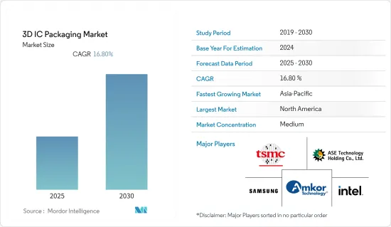
预测期内 3D IC封装市场预计复合年增长率为 16.8%
关键亮点
- 在不断发展的微电子和半导体产业中,垂直堆迭积体电路(IC)的趋势正在不断发展,并成为一种可行的解决方案,可提供高性能、功能性和低功耗,以满足电子设备的要求。连网型设备、平板电脑、智慧型手机和其他电子产品正在推动对先进架构的快速需求,以提高能源效率、效能,并且不仅仅是发送简讯和通话。这些因素预计将推动 3D IC封装市场的成长。
- 由于半导体应用的不断增加,CMOS 扩展放缓和成本上升迫使产业转向先进的 IC 封装。 3D增材技术已成为满足机器学习、人工智慧和资料中心等应用效能要求的有利解决方案。因此,在预测期内,对高效能运算应用的不断增长的需求将推动 3D-TSV(硅通孔)市场的发展。
- 此外,电子设备的持续小型化也有望成为市场成长的驱动力。平板电脑、智慧型手机和游戏设备对先进架构的需求不断增长,以及感测器和 MEMS 中先进晶圆层次电子构装技术的使用激增,预计将在预测期内为 3D IC封装市场提供成长前景。根据WSTS预测,2021年半导体IC市场收益可望达4,630亿美元,2022年将成长10%以上,达到5,109.6亿美元。
- 新冠肺炎疫情为各行各业带来重大影响,同时也促进了全球先进医疗设备及器材的发展。各医疗设备製造公司宣布,疫情爆发后,将增加多种新仪器设备的产量。由于 3D IC封装在医疗产业的应用非常广泛,预计製造业倡议的增加将推动对 3D IC封装的需求。
- 然而,高昂的初始投资和半导体积体电路设计的日益复杂性预计会抑制市场的发展。
3D IC封装市场趋势
资讯科技和通讯产业可望强劲成长
- 3D IC封装是半导体製造和设计中的重要元素。从宏观层面来看,它影响性能、功率和成本;从微观层面来看,它直接影响每个晶片的基本功能。
- 5G 基础设施投资不断增加、资料中心和伺服器数量不断增加,再加上物联网连接和网路设备,这些都是推动 IT 和通讯领域 3D IC封装成长的因素。例如,包括 KT、LG Uplus 和 SK Telecom 在内的韩国行动电话营运商已同意在 2022 年投资总计 25.7 兆韩元,以支援全国的 5G 基础设施。追加投资将集中用于提升首尔等六个城市的5G品质。
- 资料中心的扩张为研究3D IC封装的供应商提供了成长机会。根据思科公司预测,2021年全球资料中心储存的巨量资料量将达到Exabyte,其中美国占了很大比例。到 2021 年,超大规模资料中心的数量将从 2015 年的 259 个增加到 700 个。
- 此外,物联网市场的发展和无线技术需求的激增(更小的占用空间和更高的效率是关键)预计将推动 3D IC封装市场的发展。根据爱立信预测,到 2027 年,广域物联网设备数量将从 2021 年的 21 亿增加到 52 亿。
预计亚太地区将出现显着成长
- 亚太地区是主要半导体晶片製造商和公司的所在地,例如台积电、中芯国际、联电和韩国三星。一家领先的台湾晶片代工厂正在与日本供应商合作,争夺关键的 3 奈米晶片市场的主导地位。例如,2021年2月,台积电宣布将在日本科学城筑波建立研发中心,与日本供应商合作开发3D IC封装材料。
- 另外,2021年5月,日本经济产业省及其下属机构日本产业技术综合研究所宣布,约20家日本公司将与台积电日本3D IC研发中心合作。
- 亚太地区也占据了 3D IC封装市场的很大份额,因为该地区拥有大量半导体製造业务,并且拥有三星电子、东芝公司、日月光集团和联华电子等主要市场参与企业。
- 亚太地区以其强大的汽车製造能力而闻名。此外,5G技术在汽车产业的不断商业化,为受调查市场中的供应商带来了新的收益来源。基于 5G NR 的 C-V2X 的出现有望为自动驾驶汽车提供独特的功能。这可能推动对更高水准的自主性和可预测性以及车辆内其他 ADAS 感测器技术的需求。
- 此外,该地区的市场参与企业正专注于下一代晶片技术,这可以透过 3D 封装工具开启新的可能性。例如,日本工具製造商 Disco 专注于 3D 晶片封装,其中涉及在薄的、几乎透明的硅晶片上堆迭积体电路。随着摩尔定律接近其物理极限,晶片製造商正在探索新的设计和材料来提高下一代硬体的性能。预计这些趋势将推动该地区的成长。
- 在目前的智慧型设备和互联世界环境下,客户要求下一代设备更紧凑、功能更多、性能更佳、功耗更低。这使得对于高性价比、高性能 IC 的需求日益增加。例如,STAR 的微电子实验室与领先的半导体公司合作开发具有成本效益的 3D 晶圆级积体电路封装解决方案。该公司已推出晶圆晶片联盟 II 和成本效益内插器联盟,以推进大批量生产的晶片封装解决方案。这个以产业为重点的联盟致力于解决晶圆层次电子构装中的关键挑战,以降低整体製造成本并加快下一代电子设备的上市时间。
3D IC封装产业概况
全球 3D IC封装市场因 Amkor Technology Inc.、ASE Group 和 Siliconware Precision Industries (SPIL) 等主要参与者的存在而呈现细分化。市场参与企业必须不断创新,提供先进、全面的产品。
- 2021 年 5 月:英特尔计划投资 35 亿美元升级其里奥兰乔工厂,将这个庞大的综合体(美国三大製造地之一)的员工数量增加 35% 以上。英特尔正在扩建其新墨西哥工厂,以利用其 Foberos 3D 封装技术生产新一代晶片。
其他福利
- Excel 格式的市场预测 (ME) 表
- 3 个月的分析师支持
目录
第 1 章 简介
- 研究假设和市场定义
- 研究范围
第二章调查方法
第三章执行摘要
第四章 市场洞察
- 市场概况
- 产业吸引力-波特五力分析
- 新进入者的威胁
- 购买者/消费者的议价能力
- 供应商的议价能力
- 替代品的威胁
- 竞争对手之间的竞争强度
- 价值链分析
- COVID-19 市场影响评估
第五章 市场动态
- 市场驱动因素
- 电子产品先进架构
- 电子设备小型化
- 市场问题/顾虑
- 半导体IC设计初期投入高,复杂度增加
第六章 市场细分
- 封装技术
- 3D 晶圆级晶片规模封装
- 3D TSV
- 最终用户产业
- 家用电子电器
- 航太和国防
- 医疗设备
- 通讯和电讯
- 车
- 其他的
- 地区
- 北美洲
- 欧洲
- 亚太地区
- 拉丁美洲
- 中东和非洲
第七章 竞争格局
- 公司简介
- Taiwan Semiconductor Manufacturing Company Limited
- Samsung Electronics Co., Ltd.
- ASE Group
- Amkor Technology
- Intel Corporation
- Siliconware Precision Industries Co. Ltd(SPIL)
- GlobalFoundries
- Invensas
- Powertech Technology Inc.
第八章投资分析
第九章:市场的未来
简介目录
Product Code: 91074
The 3D IC Packaging Market is expected to register a CAGR of 16.8% during the forecast period.
Key Highlights
- The growing microelectronics and semiconductor industry is developing a trend for vertically stacked integrated circuits (ICs), emerging as a viable solution for providing high performance, increased functionality, and reducing power consumption to fulfill electronic device requirements. The surging need for advanced architecture in electronic products such as connected devices, tablets, and smartphones to increase their energy efficiency and performance to do more than just texting and calling. Such factors are expected to bolster the growth of the 3D IC packaging market.
- As a result of the growing semiconductor applications, the slowdown in CMOS scaling and escalating costs have forced the industry to depend on packaging advancements for ICs. 3D stacking technologies have emerged as lucrative solutions that meet the required performance of applications such as machine learning, AI, and data centers. Therefore, the growing need for high-performance computing applications drives the 3D-TSV (Through Silicon Via) market over the forecast period.
- The increasing miniaturization of electronics devices is also anticipated to drive market growth. Growing demand for advanced architecture in tablets, smartphones, and gaming devices, along with surging usage of advanced wafer-level packaging technologies in sensors and MEMS, is expected to provide growth prospects for the 3D IC packaging market during the forecast period. According to WSTS, the IC market for semiconductors reached USD 463 billion in revenue in 2021 and is expected to grow by over 10% to USD 510.96 billion in 2022.
- The COVID-19 pandemic has significantly impacted various industries and has simultaneously propelled the development of advanced medical equipment and devices across the globe. Various medical equipment manufacturing companies announced to increase in the production of several new equipment and devices post the pandemic outbreak. As the applications of 3D IC packaging are numerous within the medical and healthcare industry, the increased manufacturing initiatives are expected to boost the demand for 3D IC packaging.
- However, the high Initial Investment and Increasing Complexity of Semiconductor IC Designs are expected to restrain the evolution of the market.
3D IC Packaging Market Trends
IT & Telecommunication is Expected to Witness Significant Growth
- 3D IC Packaging is an essential part of semiconductor manufacturing and design. It directly affects performance, power, and cost on a macro level and the basic functionality of all chips on a micro level.
- The increasing investment in 5G infrastructure and the growing number of data center servers coupled with IoT connections and networking devices are the factors propelling the growth of 3D IC packaging in the IT and telecommunication sector. For instance, mobile operators in Korea such as KT, LG Uplus, and SK Telecom agreed to invest a total of KRW 25.7 trillion through 2022 to support 5G infrastructure across the country. The additional investment is focused on enhancing the 5G quality in Seoul and six other cities.
- The expansion of data centers provides a growth opportunity for the vendors in the 3D IC packaging studied. According to Cisco Systems, the amount of big data in data center storage global is anticipated to reach 403 exabytes in 2021, with a significant share in the US. Hyperscale data centers reached 700 in 2021, compared to 259 in 2015.
- Moreover, the growing IoT market and surging demand for wireless technologies, wherein reduced footprint and enhanced efficiency are critical, are expected to develop the market for 3D IC packaging. According to Ericson, wide-area IoT devices will reach 5.2 billion by 2027 from 2.1 billion in 2021.
Asia-Pacific is Expected to Witness Significant Growth Rate
- Asia Pacific is home to some of the biggest semiconductor chip manufacturers and companies like TSMC, SMIC, UMC, and South Korea's Samsung. Taiwan's leading chip foundry is teaming up with Japanese suppliers in the race to lead the crucial 3-nanometer chip market. For instance, in February 2021, TSMC announced that the company plans to establish an R&D center in Japan's science city of Tsukuba to develop 3D IC packaging materials in cooperation with its Japanese suppliers.
- Also, in May 2021, Japan's Ministry of Economy, Trade, and Industry and its subsidiary, the National Institute of Advanced Industrial Science and Technology, announced that approximately 20 Japanese companies would work with TSMC Japan's 3D IC R&D Center.
- The Asia Pacific region also holds a significant share in the 3D IC packaging market due to a considerable number of semiconductor manufacturing operations happening in the region, along with the presence of major market players such as Samsung Electronics Co., Ltd., Toshiba Corp, ASE Group, and United Microelectronics Corp. among others.
- The Asia Pacific region is known for its robust Automotive manufacturing capabilities. Moreover, the growing commercialization of 5G technology in the automotive industry will provide a new revenue stream for the vendors operating in the studied market. The advent of 5G NR-based C-V2X is anticipated to offer unique capabilities for the autonomous vehicle. Thus, it can propel the need for higher levels of autonomy and predictability and other ADAS sensor technologies in the vehicle.
- Additionally, market players in the region are forcing on Next-gen chip technology, which could unlock new potential with 3D packaging tools. For instance, Japanese tool-making company Disco focuses on 3D chip packaging by stacking integrated circuits on silicon wafers of near-transparent thinness. As Moore's Law nears its physical limits, chipmakers seek new designs and materials to get better performance out of next-generation hardware. Such trends are expected to propel growth in the region.
- In the current scenario of smart devices and the connected world, customers demand next-generation devices that are more compact, multi-functional, offer better performance, and consume less power. This has propelled the demand for cost-efficient and high-performance IC. For instance, STAR's Institute of Microelectronics has partnered with leading semiconductor companies to develop cost-effective 3D wafer-level integrated circuit packaging solutions. The company has launched chip-on-wafer consortium II and the cost-effective Interposer consortium to advance chip packaging solutions for high-volume manufacturing. The industry-focused consortium will address key challenges in wafer-level packaging to low overall manufacturing costs to accelerate time-to-market for next-generation electronics devices.
3D IC Packaging Industry Overview
The Global 3D IC Packaging Market is fragmented due to the presence of significant players such as Amkor Technology Inc., ASE Group, and Siliconware Precision Industries Co. Ltd (SPIL), among others. The market players must constantly innovate advanced and comprehensive products to stay relevant.
- In May 2021: Intel plans to invest USD 3.5 billion to upgrade its Rio Rancho plant and increase its headcount by more than 35% at the sprawling complex, one of its three largest US manufacturing hubs. It is expanding its New Mexico operations to manufacture new generations of chips based on its Foveros 3D packaging technology, which could aid the company's attempts to regain its leadership status in the semiconductor industry.
Additional Benefits:
- The market estimate (ME) sheet in Excel format
- 3 months of analyst support
TABLE OF CONTENTS
1 INTRODUCTION
- 1.1 Study Assumptions and Market Definition
- 1.2 Scope of the Study
2 RESEARCH METHODOLOGY
3 EXECUTIVE SUMMARY
4 MARKET INSIGHT
- 4.1 Market Overview
- 4.2 Industry Attractiveness - Porter's Five Forces Analysis
- 4.2.1 Threat of New Entrants
- 4.2.2 Bargaining Power of Buyers/Consumers
- 4.2.3 Bargaining Power of Suppliers
- 4.2.4 Threat of Substitute Products
- 4.2.5 Intensity of Competitive Rivalry
- 4.3 Value Chain Analysis
- 4.4 Assessment of the Impact of COVID-19 on the Market
5 MARKET DYNAMICS
- 5.1 Market Drivers
- 5.1.1 Growing Advanced Architecture in Electronic Products
- 5.1.2 Miniaturization of Electronics Devices
- 5.2 Market Challenges/Restrains
- 5.2.1 High Initial Investment and Increasing Complexity of Semiconductor IC Designs
6 MARKET SEGMENTATION
- 6.1 Packaging Technology
- 6.1.1 3D wafer-level chip-scale packaging
- 6.1.2 3D TSV
- 6.2 End-User Industry
- 6.2.1 Consumer electronics
- 6.2.2 Aerospace and Defense
- 6.2.3 Medical Devices
- 6.2.4 Communications and Telecom
- 6.2.5 Automotive
- 6.2.6 Others
- 6.3 Geography
- 6.3.1 North America
- 6.3.2 Europe
- 6.3.3 Asia-Pacific
- 6.3.4 Latin America
- 6.3.5 Middle-East and Africa
7 COMPETITIVE LANDSCAPE
- 7.1 Company Profiles
- 7.1.1 Taiwan Semiconductor Manufacturing Company Limited
- 7.1.2 Samsung Electronics Co., Ltd.
- 7.1.3 ASE Group
- 7.1.4 Amkor Technology
- 7.1.5 Intel Corporation
- 7.1.6 Siliconware Precision Industries Co. Ltd (SPIL)
- 7.1.7 GlobalFoundries
- 7.1.8 Invensas
- 7.1.9 Powertech Technology Inc.
8 INVESTMENT ANALYSIS
9 FUTURE OF THE MARKET
02-2729-4219
+886-2-2729-4219
 3D IC 和 2.5D IC封装市场分析及预测(至 2035 年):按类型、产品、服务、技术、组件、应用、材料类型、製程、最终用户和设备划分
 2026年全球携带式无线保真度(Wi-Fi)市场报告
 半导体封装和测试系统市场:按封装类型、测试类型、设备类型、封装材料和最终用途划分,全球预测,2026-2032年半导体封装和测试设备市场:按设备类型、封装技术、装置类型、工作模式和最终用户产业划分,全球预测,2026-2032年ePOP包装和测试市场按产品类型、材料、最终用途产业、测试类型和分销管道划分,全球预测,2026-2032年类比数位IC开发工具市场分析及预测(至2035年):按类型、产品类型、服务、技术、组件、应用、外形、装置、部署类型和最终用户划分2026年全球3D IC和2.5D IC封装市场报告
 3D IC封装市场-全球产业规模、份额、趋势、机会及预测(依技术、材料、产业垂直领域、地区及竞争格局划分,2021-2031年)3D IC 和 2.5D IC封装市场(按应用和封装技术)-全球预测,2025 年至 2032 年
 全球软性电子产品材料市场:预测(至 2032 年)—按材料、应用、最终用户和地区分析
▼