


 |
市场调查报告书
商品编码
1849924
半导体封装:市场占有率分析、产业趋势、统计数据和成长预测(2025-2030 年)Semiconductor Packaging - Market Share Analysis, Industry Trends & Statistics, Growth Forecasts (2025 - 2030) |
||||||
※ 本网页内容可能与最新版本有所差异。详细情况请与我们联繫。
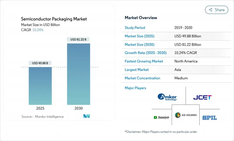
预计到 2025 年,半导体封装市场规模将达到 498.8 亿美元,到 2030 年将达到 812.2 亿美元,2025 年至 2030 年的复合年增长率为 10.24%。
从成本驱动型组装转向性能驱动型整合正在推动这一成长。人工智慧工作负载对高频宽记忆体和卓越散热路径的需求,正推动对2.5D和3D架构的快速需求。儘管产量仍依赖传统的引线键合和导线架工艺,但价值创造正转向扇出型晶圆层次电子构装(WLP)和支援晶片组的中介层。汽车电气化推动了高功率密度模组两位数的成长,而智慧型手机和PC的更新换代週期则维持了消费领域的基准产量。从区域来看,亚洲占全球产量的一半以上,但得益于《晶片法案》(CHIPS Act)的激励措施为新建后端晶圆厂提供的资金,北美地区的复合年增长率(CAGR)最高。 ABF基板的供应瓶颈和先进工具的出口限制,是推动地理多元化和材料创新的催化剂。
全球半导体封装市场趋势与洞察
AI加速器热潮推动2.5D/3D插层器的发展
台积电的CoWoS晶片产能将在2023年至2024年间翻一番,从12万片增加到24万片,但仍无法完全满足超大规模资料中心的需求。产能缺口促使业界探索替代性的面板级製程和3.5D堆迭测试,这些测试可将超过6000平方毫米的硅片整合到单一封装中。因此,先进封装技术正从成本中心转变为提升人工智慧系统效能的策略槓桿。
美国和亚洲的电动车动力组件
安森美半导体(ON Semiconductor)的EliteSiC平台已获大众汽车公司订单,该平台代表了向具有卓越散热性能的整合功率模组过渡的典范。罗姆(ROHM)的6合1模塑SiC模组的功率密度是传统型号的三倍。这些创新产品集中在美国和亚洲的供应链,使其能够满足严格的汽车认证标准。
ABF基板供应供不应求
Nittobo在2025年8月涨价20%,暴露出系统性的材料短缺问题,尤其对覆晶BGA生产线造成了严重影响。台湾和日本产能有限,导致前置作业时间延长,迫使OEM厂商考虑采用玻璃和硅芯替代方案。
细分市场分析
到2024年,传统的打线接合和导线架产品仍将占据半导体封装市场52.5%的份额(以出货量计),确保家用电子电器和工业设备的材料成本保持在可负担的范围内。然而,扇出型WLP(晶圆级封装)将以12.3%的复合年增长率超越所有其他封装形式,这标誌着半导体封装市场正向无基板的线路重布转型,从而降低z轴高度并提高I/O密度。覆晶将透过结合小间距凸点和适中的成本来填补这一市场空白,而SiP(系统级封装)和PoP(封装堆迭)架构则可实现垂直堆迭,从而满足空间受限的行动装置的需求。
在先进技术方面,2.5D中介层将高频宽记忆体与AI逻辑晶片并排放置,而3D堆迭技术则能有效降低延迟。嵌入式晶粒和麵板级生产线正吸引着专注于物联网价格分布的新兴参与企业,这标誌着半导体封装市场正在分化为高性能节点和超低成本量产厂商两大阵营。相较之下,面板级生产线的单脚价格低于0.10美元,凸显了成本结构的差异。因此,设备製造商正在对其产品组合进行细分,用于3µm对准的高精度键合机丛集与用于物联网标籤的大型面板模塑生产线并存。这种分化正在重新定义半导体封装市场中供应商的定位。
到2024年,有机ABF基板将占总收入的41.5%,为主流覆晶生态系统提供支援。然而,随着汽车和产业部门延长成熟的铝线和金线封装的使用寿命,键合线半导体封装市场规模预计将以每年11.4%的速度成长。导线架在重视铜散热器性能的功率应用中仍然很受欢迎。封装树脂正在朝向高导热等级发展,以支援下一代SiC和GaN模组。
2027年起,玻璃基板或将取代有机基板。英特尔和三星的原型产品展示了40%的通孔间距缩减和接近零的热膨胀係数失配,从而减少了3D堆迭中的翘曲。在1200V牵引逆变器中,奈米钻石填料被添加到导热界面材料中,可将结间电阻降低30%。 2025年,金价上涨将压缩显示器驱动IC封装的利润空间,进而推动铜柱凸点封装的普及。
区域分析
到2024年,亚洲将占据半导体封装市场53.0%的份额,这主要得益于台湾在CoWoS领域的领先地位以及中国在引线键合组装方面的规模优势。江电科技在江苏投资44亿元建造的汽车级工厂将提升当地碳化硅功率封装的产能。韩国受益于以记忆体为中心的SiP技术,而日本则在关键的基板化学领域占据主导地位,从而巩固了区域丛集的紧密联繫。
预计到2030年,北美半导体封装市场将以11.1%的复合年增长率成长。 《晶片封装法案》(CHIPS Act)的奖励措施已投资3亿美元用于研发,并在亚利桑那州、新墨西哥州和加州打造了研发中心。例如,台积电与安靠在亚利桑那州的伙伴关係,在领先的晶圆厂附近建立了完整的后端生态系统。加拿大正在大力发展光电封装,而墨西哥则为消费级ASIC晶片提供低成本的最终测试服务。
欧洲正巩固其在汽车和工业的优势。一家德国一级供应商正在共同开发一款双面冷却的碳化硅模组,目标是实现9kW/L的逆变器密度,这将推动对小众OSAT(外包半导体组装和测试)企业的投资。荷兰正积极推动高频光收发器的封装技术,以配合垂直共振腔面射型雷射(VCSEL)的普及应用。中东和非洲仍在发展中,目前主要将组装组装给亚洲的製造中心,但正计划根据主权指令,在国内建立用于安全物联网和国防电子产品的生产线。
其他福利:
- Excel格式的市场预测(ME)表
- 3个月的分析师支持
目录
第一章 引言
- 研究假设和市场定义
- 调查范围
第二章调查方法
第三章执行摘要
第四章 市场情势
- 市场概览
- 市场驱动因素
- AI加速器热潮推动2.5D/3D插层器的发展
- 美国和亚洲的电动车动力组件
- 美国和欧盟的晶片奖励催生了本地后端晶圆厂
- 中国和韩国对5G射频SiP的需求
- 面向物联网的超低成本面板级封装
- 用于高密度中介层的晶片组架构
- 市场限制
- ABF基板供不应求(台湾/日本)
- 3D TSV/混合键结中的产量比率挑战
- 中国对先进封装工具的出口限制
- 扇出型 WLP <5 nm 散热限制
- 价值/供应链分析
- 监理展望
- 技术展望
- 波特五力模型
- 供应商的议价能力
- 买方的议价能力
- 新进入者的威胁
- 替代品的威胁
- 竞争对手之间的竞争
- 产业能力与投资趋势分析
- 定价分析
第五章 市场规模与成长预测
- 透过包装平台
- 先进包装
- 覆晶
- 扇出 WLP
- 扇入式 WLP
- 2.5D/3D IC
- 嵌入式晶粒
- SiP/PoP
- 面板级包装
- 传统包装
- 引线键合
- 导线架
- QFN/QFP/SOP
- 先进包装
- 透过包装材料
- 有机基材物
- 导线架
- 连接线
- 封装树脂
- 陶瓷包装
- 焊球和焊点凸起
- 晶片黏接和导热硅脂
- 按晶圆尺寸
- 200毫米或更小
- 300 mm
- 450毫米或以上/面板
- 按经营模式
- OSAT
- 晶圆代工厂后端
- IDM内部
- 按最终用户行业划分
- 消费性电子产品
- 智慧型手机和穿戴式装置
- 计算/资料中心
- 汽车与出行
- ADAS/EV动力
- 通讯和电讯
- 5G基础设施
- 航太与国防
- 医疗和保健设备
- 工业/能源(LED/电力)
- 消费性电子产品
- 按地区
- 北美洲
- 美国
- 加拿大
- 墨西哥
- 南美洲
- 巴西
- 其他南美洲
- 欧洲
- 德国
- 法国
- 英国
- 义大利
- 荷兰
- 北欧国家
- 其他欧洲地区
- 中东和非洲
- 以色列
- 土耳其
- GCC
- 南非
- 其他中东和非洲地区
- 亚太地区
- 中国
- 台湾
- 韩国
- 日本
- 印度
- 新加坡
- 澳洲
- 纽西兰
- 亚太其他地区
- 北美洲
第六章 竞争情势
- 市场集中度
- 策略趋势
- 市占率分析
- 公司简介
- ASE Technology Holding Co., Ltd.
- Amkor Technology, Inc.
- JCET Group Co., Ltd.
- Siliconware Precision Industries Co., Ltd.
- Powertech Technology Inc.
- Tianshui Huatian Technology Co., Ltd.
- UTAC Holdings Ltd.
- ChipMOS Technologies Inc.
- Chipbond Technology Corp.
- Intel Corporation
- Samsung Electronics Co., Ltd.
- Taiwan Semiconductor Manufacturing Co. Ltd.(TSMC)
- Micron Technology, Inc.
- Texas Instruments Inc.
- Advanced Micro Devices, Inc.
- Hana Micron Inc.
- Nepes Corporation
- TongFu Microelectronics Co., Ltd.
- Shinko Electric Industries Co., Ltd.
- Unisem(M)Berhad
第七章 市场机会与未来展望
The semiconductor packaging market size stood at USD 49.88 billion in 2025 and is projected to reach USD 81.22 billion by 2030, advancing at a 10.24% CAGR over 2025-2030.
A shift from cost-driven assembly toward performance-critical integration underpins this growth. Demand for 2.5D and 3D architectures has risen sharply as AI workloads call for high-bandwidth memory and superior thermal paths. Volume remains anchored in traditional wire-bond and lead-frame formats, yet value creation is migrating to fan-out wafer-level packaging (WLP) and chiplet-enabled interposers. Automotive electrification supports double-digit expansion in power-dense modules, while smartphone and PC refresh cycles sustain baseline volumes in the consumer segment. Regionally, Asia commands more than half of global output, but North America registers the highest CAGR thanks to CHIPS Act incentives that fund new back-end fabs. Supply bottlenecks in ABF substrates and export restrictions on advanced tools are catalyzing geographic diversification and material innovation.
Global Semiconductor Packaging Market Trends and Insights
AI accelerator boom driving 2.5D/3D interposers
TSMC's CoWoS capacity is doubling from 120,000 to 240,000 units between 2023 and 2024, yet it still cannot fully meet hyperscaler demand. The capacity gap is stimulating alternative panel-level flows and 3.5D stacking trials that aggregate more than 6,000 mm2 of silicon per package. Advanced packaging has therefore moved from a cost center to a strategic lever for AI system performance
Electrified-vehicle power packages in United States & Asia
onsemi's EliteSiC platform awarded by Volkswagen exemplifies the migration toward integrated power modules with superior heat dissipation. ROHM's 6-in-1 molded SiC modules deliver triple the power density of prior. These innovations concentrate in US and Asian supply chains that can meet stringent automotive qualification.
ABF substrate supply crunch
Nittobo's 20% price hike in August 2025 exposes systemic material tightness that particularly affects flip-chip BGA lines. Limited qualified capacity in Taiwan and Japan prolongs lead times and pushes OEMs to explore glass-core or silicon-core alternatives.
Other drivers and restraints analyzed in the detailed report include:
- US-EU CHIPS incentives creating local back-end fabs
- 5G RF-SiP demand in China & Korea
- Yield challenges in 3D TSV/hybrid bonding
For complete list of drivers and restraints, kindly check the Table Of Contents.
Segment Analysis
Traditional wire-bond and lead-frame offerings still dominated shipments with 52.5% semiconductor packaging market share in 2024, ensuring that consumer electronics and industrial devices retain affordable bill-of-materials costs. However, Fan-out WLP outpaces every other format at a 12.3% CAGR, signaling the semiconductor packaging market's move toward substrate-free redistribution layers that shrink z-height and boost I/O density. Flip-chip bridges the gap by pairing fine-pitch bumps with moderate cost, while SiP and PoP architectures enable vertical stacking for space-constrained handsets.
On the advanced front, 2.5D interposers position high-bandwidth memory adjacent to AI logic, and 3D stacks unlock latency gains. Embedded-die and panel-level flows attract new entrants focused on IoT price points, demonstrating that the semiconductor packaging market is splitting into premium performance nodes and ultra-low-cost volume plays. In contrast, panel-level lines deliver sub-USD 0.10 per pin, a ratio that underscores divergent cost structures. As a result, equipment makers have segmented their portfolios: high-accuracy bonder clusters for 3 µm alignment coexist with large-panel MOLD lines aimed at IoT tags. Such bifurcation redefines supplier positioning inside the semiconductor packaging market.
Organic ABF substrates carried 41.5% revenue in 2024, underpinning the mainstream flip-chip ecosystem. Yet semiconductor packaging market size for bonding wires is set to grow 11.4% annually as automotive and industrial sectors extend the life of proven aluminum and gold wire packages. Leadframes persist in power applications that value copper heat-spreader performance. Encapsulation resins have progressed to high-thermal-conductivity grades, supporting next-generation SiC and GaN modules.
Glass substrates could displace organic builds after 2027. Intel and Samsung prototypes show 40% via pitch reduction and near-zero CTE mismatch, lowering warpage in 3D stacks. Thermal interface materials now integrate nano-diamond fillers, cutting junction-to-case resistance by 30% in 1,200 V traction inverters. Gold price spikes compressed margins for display driver IC packaging in 2025, motivating migration to copper column bumps
The Semiconductor Packaging Market is Segmented by Packaging Platform (Advanced Packaging, Traditional Packaging), Packaging Material (Organic Substrates, and More), Wafer Size (<= 200 Mm, and More), Business Model (OSAT, and More) End-User Industry (Consumer Electronics, Aerospace and Defense and More), and by Geography. The Market Forecasts are Provided in Terms of Value (USD).
Geography Analysis
Asia captured 53.0% of the semiconductor packaging market in 2024, cemented by Taiwan's CoWoS monopoly and China's scale in wire-bond assembly. JCET's RMB 4.4 billion automotive plant in Jiangsu advances local competency in SiC power packages. South Korea benefits from memory-centric SiP, whereas Japan controls pivotal substrate chemistries, reinforcing a tightly knit regional cluster.
North America's semiconductor packaging market is projected to post an 11.1% CAGR through 2030. CHIPS Act incentives amass USD 300 million for R&D lines, spawning hubs in Arizona, New Mexico and California. Partnerships such as TSMC-Amkor in Arizona build complete back-end ecosystems proximate to leading-edge wafer fabs. Canada cultivates photonics packaging, and Mexico offers low-cost final test for consumer ASICs.
Europe positions around automotive and industrial strength. German Tier-1s co-develop double-sided cooled SiC modules targeting 9 kW/L inverter density, catalyzing niche OSAT investment. The Netherlands pushes high-frequency optical transceiver packaging that aligns with vertical-cavity surface-emitting laser (VCSEL) adoption. Middle East and Africa remain emerging, primarily outsourcing assembly to Asian hubs yet planning domestic lines for secure IoT and defense electronics under sovereign mandates.
- ASE Technology Holding Co., Ltd.
- Amkor Technology, Inc.
- JCET Group Co., Ltd.
- Siliconware Precision Industries Co., Ltd.
- Powertech Technology Inc.
- Tianshui Huatian Technology Co., Ltd.
- UTAC Holdings Ltd.
- ChipMOS Technologies Inc.
- Chipbond Technology Corp.
- Intel Corporation
- Samsung Electronics Co., Ltd.
- Taiwan Semiconductor Manufacturing Co. Ltd. (TSMC)
- Micron Technology, Inc.
- Texas Instruments Inc.
- Advanced Micro Devices, Inc.
- Hana Micron Inc.
- Nepes Corporation
- TongFu Microelectronics Co., Ltd.
- Shinko Electric Industries Co., Ltd.
- Unisem (M) Berhad
Additional Benefits:
- The market estimate (ME) sheet in Excel format
- 3 months of analyst support
TABLE OF CONTENTS
1 INTRODUCTION
- 1.1 Study Assumptions and Market Definition
- 1.2 Scope of the Study
2 RESEARCH METHODOLOGY
3 EXECUTIVE SUMMARY
4 MARKET LANDSCAPE
- 4.1 Market Overview
- 4.2 Market Drivers
- 4.2.1 AI Accelerator Boom Driving 2.5D/3D Interposers
- 4.2.2 Electrified Vehicle Power Packages in United States and Asia
- 4.2.3 US-EU CHIPS Incentives Creating Local Back-End Fabs
- 4.2.4 5G RF-SiP Demand in China and Korea
- 4.2.5 Panel Level Packaging for Ultra-Low-Cost IoT
- 4.2.6 Chiplet Architectures Powering High-Density Interposers
- 4.3 Market Restraints
- 4.3.1 ABF Substrate Supply Crunch (Taiwan/Japan)
- 4.3.2 Yield Challenges in 3D TSV/Hybrid Bonding
- 4.3.3 Export Controls on Advanced Packaging Tools to China
- 4.3.4 Thermal Dissipation Limits in Fan-Out WLP <5 nm
- 4.4 Value / Supply-Chain Analysis
- 4.5 Regulatory Outlook
- 4.6 Technological Outlook
- 4.7 Porter's Five Forces
- 4.7.1 Bargaining Power of Suppliers
- 4.7.2 Bargaining Power of Buyers
- 4.7.3 Threat of New Entrants
- 4.7.4 Threat of Substitutes
- 4.7.5 Intensity of Competitive Rivalry
- 4.8 Industry Capacity and Investment Trend Analysis
- 4.9 Pricing Analysis
5 MARKET SIZE AND GROWTH FORECASTS (VALUE)
- 5.1 By Packaging Platform
- 5.1.1 Advanced Packaging
- 5.1.1.1 Flip-Chip
- 5.1.1.2 Fan-Out WLP
- 5.1.1.3 Fan-In WLP
- 5.1.1.4 2.5D / 3D IC
- 5.1.1.5 Embedded-Die
- 5.1.1.6 SiP / PoP
- 5.1.1.7 Panel-Level Packaging
- 5.1.2 Traditional Packaging
- 5.1.2.1 Wire-Bond
- 5.1.2.2 Leadframe
- 5.1.2.3 QFN / QFP / SOP
- 5.1.1 Advanced Packaging
- 5.2 By Packaging Material
- 5.2.1 Organic Substrates
- 5.2.2 Leadframes
- 5.2.3 Bonding Wires
- 5.2.4 Encapsulation Resins
- 5.2.5 Ceramic Packages
- 5.2.6 Solder Balls and Bumps
- 5.2.7 Die-Attach and TIMs
- 5.3 By Wafer Size
- 5.3.1 <= 200 mm
- 5.3.2 300 mm
- 5.3.3 >= 450 mm / Panel
- 5.4 By Business Model
- 5.4.1 OSAT
- 5.4.2 Foundry Back-End
- 5.4.3 IDM In-house
- 5.5 By End-user Industry
- 5.5.1 Consumer Electronics
- 5.5.1.1 Smartphones and Wearables
- 5.5.1.2 Computing / Data-Center
- 5.5.1.3 Automotive and Mobility
- 5.5.1.3.1 ADAS / EV Power
- 5.5.1.4 Communications and Telecom
- 5.5.1.4.1 5G Infrastructure
- 5.5.1.5 Aerospace and Defense
- 5.5.1.6 Medical and Healthcare Devices
- 5.5.1.7 Industrial and Energy (LED / Power)
- 5.5.1 Consumer Electronics
- 5.6 By Geography
- 5.6.1 North America
- 5.6.1.1 United States
- 5.6.1.2 Canada
- 5.6.1.3 Mexico
- 5.6.2 South America
- 5.6.2.1 Brazil
- 5.6.2.2 Rest of South America
- 5.6.3 Europe
- 5.6.3.1 Germany
- 5.6.3.2 France
- 5.6.3.3 United Kingdom
- 5.6.3.4 Italy
- 5.6.3.5 Netherlands
- 5.6.3.6 Nordics
- 5.6.3.7 Rest of Europe
- 5.6.4 Middle East and Africa
- 5.6.4.1 Israel
- 5.6.4.2 Turkey
- 5.6.4.3 GCC
- 5.6.4.4 South Africa
- 5.6.4.5 Rest of Middle East and Africa
- 5.6.5 APAC
- 5.6.5.1 China
- 5.6.5.2 Taiwan
- 5.6.5.3 South Korea
- 5.6.5.4 Japan
- 5.6.5.5 India
- 5.6.5.6 Singapore
- 5.6.5.7 Australia
- 5.6.5.8 New Zealand
- 5.6.5.9 Rest of APAC
- 5.6.1 North America
6 Competitive Landscape
- 6.1 Market Concentration
- 6.2 Strategic Moves
- 6.3 Market Share Analysis
- 6.4 Company Profiles (includes Global level Overview, Market level overview, Core Segments, Financials as available, Strategic Information, Market Rank/Share, Products & Services, Recent Developments)
- 6.4.1 ASE Technology Holding Co., Ltd.
- 6.4.2 Amkor Technology, Inc.
- 6.4.3 JCET Group Co., Ltd.
- 6.4.4 Siliconware Precision Industries Co., Ltd.
- 6.4.5 Powertech Technology Inc.
- 6.4.6 Tianshui Huatian Technology Co., Ltd.
- 6.4.7 UTAC Holdings Ltd.
- 6.4.8 ChipMOS Technologies Inc.
- 6.4.9 Chipbond Technology Corp.
- 6.4.10 Intel Corporation
- 6.4.11 Samsung Electronics Co., Ltd.
- 6.4.12 Taiwan Semiconductor Manufacturing Co. Ltd. (TSMC)
- 6.4.13 Micron Technology, Inc.
- 6.4.14 Texas Instruments Inc.
- 6.4.15 Advanced Micro Devices, Inc.
- 6.4.16 Hana Micron Inc.
- 6.4.17 Nepes Corporation
- 6.4.18 TongFu Microelectronics Co., Ltd.
- 6.4.19 Shinko Electric Industries Co., Ltd.
- 6.4.20 Unisem (M) Berhad
7 MARKET OPPORTUNITIES AND FUTURE OUTLOOK
- 7.1 White-space and Unmet-Need Assessment
 3-D TSV:关键问题洞察与市场分析
 半导体原型製作和封装市场分析及预测(至 2034 年):类型、产品、服务、技术、应用、材料类型、组件、流程、最终用户、设备
 高密度封装(MCM、MCP、SIP、3D-TSV):市场分析与技术趋势
 全球 3D 半导体封装市场:未来预测(至 2032 年)—材料、技术、最终用户和地区分析
 2025年先进晶片封装全球市场报告2025年全球3D半导体封装市场报告
 半导体先进封装市场(按平台、材料类型、组件、间距、应用和最终用途行业)- 全球预测,2025 年至 2030 年2025年全球四方扁平封装市场报告先进晶片封装市场(按封装类型和地区)
 日本半导体封装市场规模、份额、趋势及预测(按类型、封装材料、技术、最终用户和地区),2025 年至 2033 年