


 |
市场调查报告书
商品编码
1478709
高密度封装(MCM、MCP、SIP、3D-TSV):市场分析与技术趋势High-Density Packaging (MCM, MCP, SIP, 3D-TSV): Market Analysis and Technology Trends |
||||||
在快速发展的半导体产业中,先进封装处于创新的前沿,推动着从高效能运算到消费性电子产品等广泛应用的下一波效能改进和整合能力。随着设备变得越来越小、越来越复杂,传统封装技术正在达到其物理和功能极限。
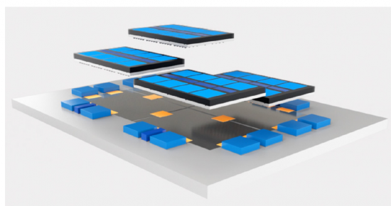
人工智慧(AI)、5G 通讯、汽车电子和物联网(IoT) 等技术的出现正在迅速推动对晶片的需求,这些晶片需要在日益紧凑的封装中提供更高的性能、更低的功耗和更强大的功能。为了解决这个问题,3D 整合、小晶片、扇出晶圆级封装 (FOWLP) 和硅通孔 (TSV) 等先进封装技术已成为关键推动因素,使前所未有的整合度和系统复杂性成为可能。这些创新不仅克服了传统缩放的限制,而且在电路设计、系统架构和材料科学方面开闢了新途径,预示着半导体能力的新时代。
在快速发展的半导体製造领域,先进封装技术在开发高性能、紧凑型和节能电子设备方面发挥着至关重要的作用。Forboros 拥有多种先进封装技术,其中包括扇出晶圆级封装 (FOWLP)、硅通孔 (TSV)、高频宽记忆体 (HBM)、晶圆基板上晶片 (CoWoS)。
本报告深入探讨了半导体先进封装的现状,深入瞭解最新的技术进步、材料创新和製程改进。我们审视竞争格局,专注于关键参与者及其策略举措,以获取市场占有率并推动行业标准。此外,它还评估了全球供应链动态、监管环境和地缘政治因素对先进封装市场的影响,使利害关係人能够全面瞭解即将到来的课题和机会。
目录
第一章简介
第二章执行摘要
第三章技术问题与趋势
- HDP技术概述
- 2D封装
- 2.5D 和 3D 包
第4章 应用
- 半导体产业终端市场
- 记忆
- 铸造部
第五章竞争环境
- 高密度聚乙烯製造商
第6章 3D-TSV技术
- 3D-TSV 驱动因素
- 3D 封装类型
- 硅通孔工艺
- 重要加工技术
- 用法
- 3D封装技术的局限性
- 公司简介
第七章 市场预测
- 先进封装概述
- 促进因素
- 系统级封装 (SiP)
- 倒装晶片/晶圆级封装
- 全球IC市场预测
- 全球包装市场预测
- 全球先进封装预测
Introduction
In the rapidly evolving semiconductor industry, advanced packaging stands at the forefront of innovation, driving the next wave of performance enhancements and integration capabilities across a broad spectrum of applications, from high-performance computing to consumer electronics. As devices shrink in size yet grow in complexity, traditional packaging techniques are reaching their physical and functional limits, prompting the industry to adopt more sophisticated, efficient, and cost-effective solutions. This comprehensive report delves into the intricate world of semiconductor advanced packaging, exploring the latest trends, technologies, and market dynamics shaping the future of this critical sector.
The advent of technologies such as artificial intelligence (AI), 5G communications, automotive electronics, and the Internet of Things (IoT) has precipitated a surge in demand for chips that offer higher performance, lower power consumption, and greater functionality, all within increasingly compact footprints. In response, advanced packaging technologies such as 3D integration, chiplets, fan-out wafer-level packaging (FOWLP), and through-silicon vias (TSVs) have emerged as key enablers, allowing for unprecedented levels of integration and system complexity. These innovations not only overcome the limitations of traditional scaling but also open new avenues for circuit design, system architecture, and material science, heralding a new era of semiconductor functionality.
This report provides a deep dive into the state of the art in semiconductor advanced packaging, offering insights into the latest technological advancements, material innovations, and process improvements. It examines the competitive landscape, highlighting the key players and their strategic initiatives to capture market share and drive industry standards. Moreover, the report assesses the impact of global supply chain dynamics, regulatory environments, and geopolitical factors on the advanced packaging market, providing stakeholders with a comprehensive understanding of the challenges and opportunities ahead.
About This Report
In the rapidly evolving landscape of semiconductor manufacturing, advanced packaging technologies play a pivotal role in enabling the development of high-performance, compact, and energy-efficient electronic devices. Among the myriad of advanced packaging techniques, fan-out wafer-level packaging (FOWLP), through-silicon vias (TSVs), High Bandwidth Memory (HBM), Chip-on-Wafer-on-Substrate (CoWoS), and Foveros have emerged as key innovations revolutionizing the industry. This essay delves into these advanced packaging technologies, exploring their principles, applications, benefits, and impact on the semiconductor ecosystem.
Fan-Out Wafer-Level Packaging (FOWLP):
Fan-out wafer-level packaging (FOWLP) is a cutting-edge packaging technique that offers superior performance, increased functionality, and enhanced miniaturization compared to traditional packaging methods. In FOWLP, the semiconductor die is embedded within a polymer matrix, and redistribution layers (RDLs) are used to redistribute the I/Os to the package perimeter.
Through-Silicon Vias (TSVs):
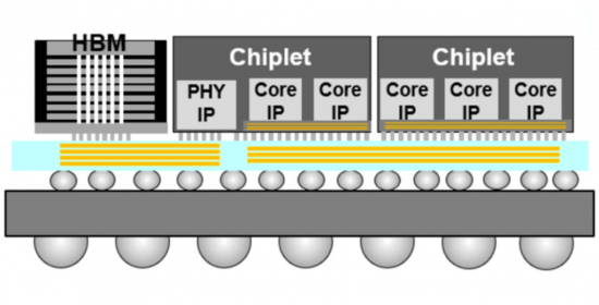
Through-silicon vias (TSVs) are vertical electrical interconnects that traverse through the silicon substrate, enabling multi-die stacking and 3D integration. TSVs facilitate the vertical integration of heterogeneous devices, such as logic, memory, and sensors, on a single silicon substrate, thereby reducing interconnect length, improving performance, and conserving space. TSVs are instrumental in advanced packaging technologies like 3D stacked memory, system-on-chip (SoC) integration, and interposer-based packaging, driving innovations in high-performance computing, artificial intelligence, and networking applications.
High Bandwidth Memory (HBM):
High Bandwidth Memory (HBM) is an advanced memory technology that leverages vertical stacking and TSVs to achieve unprecedented levels of memory bandwidth and energy efficiency. HBM utilizes multiple DRAM dies vertically stacked on top of each other and interconnected through TSVs, allowing for significantly higher memory bandwidth compared to traditional memory architectures. HBM is widely used in graphics cards, data centers, and highperformance computing systems, where memory bandwidth and power efficiency are critical for handling large datasets and complex workloads.
Chip-on-Wafer-on-Substrate (CoWoS):
Chip-on-Wafer-on-Substrate (CoWoS) is a packaging technology developed by TSMC that enables the integration of multiple silicon dies on a single substrate, or interposer. In CoWoS, individual chips are fabricated on separate wafers and then bonded onto a silicon interposer using microbumps and TSVs. This allows for heterogeneous integration of different functional blocks, such as logic, memory, and analog, on a single package, enabling higher levels of performance, power efficiency, and system-level integration. CoWoS is widely used in highperformance computing, networking, and AI accelerators, where heterogeneous integration is essential for achieving optimal performance and functionality.
Foveros:
Foveros is an advanced packaging technology developed by Intel that enables 3D stacking of logic dies, memory dies, and other components to create highly integrated and compact semiconductor packages. In Foveros, individual dies are fabricated separately and then stacked vertically using microbumps and TSVs, allowing for dense integration of heterogeneous components with minimal footprint. Foveros enables innovative form factors, such as chiplets and system-in-package (SiP), and facilitates the development of power-efficient, highperformance devices for a wide range of applications, including mobile computing, IoT, and edge computing.
The Need for This Report
Investing in a semiconductor advanced packaging report offers several compelling reasons, each of which contributes to enhancing your understanding of the industry and making informed decisions. Here's why you should consider purchasing such a report:
Industry Insights: A semiconductor advanced packaging report provides comprehensive insights into the latest trends, developments, and innovations shaping the semiconductor packaging landscape. It offers valuable information on emerging technologies, market dynamics, and competitive landscape, helping you stay updated with the latest industry advancements.
Market Analysis: The report offers in-depth analysis of the semiconductor packaging market, including market size, growth potential, and key drivers and challenges. It provides detailed segmentation by packaging type, application, and region, for FOWLP, through-silicon vias (TSVs), and 3D integration, as well as AI-based technologies including HBM3, CoWoS, and Foveros.
Competitive Intelligence: By examining the strategies, product portfolios, and market positioning of key players in the semiconductor packaging industry, the report offers valuable competitive intelligence. It helps you benchmark your company's performance against industry leaders, identify potential collaborators or acquisition targets, and develop effective market entry or expansion strategies.
Technology Trends: Semiconductor advanced packaging reports delve into the latest technological advancements and innovations in packaging techniques such as fan-out waferlevel packaging (FOWLP), through-silicon vias (TSVs), and 3D integration, as well as AI-based technologies including HBM3, CoWoS, and Foveros. By understanding the evolving technological landscape, you can anticipate future trends, align your R&D efforts with market demands, and gain a competitive edge in the industry.
Investment Opportunities: Armed with comprehensive market insights and competitive analysis, a semiconductor advanced packaging report enables you to identify attractive investment opportunities across different segments of the semiconductor packaging market. Whether you're a semiconductor manufacturer, equipment supplier, or investor, the report provides valuable guidance for making strategic investment decisions and maximizing returns on investment.
Table of Contents
Chapter 1. Introduction
Chapter 2. Executive Summary
- 2.1. Summary of Technology Issues
- 2.2. Summary of Market Forecasts
Chapter 3. Technology Issues and Trends
- 3.1. Overview of HDP Technology
- 3.1.1. Need for Multiple IC Integration
- 3.1.2. Challenges of Multiple IC Integration
- 3.1.3. Technical Constraints of Integration
- 3.1.4. Economic Benefits of HDP
- 3.1.5. Technology Issues
- 3.2 2D Packages
- 3.2.1. MCMs
- 3.2.1.1. Substrates
- 3.2.1.2. Thermal Management
- 3.2.1.3. Design
- 3.2.1.4. Known Good Die
- 3.2.2. System In Package (SiP)
- 3.2.2.1. SiP Challenges
- 3.2.2.2. Cost
- 3.2.2.3. SiP Design
- 3.2.2.4. SoC Versus SiP
- 3.2.3. Multichip Package (MCP)
- 3.2.4. Package-On-Package (PoP)
- 3.2.1. MCMs
- 3.3 2.5D and 3D Packages
- 3.3.1. Conventional Wafer Fan-Out Technologies
- 3.3.2. Silicon Interposers
- 3.3.3. 3D-IC Stacks
Chapter 4. Applications
- 4.1. Semiconductor Industry by End Market
- 4.2. Memory
- 4.2.1. DRAM
- 4.2.2. NAND
- 4.2.3. China Memory
- 4.2.4. HDD vs SSD
- 4.3. Foundry Sector
Chapter 5. Competitive Environment
- 5.1. HDP Manufacturers
Chapter 6 3-D-TSV Technology
- 6.1. Driving Forces In 3D-TSV
- 6.2 3-D Package Varieties
- 6.3. TSV Processes
- 6.4. Critical Processing Technologies
- 6.4.1. Plasma Etch Technology
- 6.4.2. Cu Plating
- 6.4.3. Thin Wafer Bonding
- 6.4.4. Wafer Thinning/CMP
- 6.4.5. Lithography
- 6.5. Applications
- 6.6. Limitations Of 3-D Packaging Technology
- 6.6.1. Thermal Management
- 6.6.2. Cost
- 6.6.3. Design Complexity
- 6.6.4. Time To Delivery
- 6.7. Company Profiles
Chapter 7. Market Forecast
- 7.1. Overview of Advanced Packages
- 7.2. Driving Forces
- 7.3. System-in-Package (SiP)
- 7.4. Flip Chip/Wafer Level Packaging
- 7.5. Worldwide IC Market Forecast
- 7.6. Worldwide Packaging Market Forecast
- 7.7. Worldwide Advanced Package Forecast
- 7.7.1. Worldwide 3-D Through Silicon Via (TSV) Market
- 7.7.1.1. TSMC CoWoS
- 7.7.1.2. Intel Foveros
- 7.7.1.3. HBM (High Bandwidth Memory) Packages
- 7.7.1.4. Chiplets
- 7.7.1. Worldwide 3-D Through Silicon Via (TSV) Market
List of Tables
- 3.1. Multichip Modules Vs. Circuit Board Assemblies
- 3.2. MCM Cost Comparison
- 3.3. Materials Challenge For Packaging
- 3.4. Substrate Technology Features
- 3.5. Comparison of SoC and SiP Architectures
- 3.6. Comparison of CSP and PoP Architectures
- 4.1. Global Semiconductor Forecast By End Market
- 4.2. Global Semiconductor Revenue Forecast By Device Type
- 4.3. Global Semiconductor Unit Forecast By Device Type
- 4.4. DRAM Supply
- 4.5. DRAM Demand
- 4.6. DRAM Revenues
- 4.7. NAND Supply
- 4.8. NAND Supply-Demand
- 4.9. NAND Unit Demand By Application
- 4.10. NAND Revenues
- 4.11. Comparison Of HDD and SSD For Storage
- 4.12. Foundry Market Forecast
- 4.13. Comparison Of Foundry Capacities
- 5.1. MCM Manufacturers
- 6.1. 3-D Mass Memory Volume Comparison Between Other Technologies and TI's 3D Technology In Cm3/Gbit
- 6.2. 3-D Mass Memory Weight Comparison Between Other Technologies and TI's 3D Technology In Grams3/Gbit
- 7.1. Semiconductor Forecast by Revenues
- 7.2. Worldwide IC Package Market Forecast
- 7.3. Worldwide Advanced Package Market
- 7.4. TSMC'S CoWoS Revenue Analysis
- 7.5. HBM TAM Demand 2023-2026
List of Figures
- 1.1. Schematic Cross-Section View Of An MCM-D
- 1.2. Cross-Section Of The RF And Microwave MCM-D Structure
- 1.3. Thin Film Layers On The Planarized Core Layer Of MCM-SL/D Technology
- 1.4. Flip Chip MCP
- 1.5. SIP Cross Section
- 3.1. IC Packaging Trends
- 3.2. Technology Tree For HDP Types
- 3.3. Form Factor Decrease By Package Type
- 3.4. Wafer Level Packaging Processing Line
- 3.5. TSMC's InFO
- 3.6. SLIM and SWIFT Package Definition
- 4.1. Global Semiconductor Forecast By End Market
- 4.2. DRAM Roadmap By Die Shrink
- 4.3. 3D NAND Roadmap By Die Layers
- 4.4. HDD and SSD Shipments Forecast
- 4.5. HDD and SSD ASP
- 4.6. HDD and SSD Zetabytes
- 4.7. Pure-Play Foundry Market Shares
- 6.1. 3-D Technology On DRAM Density
- 6.2. 3-D Through-Silicon Via (TSV)
- 6.3. Graphical Illustration Of The Silicon Efficiency Between MCMs And 3D Technology
- 6.4. Silicon Efficiency Comparison Between 3D Packaging Technology And Other Conventional Packaging Technologies
- 6.5. 3D Packages
- 6.6. Via First, Middle, And Last Process Flows
- 6.7. Via First TSV Process Flow
- 6.8. New Applications Driving TSV Growth
- 6.9. Projection Of TSV Applications And Process Requirements
- 6.10. 3-D Technology For DRAM
- 6.11. Moore's Law For Active Element Density
- 7.1. Various System-In-Package (SiP) Applications
- 7.2. SiP Structures
- 7.3. Wire Bond Versus Flip Chip
- 7.4. Flip Chip And Wire Bond Equipment Forecast
- 7.5. Growth In Copper Wire Bonding
- 7.6. UNIT SHIPMENTS OF SEMICONDUCTORS
- 7.7. WLP Demand By Devices
- 7.8. Device Shipment Forecast FIWLP vs FOWLP
- 7.9. WLP Demand By Wafers
- 7.10. Projection of 3-D TSV Applications And Process Requirement
- 7.11. Market Forecast of 3-D TSV Units
- 7.12. Market Forecast of 3-D TSV Wafers
- 7.13. TSMC's CoWoS Advanced Package
- 7.14. TSMC's CoWoS Advanced Package Revenues
- 7.15. SK hynix HBM3 Package
 全球防静电载带捲市场(按载带类型、材料、胶带材料成分、胶带层数和最终用途产业划分)预测(2026-2032年)导线架固定胶带市场(按黏合剂类型、背衬材料、胶带宽度、胶带厚度、应用、最终用途行业和销售管道),全球预测,2026-2032年
 MEMS封装焊料市场规模、份额和成长分析:按焊料类型、产品形式、应用、封装类型、最终用户和地区划分 - 2026-2033年产业预测
 先进半导体封装市场分析及预测(至2035年):依类型、产品类型、服务、技术、应用、材料类型、装置、製程、最终用户及功能划分半导体原型製作及封装市场分析及预测(至2035年):依类型、产品类型、服务、技术、应用、材料类型、组件、製程、最终用户、设备划分半导体封装市场分析及预测(至2035年):依类型、产品类型、技术、应用、材料类型、装置、製程、最终用户、功能、设备划分
 高端半导体封装:市场占有率分析、产业趋势与统计、成长预测(2026-2031)
 3-D TSV:关键问题洞察与市场分析
 2026年全球四方扁平包装市场报告先进晶片封装全球市场报告,2026年