


 |
市场调查报告书
商品编码
1849992
光电子:市场份额分析、行业趋势、统计数据和成长预测(2025-2030 年)Optoelectronics - Market Share Analysis, Industry Trends & Statistics, Growth Forecasts (2025 - 2030) |
||||||
※ 本网页内容可能与最新版本有所差异。详细情况请与我们联繫。
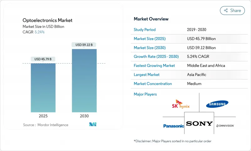
预计2025年光电市场规模将达457.9亿美元,2030年将达591.2亿美元,复合年增长率为5.24%。
需求广泛,涵盖消费性设备中的下一代3D感测、人工智慧密集型资料中心的高速光链路以及电动车中的先进照明和成像系统。装置创新受惠于能够在更高频率和温度下高效运作的宽能带隙材料,亚洲和北美的政策奖励也鼓励区域製造,以增强供应链的韧性。能够整合超表面光学元件和多结VCSEL架构的公司将占据先机,尤其是在功率效率和紧凑外形尺寸成为关键驱动因素的情况下。在所有最终用途中,买家越来越多地评估供应商是否能够证明关键投入的可追溯来源以及是否符合新兴的出口管制法规。
全球光电市场趋势与洞察
基于 VCSEL 的 3D 感测技术在亚洲智慧型手机的渗透率
随着安全人脸部认证、空间视讯捕捉和室内导航需求的不断增长,垂直共振腔面射型雷射(VCSEL) 在旗舰设备中的作用也日益增强。中国供应商提交的专利申请表明,他们正致力于全面实现 VCSEL 迭层国产化,并减少对进口外延晶圆的依赖。拥有高产量比率外延生长和先进测试能力的组件製造商已在屏下 3D 感测部署之前签署了多年期供应协议。随着光学 AI 协处理器的成熟,光电市场预计将在中阶行动电话中广泛采用支援 VCSEL 的手势和环境映射技术。
欧洲对汽车LED照明的严格要求
欧盟 (EU) 安全标准建议使用自我调整LED 头灯,以最大程度减少眩光并提升夜间驾驶舒适度,这促使汽车製造商采用先进的光域控制器。一级供应商正积极响应,推出 RGB 矩阵,以实现动态光束整形、品牌标誌性动画和节能效果,从而延长电动车的续航里程。设计週期越来越需要照明和热管理团队之间的密切合作,以在不增加冷却品质的情况下实现流明输出和监管目标。这项法规间接促进了光电市场的发展,因为模组中嵌入的微光学元件、驱动器和感测器的价值超越了 LED晶粒本身。获得欧洲车型认证的全球汽车製造商倾向于将相同的先进照明套件扩展到其他地区,从而推动了单位需求。
长期GaN基板供应限制
自主型GaN晶圆的生产仍然集中在少数几家专业工厂,这为高功率元件的生产带来了瓶颈。一些暂时的变通方案,例如在硅片上生长GaN,有助于降低成本,但会引入位错密度,从而限制额定电压。政府现在将宽能带隙基板视为关键资产,为国内晶体生长工厂提供扣除额,以降低战略风险。像Qromis基板技术这样的先驱方法将异质外延堆迭技术应用于200毫米晶圆,有望实现更高的产量并与主流晶圆厂更好地相容。虽然这些措施将在中期内提高产能,但短期产能短缺仍将推动电动车和国防项目的优先发展。
細項分析
由于园艺照明、汽车外部模组和商用显示器市场的復苏,LED 将在 2024 年继续保持其在光电市场的领先地位,占总营收的 34%。该细分市场受益于成熟的生产线和晶片级改进,这些改进无需大量资本支出即可提高每瓦流明。同时,受 3D 感测、短距离光互连和汽车雷射雷达 (LiDAR) 日益普及的推动,雷射二极体(尤其是垂直共振器和边缘发射结构)的复合年增长率达到 6.8%。多结架构可以在相同的晶粒面积上提取更多光功率。随着行动电话製造商青睐承包发送器封装,将晶圆级测试与整合式驱动器 IC 结合的供应商将继续获得设计优势。
人们对超表面整合日益增长的兴趣,放大了晶片表面精确光束整形的价值,从而增加了目标商标产品製造商的转换成本。随着超表面库的成熟,雷射二极体设计人员正在将定製图形化融入最终的外延工艺中,实现传统透镜无法实现的图案和相位控制。客製化发散分布的能力将释放企业对扩增实境(AR)显示器和短焦投影机的需求,从而扩大整个可寻址光电子市场。虽然LED仍然是大面积照明的关键,但雷射二极体正在开闢一个需要连贯光和精确光束控制的高端市场。
氮化镓凭藉其卓越的电子迁移率和热导率,能够在快速开关速度下高效运行,并将在2024年占据41%的市场份额,继续在光电子市场占据主导地位。晶圆尺寸缩小至200毫米将有助于降低成本,而合金工程技术则能够将光发射范围从紫外线调整到可见光,以实现感测和杀菌。然而,碳化硅将呈现最快的成长轨迹,复合年增长率高达7.4%,因为其三倍的高热导率将帮助快速充电电动车和太阳能逆变器的功率装置。美国和欧洲政府支持的试验线目前正在对8吋SiC基板进行认证,并且正在走向量产。
磷化铟凭藉其直接带隙特性,能够在低驱动电压下支援高调变速率,再次成为400G以上资料中心的光学元件。砷化镓仍然是远端操作和飞行时间感测器中红外线发送器的主力。同时,硅光电正将自己定位为高密度收发器的经济高效的解决方案,从而规避CMOS晶圆厂和混合雷射贴装中III-V族晶圆短缺的问题。总而言之,这些趋势凸显了材料的多元化,特定应用需求决定了基板的选择,从而丰富了更广泛的光电子市场。
区域分析
到2024年,亚太地区将占据光电市场的52%,并在收入方面保持领先地位。这项领先优势建立在深度供应链整合、经验丰富的劳动力和多年的政策支援之上。随着地方政府补贴专门生产化合物半导体的200毫米和300毫米晶圆厂,中国的晶圆代工产能持续成长。日本正利用其医学影像专业知识,率先推出基于CMOS感测器的诊断平台,在刺激国内需求的同时,向欧洲和北美出口子系统。韩国显示器供应商正在推进可降低外延缺陷密度的microLED製程节点,并开发用于扩增实境(AR)的新型高亮度面板。儘管存在地缘政治风险,但台湾地区仍然是先进封装技术不可或缺的一部分,这鼓励跨国原始设备製造商在东南亚实现第二组装来源多元化。
预计到2030年,中东和非洲地区的复合年增长率将达到7.9%,这主要得益于国防采购和整合LED照明、光纤骨干网和安全成像的智慧城市计划的推动。阿联酋和沙乌地阿拉伯正在将过剩的石油出口输送到主权技术丛集,并邀请全球光电公司建立区域设计中心。非洲沿海经济体正在投资建造支援较短陆地链路的海底光纤登陆站,刺激对被动光学元件和下游维护服务的需求。虽然与亚洲相比,该地区的潜在需求量较小,但高成长率正在加速诸如用于周界系统的製冷型中波红外线检测器等利基设备的普及。
由于雄厚的创业投资资金、强大的大学研究实力以及美国晶片计画(CHIPS),北美在光电市场保持显着的影响力。该计划为半导体製造和研发拨款500亿美元。美国国家半导体技术中心提供共用原型製作线,降低了光电新兴企业的进入门槛,更新的出口法规也加强了对军民两用积体电路的审查。加拿大正在培育探索基于纠缠通讯的量子光电企业,为该地区的商机增添了一个前沿领域。
儘管欧洲在全球半导体领域的份额正在逐渐下降,但它在计量光学、汽车照明和微影术设备领域仍保持领先地位。欧洲审核院预测,如果不采取进一步干预措施,到2030年其全球份额将仅为11.7%,但《晶片法案》已拨款430亿欧元用于扩大本地生产。德国和法国正在建立宽能带隙功率元件的试验生产线,北欧国家正在为航太和国防客户扩大化合物半导体外延业务。该地区严格的环境法规将刺激对节能光电元件的需求,尤其是在楼宇自动化领域。
南美洲的光电子产业规模虽小,但发展迅速,这得益于巴西和阿根廷的宽频扩张、LED路灯计画以及农业影像技术。国际供应商正在利用合资企业来规避进口关税,并满足本地化要求,从而培育出未来十年可望进一步扩大的生态系统能力。
其他福利:
- Excel 格式的市场预测 (ME) 表
- 3个月的分析师支持
目录
第一章 引言
- 研究假设和市场定义
- 调查范围
第二章调查方法
第三章执行摘要
第四章 市场状况
- 市场概况
- 市场驱动因素
- 基于 VCSEL 的 3D 感测技术在亚洲智慧型手机的渗透率
- 欧洲对汽车LED照明的严格规定
- 北美资料中心快速部署400G光纤收发器
- 东南亚政府为智慧城市计划提供GaN LED奖励
- 数位医疗影像技术蓬勃发展,推动日本CMOS感测器市场发展
- 中东国防现代化刺激红外线检测器需求
- 市场限制
- 长期GaN基板供应限制
- 商用 VCSEL 阵列的温度控管成本高昂
- 先进影像感测器供应链中的出口管制壁垒
- LED价格下跌对中国二线厂商利润率构成压力
- 产业生态系统分析
- 技术展望
- 波特五力分析
- 供应商的议价能力
- 买方的议价能力
- 新进入者的威胁
- 替代品的威胁
- 竞争对手之间的竞争
第五章市场规模与成长预测(价值)
- 依设备类型
- LED
- 雷射二极体
- 影像感测器
- 光耦合器
- 太阳能电池
- 其他的
- 按设备材质
- 氮化镓(GaN)
- 砷化镓(GaAs)
- 碳化硅(SiC)
- 磷化铟(InP)
- 硅及其他
- 按用途
- 照明和显示
- 光纤通讯和 Li-Fi
- 感测与成像
- 电力转换和太阳能
- 国防和安全
- 按最终用户产业
- 家电
- 车
- 资讯科技和通讯
- 医疗保健和生命科学
- 航太和国防
- 工业自动化
- 住宅及商业地产
- 按地区
- 北美洲
- 美国
- 加拿大
- 墨西哥
- 欧洲
- 德国
- 英国
- 法国
- 义大利
- 西班牙
- 其他欧洲地区
- 亚太地区
- 中国
- 日本
- 韩国
- 印度
- 东南亚
- 澳洲
- 其他亚太地区
- 南美洲
- 巴西
- 南美洲其他地区
- 中东和非洲
- 中东
- 阿拉伯聯合大公国
- 沙乌地阿拉伯
- 其他中东地区
- 非洲
- 南非
- 其他非洲国家
- 北美洲
第六章 竞争态势
- 市场集中度
- 策略趋势
- 市占率分析
- 公司简介
- Sony Corporation
- Samsung Electronics Co., Ltd.
- ams-OSRAM AG
- SK Hynix Inc.
- Broadcom Inc.
- Panasonic Holdings Corp.
- Signify NV
- Nichia Corporation
- Texas Instruments Inc.
- STMicroelectronics NV
- Infineon Technologies AG
- ON Semiconductor Corp.
- Vishay Intertechnology Inc.
- Renesas Electronics Corp.
- Rohm Co., Ltd.
- Omnivision Technologies Inc.
- Cree LED(Wolfspeed, Inc.)
- LITE-ON Technology Corp.
- Sharp Corporation
- Mitsubishi Electric Corp.
第七章 市场机会与未来展望
The optoelectronics market size reached USD 45.79 billion in 2025 and is forecast to climb to USD 59.12 billion by 2030 as it advances at a 5.24% CAGR.
Demand is broad-based, spanning next-generation 3D sensing in consumer devices, higher-speed optical links for AI-heavy data centers, and advanced lighting and imaging systems in electric vehicles. Device innovation benefits from wide-bandgap materials that operate efficiently at elevated frequencies and temperatures, while policy incentives in Asia and North America encourage regional fabrication to bolster supply-chain resilience. Companies able to integrate metasurface optics or multi-junction VCSEL architectures are positioned to capture premium opportunities, especially where power efficiency and compact form factors are decisive. Across all end uses, buyers increasingly evaluate suppliers on the ability to certify both traceable sourcing of critical inputs and compliance with emerging export-control rules, factors that now influence design-win decisions as much as raw performance.
Global Optoelectronics Market Trends and Insights
Proliferation of VCSEL-based 3D sensing in Asian smartphones
Rising demand for secure facial authentication, spatial video capture, and indoor navigation is reinforcing the role of vertical-cavity surface-emitting lasers in flagship handsets. Major brands integrate multi-junction VCSEL arrays that raise optical power while cutting battery drain, ultimately improving user experience.Patent filings by Chinese vendors illustrate a push to localize the full VCSEL stack and reduce dependence on imported epi-wafers, a move aligned with broader semiconductor self-reliance goals. Component suppliers positioned with high-yield epi-growth and advanced testing capacity are securing multi-year supply agreements ahead of under-display 3D sensing roll-outs. As optical-AI co-processors mature, the optoelectronics market anticipates wider adoption of VCSEL-enabled gesture and environment mapping across mid-tier phones as well.
Stringent automotive LED-lighting mandates in Europe
European Union safety standards now favor adaptive LED headlights that minimize glare and improve night driving comfort, pushing carmakers to adopt sophisticated light-domain controllers.Tier-1 suppliers respond with RGB matrices that enable dynamic beam shaping, brand-signature animations, and energy savings that extend electric-vehicle range. Design cycles increasingly require close collaboration between lighting and thermal teams to meet lumen output and regulation targets without adding cooling mass. The legislation indirectly boosts the optoelectronics market because micro-optics, drivers, and sensors embedded in the modules add value beyond the LED die itself. Global automakers homologating models for Europe tend to propagate the same advanced lighting packages into other regions, broadening unit demand.
Chronic GaN-substrate supply constraints
Production of free-standing GaN wafers remains concentrated in a handful of specialized facilities, creating bottlenecks for high-power devices. Makeshift workarounds such as growing GaN on silicon help lower costs but introduce dislocation densities that limit voltage ratings. Governments now treat wide-bandgap substrates as critical assets, offering tax credits for domestic crystal-growth plants to ease strategic risk. Pioneering approaches like Qromis Substrate Technology adapt hetero-epitaxial stacks to 200 mm formats, promising higher throughput and better compatibility with mainstream fabs. While these measures will add capacity over the medium term, short-term shortages continue to prompt allocation prioritization in favor of electric-vehicle and defense programs.
Other drivers and restraints analyzed in the detailed report include:
- Rapid roll-out of 400 G fiber modules in North-American data centers
- Government incentives for GaN LEDs in Southeast-Asian smart-city projects
- High thermal-management cost of consumer VCSEL arrays
For complete list of drivers and restraints, kindly check the Table Of Contents.
Segment Analysis
LEDs retained the largest position in the 2024 optoelectronics market, accounting for 34% revenue as horticulture lighting, automotive exterior modules, and commercial displays rebounded. The segment benefited from mature manufacturing lines and incremental chip-level improvements that squeezed more lumens per watt without major capital upgrades. In parallel, laser diodes-especially vertical-cavity and edge-emitting structures-advanced at a 6.8% CAGR outlook due to expanding 3D sensing, short-reach optical interconnect, and automotive LiDAR adoption. Multi-junction architectures now squeeze additional optical power from the same die area, a feature critical for under-display projectors where footprint is limited. Suppliers that combine wafer-scale testing with integrated driver ICs continue to gain design wins as handset makers favor turnkey emitter packages.
Rising interest in metasurface integration amplifies the value of precise beam shaping at the chip face, which in turn raises switching costs for device original equipment manufacturers. As metasurface libraries mature, laser-diode designers embed custom patterning in the final epitaxy step, delivering pattern and phase control unattainable with conventional lenses. The ability to tailor divergence profiles opens enterprise demand for AR displays and short-throw projectors, widening the total addressable optoelectronics market. LEDs will remain indispensable for large-area illumination, yet laser diodes are carving out premium niches where coherent light or tight beam steering is essential.
Gallium nitride maintained dominance in 2024 with a 41% optoelectronics market share, sustained by its superior electron mobility and thermal conductivity that allow efficient operation at high switching speeds. Wafer scaling to 200 mm supports cost reductions, while alloy engineering delivers ultraviolet-to-visible emission tuning for sensing and sterilization. However, silicon carbide exhibits the fastest growth trajectory at a 7.4% CAGR as its threefold higher thermal conductivity enables power devices for fast-charging electric vehicles and solar inverters. Government-backed pilot lines in the United States and Europe now qualify 8-inch SiC substrates, signaling a ramp toward mass production.
Indium phosphide garners renewed attention for data-center optics beyond 400 G because its direct bandgap accommodates high-modulation speeds with low drive voltage. Gallium arsenide remains the workhorse for infrared emitters in remote-control and time-of-flight sensors. Meanwhile, silicon photonics positions itself as a cost-effective solution for dense transceivers, leveraging CMOS fabs and hybrid laser attach to sidestep III-V wafer shortages. Collectively, these trends underscore material pluralism wherein application-specific requirements dictate substrate selection, enriching the broader optoelectronics market.
The Optoelectronics Market Report is Segmented by Device Type (LED, Laser Diode, Image Sensors, and More), Device Material (Gallium Nitride (GaN), Gallium Arsenide (GaAs), Silicon Carbide (SiC), and More), Application (Lighting and Display, Sensing and Imaging, and More), End-User Industry (Automotive, Aerospace and Defense, Consumer Electronics, and More), and Geography. The Market Forecasts are Provided in Terms of Value (USD).
Geography Analysis
Asia Pacific dominates the optoelectronics market with 52% of 2024 revenue, a lead built on deep supply-chain integration, experienced labor, and long-standing policy support. China's foundry capacity continues to grow as provincial governments subsidize 200 mm and 300 mm fabs that focus on compound semiconductors, an expansion that mitigates some substrate shortages yet also raises concerns about overcapacity. Japan leverages its medical-imaging expertise to pioneer CMOS-sensor-based diagnostic platforms, boosting domestic demand while exporting subsystems to Europe and North America. South Korea's display vendors push micro-LED process nodes that shrink epi-defect density, creating new high-brightness panels for augmented reality. Taiwan remains indispensable in the advanced-packaging stack despite geopolitical risk, prompting multinational OEMs to diversify second-source assembly in Southeast Asia.
The Middle East and Africa region posts a 7.9% CAGR outlook through 2030, fueled by national defense procurements and smart-city megaprojects that integrate LED lighting, fiber backbones, and security imaging. United Arab Emirates and Saudi Arabia channel oil-export surpluses into sovereign technology clusters, inviting global optoelectronic players to establish regional design centers. African coastal economies invest in submarine fiber landing stations that anchor shorter terrestrial links, stimulating passive-optics demand and downstream maintenance services. Although base volumes remain modest compared with Asia, high growth accelerates adoption of niche devices such as cooled mid-wave IR detectors for perimeter systems.
North America sustains substantial optoelectronics market influence thanks to robust venture funding, strong university research, and the U.S. CHIPS incentive that earmarks USD 50 billion for semiconductor manufacturing and R&D. The National Semiconductor Technology Center provides shared prototyping lines that lower barrier-to-entry for photonics start-ups, while export-control updates tighten oversight of dual-use ICs. Canada nurtures quantum-photonics ventures that explore entanglement-based communication, adding a frontier segment to the regional opportunity set.
Europe contends with a gradual erosion of global semiconductor share yet retains leadership in metrology optics, automotive lighting, and lithography equipment. The Chips Act allocates EUR 43 billion to amplify local production, though the European Court of Auditors projects only 11.7% global share by 2030 absent further interventions. Germany and France coordinate pilot lines for wide-bandgap power devices, while Nordic nations expand compound-semiconductor epitaxy dedicated to space and defense customers. The region's stringent environmental rules stimulate demand for energy-efficient optoelectronic components, particularly in building automation.
South America remains a smaller but rising geography for the optoelectronics market, driven by broadband expansion, LED street-lighting programs, and agricultural imaging in Brazil and Argentina. International suppliers use joint-ventures to sidestep import duties and meet local-content requirements, seeding ecosystem capability that could scale in the next decade.
- Sony Corporation
- Samsung Electronics Co., Ltd.
- ams-OSRAM AG
- SK Hynix Inc.
- Broadcom Inc.
- Panasonic Holdings Corp.
- Signify N.V.
- Nichia Corporation
- Texas Instruments Inc.
- STMicroelectronics N.V.
- Infineon Technologies AG
- ON Semiconductor Corp.
- Vishay Intertechnology Inc.
- Renesas Electronics Corp.
- Rohm Co., Ltd.
- Omnivision Technologies Inc.
- Cree LED (Wolfspeed, Inc.)
- LITE-ON Technology Corp.
- Sharp Corporation
- Mitsubishi Electric Corp.
Additional Benefits:
- The market estimate (ME) sheet in Excel format
- 3 months of analyst support
TABLE OF CONTENTS
1 INTRODUCTION
- 1.1 Study Assumptions and Market Definition
- 1.2 Scope of the Study
2 RESEARCH METHODOLOGY
3 EXECUTIVE SUMMARY
4 MARKET LANDSCAPE
- 4.1 Market Overview
- 4.2 Market Drivers
- 4.2.1 Proliferation of VCSEL-based 3-D Sensing in Asian Smartphones
- 4.2.2 Stringent Automotive LED-Lighting Mandates in Europe
- 4.2.3 Rapid Roll-out of 400 G Fiber Modules in North-American Data Centers
- 4.2.4 Government Incentives for GaN LEDs in SE-Asian Smart-City Projects
- 4.2.5 Digital Medical Imaging Boom Driving CMOS Sensors in Japan
- 4.2.6 Middle-East Defense Modernization Fueling Infra-red Detector Demand
- 4.3 Market Restraints
- 4.3.1 Chronic GaN-substrate Supply Constraints
- 4.3.2 High Thermal-management Cost of Consumer VCSEL Arrays
- 4.3.3 Export-control Barriers on Advanced Image-Sensor Supply Chains
- 4.3.4 LED Price-Erosion Compressing Tier-2 Chinese Margins
- 4.4 Industry Ecosystem Analysis
- 4.5 Technological Outlook
- 4.6 Porter's Five Forces Analysis
- 4.6.1 Bargaining Power of Suppliers
- 4.6.2 Bargaining Power of Buyers
- 4.6.3 Threat of New Entrants
- 4.6.4 Threat of Substitutes
- 4.6.5 Intensity of Competitive Rivalry
5 MARKET SIZE AND GROWTH FORECASTS (VALUES)
- 5.1 By Device Type
- 5.1.1 LED
- 5.1.2 Laser Diode
- 5.1.3 Image Sensors
- 5.1.4 Optocouplers
- 5.1.5 Photovoltaic Cells
- 5.1.6 Others
- 5.2 By Device Material
- 5.2.1 Gallium Nitride (GaN)
- 5.2.2 Gallium Arsenide (GaAs)
- 5.2.3 Silicon Carbide (SiC)
- 5.2.4 Indium Phosphide (InP)
- 5.2.5 Silicon and Others
- 5.3 By Application
- 5.3.1 Lighting and Display
- 5.3.2 Optical Communication and Li-Fi
- 5.3.3 Sensing and Imaging
- 5.3.4 Power Conversion and Photovoltaics
- 5.3.5 Defense and Security
- 5.4 By End-user Industry
- 5.4.1 Consumer Electronics
- 5.4.2 Automotive
- 5.4.3 Information Technology and Telecom
- 5.4.4 Healthcare and Life-Sciences
- 5.4.5 Aerospace and Defense
- 5.4.6 Industrial Automation
- 5.4.7 Residential and Commercial
- 5.5 By Geography
- 5.5.1 North America
- 5.5.1.1 United States
- 5.5.1.2 Canada
- 5.5.1.3 Mexico
- 5.5.2 Europe
- 5.5.2.1 Germany
- 5.5.2.2 United Kingdom
- 5.5.2.3 France
- 5.5.2.4 Italy
- 5.5.2.5 Spain
- 5.5.2.6 Rest of Europe
- 5.5.3 Asia-Pacific
- 5.5.3.1 China
- 5.5.3.2 Japan
- 5.5.3.3 South Korea
- 5.5.3.4 India
- 5.5.3.5 South East Asia
- 5.5.3.6 Australia
- 5.5.3.7 Rest of Asia-Pacific
- 5.5.4 South America
- 5.5.4.1 Brazil
- 5.5.4.2 Rest of South America
- 5.5.5 Middle East and Africa
- 5.5.5.1 Middle East
- 5.5.5.1.1 United Arab Emirates
- 5.5.5.1.2 Saudi Arabia
- 5.5.5.1.3 Rest of Middle East
- 5.5.5.2 Africa
- 5.5.5.2.1 South Africa
- 5.5.5.2.2 Rest of Africa
- 5.5.1 North America
6 COMPETITIVE LANDSCAPE
- 6.1 Market Concentration
- 6.2 Strategic Moves
- 6.3 Market Share Analysis
- 6.4 Company Profiles {(includes Global level Overview, Market level overview, Core Segments, Financials as available, Strategic Information, Market Rank/Share for key companies, Products and Services, and Recent Developments)}
- 6.4.1 Sony Corporation
- 6.4.2 Samsung Electronics Co., Ltd.
- 6.4.3 ams-OSRAM AG
- 6.4.4 SK Hynix Inc.
- 6.4.5 Broadcom Inc.
- 6.4.6 Panasonic Holdings Corp.
- 6.4.7 Signify N.V.
- 6.4.8 Nichia Corporation
- 6.4.9 Texas Instruments Inc.
- 6.4.10 STMicroelectronics N.V.
- 6.4.11 Infineon Technologies AG
- 6.4.12 ON Semiconductor Corp.
- 6.4.13 Vishay Intertechnology Inc.
- 6.4.14 Renesas Electronics Corp.
- 6.4.15 Rohm Co., Ltd.
- 6.4.16 Omnivision Technologies Inc.
- 6.4.17 Cree LED (Wolfspeed, Inc.)
- 6.4.18 LITE-ON Technology Corp.
- 6.4.19 Sharp Corporation
- 6.4.20 Mitsubishi Electric Corp.
7 MARKET OPPORTUNITIES AND FUTURE OUTLOOK
- 7.1 White-space and Unmet-Need Assessment
 光电市场:依LED、影像感测器、红外线、光耦合器、光电、显示器 | 依GaN、GaAs、SiC材料 | 依汽车、消费性电子和通讯应用 - 全球趋势及至2036年预测
 2026年全球光电市场报告
 光电子市场规模、份额及成长分析(按元件、装置材料、应用、产业细分和地区划分)-2026-2033年产业预测
 光电子市场-全球产业规模、份额、趋势、机会及预测(依组件、材料、最终用户、地区及竞争格局划分),2021-2031年
 光电器件光掩模市场按产品类型、波长、材料、设计节点、应用和最终用户划分 - 全球预测(2026-2032 年)
 日本光电子市场报告(按元件类型、最终用途产业和地区划分,2026-2034年)
 2032 年光电器件市场预测:按元件类型、材料类型、频谱带、封装、应用、最终用户和地区进行的全球分析
 全球光电子市场
 光电市场机会、成长动力、产业趋势分析及 2025 - 2034 年预测全球汽车光电市场