


 |
市场调查报告书
商品编码
1850190
下一代记忆体:市场份额分析、行业趋势、统计数据和成长预测(2025-2030 年)Next Generation Memory - Market Share Analysis, Industry Trends & Statistics, Growth Forecasts (2025 - 2030) |
||||||
※ 本网页内容可能与最新版本有所差异。详细情况请与我们联繫。
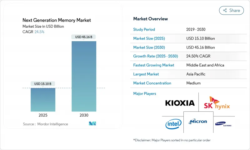
预计下一代记忆体市场将在 2025 年达到 151 亿美元,在 2030 年达到 451.6 亿美元,年复合成长率为 24.5%。
人工智慧训练丛集、边缘伺服器和自动驾驶汽车都面临传统DRAM-NAND架构的延迟限制,这加速了对记忆体的需求。为了弥合日益扩大的运算与记忆体之间的差距,厂商优先发展高频宽架构、持久性储存层级元件和先进封装技术。亚太地区仍是製造强区,而北美晶圆厂则致力于提升并行产能。诸如Compute Express Link (CXL)和Universal Chiplet Interconnect Express (UCIe)等介面创新开始重新定义系统设计理念,推动记忆体池的划分,其扩展能力几乎与加速器的数量呈线性关係。然而,高端製程节点和晶圆供应的限制仍然影响着下一代记忆体市场的定价和分配策略。
全球下一代记忆体市场趋势与洞察
AI主导的超大规模资料中心对HBM的需求
变压器架构的爆炸性成长迫使云端营运商将其伺服器级 DRAM 和固态硬碟预算翻倍,频宽而非容量成为主要瓶颈。高频宽记忆体使链路吞吐量翻倍至 1.5 TB/s 以上,并显着降低了每位元传输的能耗。 SK 海力士报告称,其 2025 年的 HBM 供应已提前售罄,导致全球配额收紧,并促使 2026 年的长期订单预订。美光的观察表明,AI 伺服器的 DRAM 容量将约为传统 x86 节点的两倍。这使得下一代记忆体市场从以位元成本为主导转向以频宽主导,从而为高端定价层级和更高的利润率创造了机会。
汽车L4 ADAS需要即时启动持久内存
L4级自动驾驶要求在断电事件后能够确定性地恢復,并能承受超过150°C的严苛动作温度。铁电存取记忆体(FRAM)装置可在无待机电源的情况下承受10<sup>14</sup>次循环并保持资料完整性,从而确保感测器融合堆迭在冷启动时仍能以高达100GB/s的速率运作。目前,汽车製造商正在评估将FRAM与LPDDR5X垫片结合的非对称持久性非挥发性混合记忆体。这些架构能够保护任务日誌,支援空中升级,并满足ISO 26262的功能安全目标,推动下一代记忆体市场在整个移动出行价值链中的成长。
汽车PCM的热稳定性问题
相变合金在150°C以上的高温下难以维持数据,这会危及部署在沙漠或汽车引擎盖下的事件记录器的完整性。材料工程领域已探索了富锗GeSbTe和串行PCM单元对,将耐久性窗口提升至153°C,但这增加了光刻步骤和成本。因此,OEM厂商的认证週期减缓了PCM的普及,在满足可靠性目标之前,近期的设计订单已转向FRAM和ReRAM。这项限制正在抑制整体成长,尤其是在下一代记忆体市场的汽车细分领域。
细分市场分析
到2024年,挥发性记忆体将占总收入的85.6%,这主要得益于HBM容量的显着溢价。随着AI加速器效能逐渐饱和至1TB/s以下,HBM的采购承诺将跨越多个财年,因此这项优势依然存在。下一代易失性记忆体市场规模预计将继续扩大,但随着ReRAM、PCM和MRAM在边缘运算和计量工作负载中日益普及,其市场份额将会下降。 ReRAM引领非挥发性记忆体的发展势头,凭藉其简单的金属-氧化物堆迭结构,无需额外掩模即可在28nm节点上进行共製造,其复合年增长率高达38.3%。 PCM的热稳定性不断提升,一旦通过10年150°C保持率的认证,预计将推动其在汽车产业的应用。 MRAM的进步与未来EUV微影技术的产能提升和製程简化密切相关,这将缩小其相对于NAND快闪记忆体的每位元溢价。
在架构方面,易失性记忆体製造商目前正在探索堆迭式晶片拓扑结构,以减少晶粒面积并分散产量比率风险。非挥发性记忆体的挑战则透过交叉点阵列和无选择器设计来解决,这些设计无需使用占用面积较大的电晶体。虽然随着ReRAM和PCM供应加速,预计在预测期内挥发性记忆体的市占率将下降约10个百分点,但随着人工智慧伺服器总面积管理记忆体(TAM)翻番,易失性记忆体的绝对收入将会增加。设计人员将继续整合晶粒和非挥发性晶粒,从而形成兼顾耐久性和可持续性的混合堆迭结构。这些动态将确保多节点蓝图的实施,并扩大下一代记忆体市场解决方案的多样性。
在单晶片硅技术出现之前,这种介面已经适应了对频宽频宽极高的加速器。 2024年,DDR和LPDDR通道的市占率维持在38.3%,但每个插槽最多只能支援四个通道。透过PCIe 5.0实现CXL的连贯一致性连线缓解了这个限制,将Terabyte记忆体汇集到一个共用交换器后,并减少了单一记忆体的容量。 2024年8月发布的UCie 2.0规范提供了3D堆迭晶片,其频宽晶粒前几代产品的75倍,使得超大规模资料中心能够在单一HBM堆迭上部署数十个运算晶粒。
展望未来,到2025年,50%的新型高效能运算(HPC)晶片流片将采用2.5D或3D晶片晶粒技术,CXL或UCIe将成为必备设计元素而非可选元素。重定时中心和重定时器将成为新的利润来源。与这些转变同步,PCIe/NVMe将继续逐步实现世代更替,而SATA将逐渐退出市场,成为一种过时的介面。总体而言,新的介面将推动模组化设计的应用,使容量规划与CPU升级週期脱钩,并为下一代记忆体市场的多元化发展提供更多选择。
下一代记忆体市场按技术(易失性、非挥发性)、记忆体介面(DDR/LPDDR、PCIe/NVMe、SATA、其他(CXL、Ucie))、终端设备(消费性电子产品、企业储存和资料中心、汽车电子和ADAS、其他)、晶圆尺寸(200毫米以下、300毫米、450毫米和ADAS、其他)、晶圆尺寸(200毫米以下、300毫米、450毫米和美国地区细分(北美欧洲地区和美国地区)。
区域分析
亚太地区持续保持领先地位,预计2024年营收成长率将达到47.3%,三星、SK海力士和台积电等公司在下一代製程节点上的总合总额将超过850亿美元。中国凭藉国家补贴和优惠融资政策,将国内DRAM产能提升至全球市场份额的5%,併计划于2025年达到10%。日本延长了补贴政策,以维持其本土NAND快闪记忆体生产和专用设备丛集。印度推出了一项製造业激励计划,旨在吸引合资企业参与组装、测试以及最终的3D NAND切片技术。这种区域深度布局确保了供应安全,并促进了下一代记忆体市场的规模化利用。
北美晶片奖励(CHIPS) 促进了美光公司位于爱达荷州的 HBM 晶圆厂和德克萨斯的记忆体组装中心的发展,从而保障了国内国防和超大规模采购所需的产能。墨西哥则确保了后端组装流程,与美国的前端晶圆生产形成互补。加拿大研究机构为超低功耗非挥发性材料的材料科学突破做出了贡献,扩大了北美大陆的研发影响力。
欧洲在《半导体法》的指导下追求战略自主,目标是到2030年占据20%的全球市场份额。德国津贴了一个汽车级记忆体联盟,法国投资了一条ReRAM试点生产线,英国优先发展与晶圆晶粒晶粒的晶片级晶片互连技术智慧财产权。欧盟寻求加强汽车製造商与本地记忆体厂商之间的合作,以增强下一代记忆体市场的区域需求。
中东和非洲的成长速度最快,预计年复合成长率将达到31.2%,这主要得益于沙乌地阿拉伯和阿联酋主权财富基金支持的工厂。土耳其将自身定位为欧亚大陆的封装中心,而南非则利用不断增长的通讯密度来推动消费者对记忆体的需求。儘管基数不大,但积极的资本投入和劳动力技能提升表明,该地区下一代记忆体的市场份额将继续增长。
其他福利:
- Excel格式的市场预测(ME)表
- 3个月的分析师支持
目录
第一章 引言
- 研究假设和市场定义
- 调查范围
第二章调查方法
第三章执行摘要
第四章 市场情势
- 市场概览
- 市场驱动因素
- 人工智慧主导的超大规模资料中心对高频宽记忆体的需求
- 汽车L4 ADAS中对即时开启持久记忆体的需求
- 智慧型手机转换到LPDDR5X和嵌入式ReRAM
- 国家记忆在地化计划
- 工业边缘物联网需要超低功耗FRAM
- 基于 3D XPoint 的资料隐私主导持久记忆体内
- 市场限制
- 450mm 晶圆延迟限制了 ReRAM 的放大
- 与NAND快闪记忆体相比,MRAM的每位元成本更高。
- 汽车级相变材料热稳定性差
- 28nm 以下 STT-MRAM晶圆代工厂集中度
- 价值链分析
- 监理与技术展望
- 波特五力模型
- 新进入者的威胁
- 买方的议价能力
- 供应商的议价能力
- 替代品的威胁
- 竞争对手之间的竞争
- 新兴储存技术蓝图分析
- 影响市场的宏观经济因素
第五章 市场规模与成长预测
- 透过技术
- 非挥发性
- 相变记忆体(PCM)
- 自旋转移磁随机存取记忆体(STT-MRAM)
- 切换 MRAM
- 阻变式随机存取记忆体(ReRAM)
- 3D XPoint/Optan
- 铁电存取记忆体(FeRAM)
- 奈米随机存取记忆体
- 易挥发的
- 高频宽记忆体(HBM)
- 混合储存立方体(HMC)
- 低功耗 DDR5/LPDDR5X
- 非挥发性
- 透过记忆体介面
- DDR/LPDDR
- PCIe/NVMe
- SATA
- 其他(CXL、UCIe)
- 按最终用途设备
- 消费性电子产品
- 企业储存与资料中心
- 汽车电子和ADAS
- 工业物联网和製造业自动化
- 航太与国防
- 医疗保健和医疗设备
- 其他(智慧卡、穿戴式装置)
- 按晶圆尺寸
- 200毫米或更小
- 300 mm
- 450 mm
- 按地区
- 北美洲
- 美国
- 加拿大
- 墨西哥
- 南美洲
- 巴西
- 阿根廷
- 其他南美洲
- 欧洲
- 德国
- 英国
- 法国
- 其他欧洲地区
- 亚太地区
- 中国
- 日本
- 韩国
- 印度
- 亚太其他地区
- 中东和非洲
- 中东
- 沙乌地阿拉伯
- 阿拉伯聯合大公国
- 土耳其
- 其他中东地区
- 非洲
- 南非
- 奈及利亚
- 其他非洲地区
- 北美洲
第六章 竞争情势
- 市场集中度
- 策略趋势
- 市占率分析
- 公司简介
- Samsung Electronics Co., Ltd.
- SK Hynix Inc.
- Micron Technology, Inc.
- Kioxia Holdings Corporation
- Intel Corporation
- Western Digital Corporation
- Everspin Technologies, Inc.
- Crossbar Inc.
- Avalanche Technology Inc.
- Spin Memory, Inc.
- Nantero Inc.
- Weebit Nano Ltd.
- Renesas Electronics Corporation
- Infineon Technologies AG
- NXP Semiconductors NV
- Changxin Memory Technologies(CXMT)
- Taiwan Semiconductor Manufacturing Co. Ltd.
- GlobalFoundries Inc.
- Winbond Electronics Corporation
- Macronix International Co., Ltd.
- Nanya Technology Corporation
- Advanced Semiconductor Engineering(ASE)Inc.
- Powerchip Semiconductor Manufacturing Corp.
- Yangtze Memory Technologies Co.(YMTC)
- Microchip Technology Inc.
第七章 市场机会与未来展望
The Next Generation Memory market size was valued at USD 15.10 billion in 2025 and is forecast to reach USD 45.16 billion by 2030, reflecting a vigorous 24.5% CAGR.
Demand accelerated as AI training clusters, edge servers, and autonomous vehicles all confronted the latency wall of conventional DRAM-NAND hierarchies. Vendors prioritized high-bandwidth architectures, persistent storage class devices, and advanced packaging to close the widening compute-to-memory gap. Asia-Pacific remained the production powerhouse, while North American fab incentives fostered parallel capacity. Interface innovations such as Compute Express Link (CXL) and Universal Chiplet Interconnect Express (UCIe) have begun to redraw system design philosophies, encouraging disaggregated memory pools that scale almost linearly with accelerator count. Supply constraints for premium nodes and wafers, however, continued to shape pricing and allocation strategies across the Next Generation Memory market.
Global Next Generation Memory Market Trends and Insights
AI-driven demand for HBM in hyperscale data centres
Surging transformer model sizes forced cloud operators to double server-level DRAM and solid-state budgets, making bandwidth rather than capacity the primary bottleneck. High Bandwidth Memory multiplied link throughput beyond 1.5 TB/s and delivered dramatic energy savings per bit moved. Global allocation tightened when SK Hynix reported its entire 2025 HBM output sold in advance, which prompted long-term volume reservations for 2026. Micron observed that an AI server deploys nearly twice the DRAM of a classic x86 node. The Next Generation Memory market, therefore, pivoted from bit-cost leadership toward bandwidth leadership, creating premium pricing tiers and margin expansion opportunities.
Automotive L4 ADAS needs instant-on persistent memory
Level 4 autonomy demands deterministic recovery after power events and harsh operating temperatures beyond 150 °C. Ferroelectric RAM devices withstand 1014 cycles while retaining data without standby power, ensuring cold-start availability for sensor fusion stacks that generate up to 100 GB/s. Automakers now evaluate asymmetric persistent-volatile hybrids combining FRAM with LPDDR5X scratch pads. These architectures protect mission logs, facilitate over-the-air updates, and support functional safety goals under ISO 26262, reinforcing growth in the Next Generation Memory market across the mobility value chain.
Thermal stability failures of automotive-grade PCM
Phase-change alloys struggled to retain data above 150 °C, jeopardizing event recorder integrity in desert and under-hood deployments. Material engineering explored Ge-rich GeSbTe and serial PCM cell pairs that push endurance windows to 153 °C but add lithography steps and cost. OEM qualification cycles, therefore, slowed PCM adoption, shifting near-term design wins to FRAM and ReRAM until reliability goals are met. The constraint compressed overall growth, particularly within the automotive subset of the Next Generation Memory market.
Other drivers and restraints analyzed in the detailed report include:
- Smartphone migration to LPDDR5X and embedded ReRAM
- National memory localization programs
- Foundry concentration for sub-28 nm STT-MRAM
For complete list of drivers and restraints, kindly check the Table Of Contents.
Segment Analysis
Volatile devices delivered 85.6% of 2024 revenue, anchored by HBM's steep capacity premiums. That dominance has persisted because AI accelerators saturate anything below 1 TB/s, ensuring HBM purchase commitments stretch multiple fiscal years. The Next Generation Memory market size for volatile solutions is projected to keep expanding in absolute terms even while share slips, as ReRAM, PCM, and MRAM gain credibility in edge and instrumentation workloads. ReRAM leads non-volatile momentum, growing at 38.3% CAGR thanks to simple metal-oxide stacks that co-fabricate on 28 nm nodes without extra masks. PCM's gradual thermal-stability gains are expected to unlock automotive attach once the 10-year, 150 °C retention benchmark is certified. MRAM advances remain tied to future EUV capacity and to process simplification that narrows the per-bit premium versus NAND.
Structurally, volatile makers now explore stacked chiplet topologies, trimming die area, and spreading yield risk. Non-volatile challengers respond with cross-point arrays and selector-less designs that eliminate area-consuming transistors. Over the outlook period, supply acceleration for ReRAM and PCM is expected to erode volatile share by roughly 10 percentage points, although absolute volatile revenue still rises because the AI server TAM doubles. Designers will continue to co-package volatile and non-volatile dies, cultivating hybrid stacks that trade endurance for persistence. Those dynamics ensure a multi-node roadmap, widening solution diversity within the Next Generation Memory market.
Interfaces adapted to bandwidth-hungry accelerators long before monolithic silicon could keep pace. In 2024, DDR and LPDDR channels retained a 38.3% share, but adoption ceilings emerged at four channels per socket. CXL's cache-coherent attach over PCIe 5.0 eased that limit, pooling terabytes of memory behind shared switches and slashing stranded capacity. The arrival of the UCIe 2.0 spec in August 2024 delivered 3D-stacked chiplets with 75 X the prior inter-die bandwidth, empowering hyperscalers to tile dozens of compute dies against a single HBM stack.
Looking ahead, 50% of new HPC tape-outs in 2025 will embed 2.5D or 3D die-to-die links, elevating CXL or UCIe from optional to mandatory design elements. Retiming hubs and retimers emerge as ancillary profit pools. Synchronous to these shifts, PCIe/NVMe continues incremental generational moves, but SATA fades toward archival niches. Collectively, novel interfaces propel modular deployments that decouple capacity planning from CPU upgrade cycles, enlarging diversification options within the Next Generation Memory market.
Next Generation Memory Market is Segmented by Technology (Volatile, and Non-Volatile), by Memory Interface (DDR/LPDDR, PCIe/NVMe, SATA, and Others (CXL, Ucie)), by End-Use Device (Consumer Electronics, Enterprise Storage and Data Centers, Automotive Electronics and ADAS, and More), by Wafer Size (<= 200 Mm, 300 Mm, and 450 Mm), and by Geography (North America, South America, Europe, Asia-Pacific, and Middle East and Africa).
Geography Analysis
Asia-Pacific maintained its leadership with 47.3% revenue in 2024, sustained by Samsung, SK Hynix, and TSMC, whose combined capital plans exceeded USD 85 billion for next-generation nodes. China advanced its indigenous DRAM capacity to a 5% global share and targeted 10% by 2025, guided by state grants and preferential loan terms. Japan's renewed subsidies preserved local NAND output and specialty equipment clusters. India launched fabrication incentive programs that attracted joint ventures geared toward assembly, test, and eventually 3D NAND slicing. This regional depth anchored supply security and fostered volume leverage for the Next Generation Memory market.
North America's CHIPS incentive catalysed Micron's Idaho HBM fab and Texas memory assembly centres, ensuring domestic capacity for defense and hyperscale procurement. Mexico captured backend assembly flows, complementing the United States front-end wafer starts. Canadian institutes contributed materials science breakthroughs aimed at ultra-low-power non-volatiles, expanding the research and development halo of the continent.
Europe pursued strategic autonomy under its semiconductor act, targeting a 20% global share by 2030. Germany funnelled grants toward automotive-grade memory consortia, while France invested in ReRAM pilot lines. The United Kingdom prioritized foundry-agnostic IP for chiplet die-to-die fabrics. Collectively, the bloc sought tighter integration between automotive OEMs and local memory houses, reinforcing regional demand in the Next Generation Memory market.
The Middle East and Africa exhibited the fastest trajectory, with a 31.2% CAGR outlook underpinned by sovereign wealth-fund backed fabs in Saudi Arabia and the UAE. Turkey marketed itself as a Eurasian packaging hub, and South Africa leveraged telecom densification to spur consumer memory uptake. While the base is modest, aggressive capital allocations and labour-force upskilling suggest durable upside for the region's share of the Next Generation Memory market.
- Samsung Electronics Co., Ltd.
- SK Hynix Inc.
- Micron Technology, Inc.
- Kioxia Holdings Corporation
- Intel Corporation
- Western Digital Corporation
- Everspin Technologies, Inc.
- Crossbar Inc.
- Avalanche Technology Inc.
- Spin Memory, Inc.
- Nantero Inc.
- Weebit Nano Ltd.
- Renesas Electronics Corporation
- Infineon Technologies AG
- NXP Semiconductors N.V.
- Changxin Memory Technologies (CXMT)
- Taiwan Semiconductor Manufacturing Co. Ltd.
- GlobalFoundries Inc.
- Winbond Electronics Corporation
- Macronix International Co., Ltd.
- Nanya Technology Corporation
- Advanced Semiconductor Engineering (ASE) Inc.
- Powerchip Semiconductor Manufacturing Corp.
- Yangtze Memory Technologies Co. (YMTC)
- Microchip Technology Inc.
Additional Benefits:
- The market estimate (ME) sheet in Excel format
- 3 months of analyst support
TABLE OF CONTENTS
1 INTRODUCTION
- 1.1 Study Assumptions and Market Definition
- 1.2 Scope of the Study
2 RESEARCH METHODOLOGY
3 EXECUTIVE SUMMARY
4 MARKET LANDSCAPE
- 4.1 Market Overview
- 4.2 Market Drivers
- 4.2.1 AI-Driven Demand for HBM in Hyperscale Data Centers
- 4.2.2 Automotive L4 ADAS Need for Instant-On Persistent Memory
- 4.2.3 Smartphone Migration to LPDDR5X and Embedded ReRAM
- 4.2.4 National Memory Localization Programs
- 4.2.5 Industrial Edge-IoT Requiring Ultra-Low-Power FRAM
- 4.2.6 Data-Privacy-Driven Persistent In-Memory Databases Using 3D XPoint
- 4.3 Market Restraints
- 4.3.1 450 mm Wafer Delay Constraining ReRAM Scale-up
- 4.3.2 High Per-Bit MRAM Cost versus NAND
- 4.3.3 Thermal Stability Failures of Automotive-Grade PCM
- 4.3.4 Foundry Concentration for Sub-28 nm STT-MRAM
- 4.4 Value Chain Analysis
- 4.5 Regulatory and Technological Outlook
- 4.6 Porter's Five Forces
- 4.6.1 Threat of New Entrants
- 4.6.2 Bargaining Power of Buyers
- 4.6.3 Bargaining Power of Suppliers
- 4.6.4 Threat of Substitutes
- 4.6.5 Competitive Rivalry
- 4.7 Emerging Memory Technology Roadmap Analysis
- 4.8 Impact of Macroeconomic factors on the Market
5 MARKET SIZE AND GROWTH FORECASTS (VALUE)
- 5.1 By Technology
- 5.1.1 Non-Volatile
- 5.1.1.1 Phase-Change Memory (PCM)
- 5.1.1.2 Spin-Transfer MRAM (STT-MRAM)
- 5.1.1.3 Toggle MRAM
- 5.1.1.4 Resistive RAM (ReRAM)
- 5.1.1.5 3D XPoint / Optane
- 5.1.1.6 Ferroelectric RAM (FeRAM)
- 5.1.1.7 NanoRAM
- 5.1.2 Volatile
- 5.1.2.1 High-Bandwidth Memory (HBM)
- 5.1.2.2 Hybrid Memory Cube (HMC)
- 5.1.2.3 Low-Power DDR5 / LPDDR5X
- 5.1.1 Non-Volatile
- 5.2 By Memory Interface
- 5.2.1 DDR / LPDDR
- 5.2.2 PCIe / NVMe
- 5.2.3 SATA
- 5.2.4 Others (CXL, UCIe)
- 5.3 By End-Use Device
- 5.3.1 Consumer Electronics
- 5.3.2 Enterprise Storage and Data Centers
- 5.3.3 Automotive Electronics and ADAS
- 5.3.4 Industrial IoT and Manufacturing Automation
- 5.3.5 Aerospace and Defense
- 5.3.6 Healthcare and Medical Devices
- 5.3.7 Others (Smart Cards, Wearables)
- 5.4 By Wafer Size
- 5.4.1 <= 200 mm
- 5.4.2 300 mm
- 5.4.3 450 mm
- 5.5 By Geography
- 5.5.1 North America
- 5.5.1.1 United States
- 5.5.1.2 Canada
- 5.5.1.3 Mexico
- 5.5.2 South America
- 5.5.2.1 Brazil
- 5.5.2.2 Argentina
- 5.5.2.3 Rest of South America
- 5.5.3 Europe
- 5.5.3.1 Germany
- 5.5.3.2 United Kingdom
- 5.5.3.3 France
- 5.5.3.4 Rest of Europe
- 5.5.4 Asia-Pacific
- 5.5.4.1 China
- 5.5.4.2 Japan
- 5.5.4.3 South Korea
- 5.5.4.4 India
- 5.5.4.5 Rest of Asia-Pacific
- 5.5.5 Middle East and Africa
- 5.5.5.1 Middle East
- 5.5.5.1.1 Saudi Arabia
- 5.5.5.1.2 United Arab Emirates
- 5.5.5.1.3 Turkey
- 5.5.5.1.4 Rest of Middle East
- 5.5.5.2 Africa
- 5.5.5.2.1 South Africa
- 5.5.5.2.2 Nigeria
- 5.5.5.2.3 Rest of Africa
- 5.5.1 North America
6 COMPETITIVE LANDSCAPE
- 6.1 Market Concentration
- 6.2 Strategic Moves
- 6.3 Market Share Analysis
- 6.4 Company Profiles {(includes Global level Overview, Market level overview, Core Segments, Financials as available, Strategic Information, Market Rank/Share for key companies, Products and Services, and Recent Developments)}
- 6.4.1 Samsung Electronics Co., Ltd.
- 6.4.2 SK Hynix Inc.
- 6.4.3 Micron Technology, Inc.
- 6.4.4 Kioxia Holdings Corporation
- 6.4.5 Intel Corporation
- 6.4.6 Western Digital Corporation
- 6.4.7 Everspin Technologies, Inc.
- 6.4.8 Crossbar Inc.
- 6.4.9 Avalanche Technology Inc.
- 6.4.10 Spin Memory, Inc.
- 6.4.11 Nantero Inc.
- 6.4.12 Weebit Nano Ltd.
- 6.4.13 Renesas Electronics Corporation
- 6.4.14 Infineon Technologies AG
- 6.4.15 NXP Semiconductors N.V.
- 6.4.16 Changxin Memory Technologies (CXMT)
- 6.4.17 Taiwan Semiconductor Manufacturing Co. Ltd.
- 6.4.18 GlobalFoundries Inc.
- 6.4.19 Winbond Electronics Corporation
- 6.4.20 Macronix International Co., Ltd.
- 6.4.21 Nanya Technology Corporation
- 6.4.22 Advanced Semiconductor Engineering (ASE) Inc.
- 6.4.23 Powerchip Semiconductor Manufacturing Corp.
- 6.4.24 Yangtze Memory Technologies Co. (YMTC)
- 6.4.25 Microchip Technology Inc.
7 MARKET OPPORTUNITIES AND FUTURE OUTLOOK
- 7.1 White-Space and Unmet-Need Assessment
 下一代记忆体市场:按技术、晶圆尺寸、应用和终端用户产业划分-2026-2032年全球市场预测
 下一代记忆体市场规模、份额、趋势和预测:按技术、晶圆尺寸、储存类型、应用和地区划分(2026-2034 年)
 下一代记忆体市场规模、份额和成长分析(按技术、晶圆尺寸、应用和地区划分)—2026-2033年产业预测
 2026-2030年全球记忆体IC市场
 下一代储存技术市场分析及预测(至2035年):按类型、产品类型、技术、应用、组件、形状、材质、装置、最终用户和功能划分
 记忆体IC市场规模、份额及成长分析(按类型、终端用户产业及地区划分)-2026-2033年产业预测
 下一代记忆体市场-2025-2030年预测记忆体IC市场-2025-2030年预测
 全球下一代记忆体技术市场(按技术、垂直行业和地区划分)
 记忆体 IC:市场占有率分析、行业趋势和统计、成长预测(2025-2030 年)