


 |
市场调查报告书
商品编码
1851511
覆晶技术:市场份额分析、行业趋势、统计数据和成长预测(2025-2030 年)Flip Chip Technology - Market Share Analysis, Industry Trends & Statistics, Growth Forecasts (2025 - 2030) |
||||||
※ 本网页内容可能与最新版本有所差异。详细情况请与我们联繫。
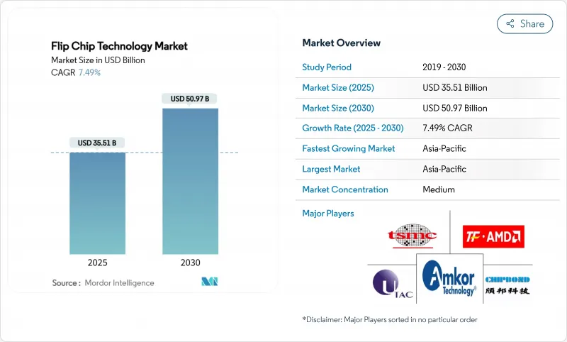
预计到 2025 年,覆晶技术市场规模将达到 355.1 亿美元,到 2030 年将达到 509.7 亿美元,年复合成长率为 7.49%。
这一成长反映了半导体产业向晶片级架构的转型,这种架构需要高密度、散热效率高的互连技术。人工智慧资料中心的建设推动了高频宽记忆体封装技术的发展,铜柱和混合键合线满足了传统焊料凸块无法满足的细间距需求。代工厂纷纷进军封装领域,加速了垂直整合,并对外包组装和测试服务商构成了新的竞争压力。儘管亚太地区保持了规模优势,但北美和欧洲的供应链风险缓解计画促使当地对先进封装设施进行了大量待开发区投资。
全球覆晶技术市场趋势与洞察
对异质整合(人工智慧/高效能运算)的需求快速成长
晶片製造商已从二维微缩转向异构集成,将多个晶片封装在单一封装上,从而推动了对细间距铜-铜互连的需求。台积电计画在2026年将CoWoS产能提升至131万片,显示英伟达等GPU厂商如何塑造了覆晶技术市场。与传统的凸点封装技术相比,这种方法在提高频宽的同时降低了功耗,从而支援了人工智慧加速器的效能蓝图。
铜柱凸点和微凸点互连技术的日益普及
铜柱凸点具有优异的电阻和可靠性,预计在2024年将占据46.3%的市占率。杜邦公司的高速电镀技术实现了均匀的厚度控制,这对于间距小于40µm的晶片至关重要。这一转变削弱了锡铅晶片的主导地位,并为支援覆晶技术市场的3D整合方案铺平了道路。
先进凸块生产线资本密集度高
将间距缩小到10微米以下需要光刻步进机、先进的溅射设备和等离子清洗机,导致每模组生产线成本超过2.5亿美元。台积电在专用封装厂投资900亿美元,凸显了小型竞争对手进入该领域的高门槛。联合研发项目,例如3M参与的美国JOINT联盟,旨在分散整个供应链的风险。
细分市场分析
覆晶覆晶技术市场规模预计将以9.8%的复合年增长率增长。这种混合键合方式已将晶片间距缩小至0.8µm,远超焊料的物理极限。锡铅解决方案仍适用于传统製程节点,而金凸点技术仍主要应用于航太领域。
电镀化学技术的进步使柱体高度均匀性保持在2%以内,这是实现3D堆迭的先决条件。 IEEE的研究表明,在260°C下进行无焊料铜-铜键合是一种可行的异质整合製造方法。技术创新使得铜基材料能够从无铅和贵金属替代品中夺取市场份额。
FC-BGA封装凭藉其在伺服器领域久经考验的可靠性,预计到2024年将占总收入的38.1%。扇出型WLP和麵板级封装预计将达到10.1%的复合年增长率,这主要得益于AI加速器对更大尺寸封装体的需求。日月光(ASE)已拨款2亿美元用于310mm x 310mm面板封装,该封装可提供七倍于传统晶圆的可用面积。随着产量比率线良率的提高,面板级封装中覆晶技术的市场规模也将随之扩大。
CoWoS 和 EMIB 等专用蓝图实现了 HBM 堆迭,这对 AI 训练单元至关重要。 IBM 和英特尔致力于研发玻璃基板,与有机层压板相比,玻璃基板具有更低的翘曲度和更高的线间距比。由于高成本且製程复杂,采用 TSV 技术的 3D IC 在超高频宽元件领域仍处于小众应用,但它们也限制了可实现的效能上限。
覆晶技术市场按晶圆凸点製程(铜柱、锡铅共晶焊料等)、封装技术(FC-BGA、FCCSP/CSP等)、产品(记忆体、CMOS影像感测器等)、终端用户产业(消费性电子和可穿戴设备、汽车和运输、工业和机器人等)以及地区(北美、南美、欧洲、亚太地区细分、中东和机器人等)以及地区(北美、南美、欧洲、亚太地区细分、中东和机器人等)以及地区(北美、南美、欧洲、亚太地区、中东和机器人)进行细分。
区域分析
亚太地区预计到2024年将占总收入的54.5%。该地区拥有绝大多数晶圆厂,并保持着成本优势,因此在覆晶技术市场占据最大份额。政府激励措施支持了下一代晶片的研发,但出口限制促使主要公司在海外建立并行产能。在北美,《晶片法案》(CHIPS Act)加速了晶圆代工和封装产推出的提升,增强了市场韧性并推动了本地需求。随着亚利桑那州和德克萨斯州的园区投入运营,预计北美覆晶技术市场份额将小幅增长。
欧洲透过《欧洲晶片法案》追求技术主权,并将资金投入面板级和玻璃芯基板生产线。 Silicon Box位于诺瓦拉的工厂预计到2028年每周可加工1万块面板,为该地区的生态系统提供支援。中东和非洲仍处于起步阶段,但受益于电子产品最终组装中心对全球供应链的贡献。
供应链多元化将使未来的投资分散到至少三大洲,削弱任何单一地区的统治地位,但亚太地区仍然拥有无与伦比的工程技术深度,并且仍然是大规模製造的中心。
其他福利:
- Excel格式的市场预测(ME)表
- 3个月的分析师支持
目录
第一章 引言
- 研究假设和市场定义
- 调查范围
第二章调查方法
第三章执行摘要
第四章 市场情势
- 市场概览
- 市场驱动因素
- 对异质整合(人工智慧/高效能运算)的需求快速成长
- 铜柱和微凸点互连技术的日益普及
- 穿戴式装置和物联网领域小型化趋势
- 汽车ADAS/电动车的可靠性要求
- 玻璃芯基板的商业测试
- 对晶片级铜-铜混合键结的需求
- 市场限制
- 先进凸块生产线资本密集度高
- 无铅可靠度与翘曲挑战
- 对准产量比率损失小于 10 μm
- 关键金属化学品供应链
- 价值链分析
- 宏观经济因素的影响
- 监管环境
- 技术展望
- 波特五力模型
- 供应商的议价能力
- 买方的议价能力
- 新进入者的威胁
- 替代品的威胁
- 竞争对手之间的竞争
- 投资分析
第五章 市场规模与成长预测
- 透过晶圆凸块工艺
- 铜柱
- 锡铅共晶焊料
- 无铅焊料(锡银焊料、SAC焊料等)
- 金耳环碰撞
- 铜/铜混合/直接键合
- 透过包装技术
- FC-BGA(2D/2.1D/2.5D/3D)
- FCCSP/CSP
- CoWoS/InFO/EMIB
- 扇出 WLP/PLP
- 采用TSV的3D积体电路
- 副产品
- 记忆体(DRAM、HBM)
- CMOS影像感测器
- LED 和迷你/微型 LED
- SoC/应用处理器
- GPU/AI加速器
- CPU/伺服器处理器
- 按最终用途行业划分
- 消费性电子产品和穿戴式装置
- 汽车与运输
- 工业机器人
- 通讯和5G基础设施
- 资料中心和云
- 军事/航太
- 医疗和保健设备
- 按地区
- 北美洲
- 美国
- 加拿大
- 墨西哥
- 南美洲
- 巴西
- 其他南美洲
- 欧洲
- 德国
- 法国
- 英国
- 俄罗斯
- 其他欧洲地区
- 亚太地区
- 中国
- 台湾
- 韩国
- 日本
- 马来西亚
- 新加坡
- 亚太其他地区
- 中东和非洲
- 中东
- 土耳其
- 其他中东地区
- 非洲
- 南非
- 其他非洲地区
- 北美洲
第六章 竞争情势
- 市场集中度
- 策略性倡议(併购、合资、产能扩张)
- 市占率分析
- 公司简介
- Amkor Technology, Inc.
- ASE Technology Holding Co., Ltd.
- Taiwan Semiconductor Manufacturing Company Limited
- Jiangsu Changjiang Electronics Technology Co., Ltd.
- Powertech Technology Inc.
- Chipbond Technology Corporation
- UTAC Holdings Ltd.
- TF-AMD Microelectronics Sdn. Bhd.
- Shinko Electric Industries Co., Ltd.
- Unisem(M)Berhad
- Hana Micron Inc.
- Nepes Corporation
- Carsem(M)Sdn. Bhd.
- Sigurd Microelectronics Corporation
- AT&S Austria Technologie & Systemtechnik AG
- Intel Corporation
- Samsung Electronics Co., Ltd.
- Advanced Micro Devices, Inc.
- Texas Instruments Incorporated
- United Microelectronics Corporation
- STATS ChipPAC Pte. Ltd.
- SFA Semicon Co., Ltd.
- Tongfu Microelectronics Co., Ltd.
- Huatian Technology Co., Ltd.
- Lingsen Precision Industries, Ltd.
第七章 市场机会与未来展望
The flip chip technology market size stood at USD 35.51 billion in 2025 and is on track to reach USD 50.97 billion by 2030, reflecting a 7.49% CAGR.
Growth mirrored the semiconductor industry's transition to chiplet-based architectures that required dense, thermally efficient interconnects. AI data-center build-outs pushed high-bandwidth memory packaging to the fore, while copper-pillar and hybrid bonding lines addressed the fine-pitch needs that traditional solder bumps could not meet. Foundries entered the packaging arena, accelerating vertical integration and bringing new competitive pressures on outsourced assembly and test providers. Asia-Pacific retained scale advantages, yet supply-chain de-risking programs in North America and Europe triggered large green-field investments in advanced packaging facilities.
Global Flip Chip Technology Market Trends and Insights
Surge in Heterogeneous Integration Demand (AI/HPC)
Chipmakers pivoted from 2D scaling to heterogeneous integration that joined multiple chiplets in a single package, lifting demand for fine-pitch Cu-to-Cu interconnects. TSMC's plan to boost CoWoS capacity to 1.31 million units by 2026 illustrated how GPU vendors such as Nvidia shaped the flip chip technology market. The approach enhanced bandwidth while lowering power compared with legacy bumps, supporting the performance roadmap for AI accelerators.
Rising Adoption of Copper-Pillar and Micro-Bump Interconnects
Copper-pillar bumps delivered superior electrical resistance and reliability, explaining their 46.3% 2024 revenue share. High-speed plating chemistries from DuPont provided uniform thickness control essential for sub-40 µm pitches. The shift eroded tin-lead dominance and paved the way for 3D integration schemes that underpin the flip chip technology market.
High Capital Intensity of Advanced Bumping Lines
Scaling to sub-10 µm pitches required lithography steppers, advanced sputter tools, and plasma cleaners that pushed line cost above USD 250 million per module. TSMC earmarked USD 90 billion for dedicated packaging plants, underscoring the entry hurdle for smaller competitors. Collaborative R&D programs such as 3M's participation in the US-JOINT consortium aimed to spread risk across the supply chain.
Other drivers and restraints analyzed in the detailed report include:
- Wearables and IoT Miniaturization Push
- Automotive ADAS/EV Reliability Requirements
- Lead-Free Reliability and Warpage Challenges
For complete list of drivers and restraints, kindly check the Table Of Contents.
Segment Analysis
Copper pillar technology held 46.3% revenue in 2024 within the flip chip technology market. The segment benefited from reduced resistance and heightened current-carrying capability. The flip chip technology market size for Cu-to-Cu hybrid bonding is projected to expand at a 9.8% CAGR as chiplet adoption grows. The hybrid method lowered inter-chip spacing to 0.8 µm, far beyond solder's physical limits. Tin-lead solutions still served legacy nodes, whereas gold-stud bumps remained confined to aerospace.
Advances in electroplated chemistries sustained pillar height uniformity below 2%, a prerequisite for 3D stacks. IEEE research validated solder-free Cu-Cu bonding at 260 °C as a manufacturable path for heterogeneous integration. Innovations positioned copper formats to absorb share from both lead-free and precious-metal alternatives.
FC-BGA commanded 38.1% of 2024 revenue thanks to proven reliability in servers. Fan-out WLP and panel-level formats are expected to record a 10.1% CAGR, catalyzed by AI accelerators demanding large body sizes. ASE allocated USD 200 million to 310 mm X 310 mm panels that promise sevenfold usable area over wafers, a cost breakthrough. The flip chip technology market size for panel-level packages will climb as line yields improve.
Specialty flows such as CoWoS and EMIB enable HBM stacking essential for AI training units. IBM and Intel pursued glass-substrate roadmaps that offer lower warpage and higher line-space ratios than organic laminates. 3D IC with TSV remained a niche for extreme bandwidth-class devices due to high cost and process complexity, but set the ceiling on attainable performance.
Flip Chip Technology Market is Segmented by Wafer Bumping Process (Copper Pillar, Tin-Lead Eutectic Solder, and More), Packaging Technology (FC-BGA, FCCSP/CSP, and More), Product (Memory, CMOS Image Sensor, and More), End-Use Industry (Consumer Electronics and Wearables, Automotive and Transportation, Industrial and Robotics, and More), and Geography (North America, South America, Europe, Asia-Pacific, and Middle East and Africa).
Geography Analysis
Asia-Pacific held 54.5% of 2024 revenue. The region housed the bulk of wafer fabs and retained cost advantages, sustaining the largest slice of the flip chip technology market. Government incentives supported next-node R&D, yet export-control actions induced leading firms to build parallel capacity offshore. North America accelerated foundry and packaging startups under the CHIPS Act, adding resilience and creating a local demand pull. The flip chip technology market share for North America is expected to rise modestly as Arizona and Texas campuses come online.
Europe pursued technology sovereignty through the European Chips Act and directed capital toward panel-level and glass-core substrate lines. Silicon Box's Novara facility is slated to process 10,000 panels weekly by 2028, anchoring a regional ecosystem. Middle East and Africa remained early-stage but benefited from electronics final-assembly hubs that feed into global supply chains.
Supply-chain diversification scattered future investments across at least three continents, muting single-region dominance. However, Asia-Pacific still boasted unmatched engineering depth, keeping it the reference center for high-volume manufacturing.
- Amkor Technology, Inc.
- ASE Technology Holding Co., Ltd.
- Taiwan Semiconductor Manufacturing Company Limited
- Jiangsu Changjiang Electronics Technology Co., Ltd.
- Powertech Technology Inc.
- Chipbond Technology Corporation
- UTAC Holdings Ltd.
- TF-AMD Microelectronics Sdn. Bhd.
- Shinko Electric Industries Co., Ltd.
- Unisem (M) Berhad
- Hana Micron Inc.
- Nepes Corporation
- Carsem (M) Sdn. Bhd.
- Sigurd Microelectronics Corporation
- AT&S Austria Technologie & Systemtechnik AG
- Intel Corporation
- Samsung Electronics Co., Ltd.
- Advanced Micro Devices, Inc.
- Texas Instruments Incorporated
- United Microelectronics Corporation
- STATS ChipPAC Pte. Ltd.
- SFA Semicon Co., Ltd.
- Tongfu Microelectronics Co., Ltd.
- Huatian Technology Co., Ltd.
- Lingsen Precision Industries, Ltd.
Additional Benefits:
- The market estimate (ME) sheet in Excel format
- 3 months of analyst support
TABLE OF CONTENTS
1 INTRODUCTION
- 1.1 Study Assumptions and Market Definition
- 1.2 Scope of the Study
2 RESEARCH METHODOLOGY
3 EXECUTIVE SUMMARY
4 MARKET LANDSCAPE
- 4.1 Market Overview
- 4.2 Market Drivers
- 4.2.1 Surge in heterogeneous integration demand (AI/ HPC)
- 4.2.2 Rising adoption of copper-pillar and micro-bump interconnects
- 4.2.3 Wearables and IoT miniaturization push
- 4.2.4 Automotive ADAS/EV reliability requirements
- 4.2.5 Glass-core substrate commercial trials
- 4.2.6 Demand for chip-let-ready Cu-to-Cu hybrid bonding
- 4.3 Market Restraints
- 4.3.1 High capital intensity of advanced bumping lines
- 4.3.2 Lead-free reliability and warpage challenges
- 4.3.3 Sub-10 µm alignment yield losses
- 4.3.4 Supply-chain exposure to critical metal chemicals
- 4.4 Value Chain Analysis
- 4.5 Impact of Macroeconomic Factors
- 4.6 Regulatory Landscape
- 4.7 Technological Outlook
- 4.8 Porter's Five Forces
- 4.8.1 Bargaining Power of Suppliers
- 4.8.2 Bargaining Power of Buyers
- 4.8.3 Threat of New Entrants
- 4.8.4 Threat of Substitutes
- 4.8.5 Intensity of Competitive Rivalry
- 4.9 Investment Analysis
5 MARKET SIZE AND GROWTH FORECASTS (VALUE)
- 5.1 By Wafer Bumping Process
- 5.1.1 Copper Pillar
- 5.1.2 Tin-Lead Eutectic Solder
- 5.1.3 Lead-Free Solder (SnAg, SAC, etc.)
- 5.1.4 Gold-Stud Bumping
- 5.1.5 Cu-to-Cu Hybrid / Direct Bond
- 5.2 By Packaging Technology
- 5.2.1 FC-BGA (2D/2.1D/2.5D/3D)
- 5.2.2 FCCSP / CSP
- 5.2.3 CoWoS / InFO / EMIB
- 5.2.4 Fan-Out WLP / PLP
- 5.2.5 3D IC with TSV
- 5.3 By Product
- 5.3.1 Memory (DRAM, HBM)
- 5.3.2 CMOS Image Sensor
- 5.3.3 LED and Mini/Micro-LED
- 5.3.4 SoC / Application Processor
- 5.3.5 GPU / AI Accelerator
- 5.3.6 CPU / Server Processor
- 5.4 By End-Use Industry
- 5.4.1 Consumer Electronics and Wearables
- 5.4.2 Automotive and Transportation
- 5.4.3 Industrial and Robotics
- 5.4.4 Telecommunications and 5G Infrastructure
- 5.4.5 Data Center and Cloud
- 5.4.6 Military and Aerospace
- 5.4.7 Medical and Healthcare Devices
- 5.5 By Geography
- 5.5.1 North America
- 5.5.1.1 United States
- 5.5.1.2 Canada
- 5.5.1.3 Mexico
- 5.5.2 South America
- 5.5.2.1 Brazil
- 5.5.2.2 Rest of South America
- 5.5.3 Europe
- 5.5.3.1 Germany
- 5.5.3.2 France
- 5.5.3.3 United Kingdom
- 5.5.3.4 Russia
- 5.5.3.5 Rest of Europe
- 5.5.4 Asia-Pacific
- 5.5.4.1 China
- 5.5.4.2 Taiwan
- 5.5.4.3 South Korea
- 5.5.4.4 Japan
- 5.5.4.5 Malaysia
- 5.5.4.6 Singapore
- 5.5.4.7 Rest of Asia-Pacific
- 5.5.5 Middle East and Africa
- 5.5.5.1 Middle East
- 5.5.5.1.1 Turkey
- 5.5.5.1.2 Rest of Middle East
- 5.5.5.2 Africa
- 5.5.5.2.1 South Africa
- 5.5.5.2.2 Rest of Africa
- 5.5.1 North America
6 COMPETITIVE LANDSCAPE
- 6.1 Market Concentration
- 6.2 Strategic Moves (M&A, JV, Capacity Expansions)
- 6.3 Market Share Analysis
- 6.4 Company Profiles (includes Global-level Overview, Market-level Overview, Core Segments, Financials, Strategic Information, Market Rank/Share, Products and Services, Recent Developments)
- 6.4.1 Amkor Technology, Inc.
- 6.4.2 ASE Technology Holding Co., Ltd.
- 6.4.3 Taiwan Semiconductor Manufacturing Company Limited
- 6.4.4 Jiangsu Changjiang Electronics Technology Co., Ltd.
- 6.4.5 Powertech Technology Inc.
- 6.4.6 Chipbond Technology Corporation
- 6.4.7 UTAC Holdings Ltd.
- 6.4.8 TF-AMD Microelectronics Sdn. Bhd.
- 6.4.9 Shinko Electric Industries Co., Ltd.
- 6.4.10 Unisem (M) Berhad
- 6.4.11 Hana Micron Inc.
- 6.4.12 Nepes Corporation
- 6.4.13 Carsem (M) Sdn. Bhd.
- 6.4.14 Sigurd Microelectronics Corporation
- 6.4.15 AT&S Austria Technologie & Systemtechnik AG
- 6.4.16 Intel Corporation
- 6.4.17 Samsung Electronics Co., Ltd.
- 6.4.18 Advanced Micro Devices, Inc.
- 6.4.19 Texas Instruments Incorporated
- 6.4.20 United Microelectronics Corporation
- 6.4.21 STATS ChipPAC Pte. Ltd.
- 6.4.22 SFA Semicon Co., Ltd.
- 6.4.23 Tongfu Microelectronics Co., Ltd.
- 6.4.24 Huatian Technology Co., Ltd.
- 6.4.25 Lingsen Precision Industries, Ltd.
7 MARKET OPPORTUNITIES AND FUTURE OUTLOOK
- 7.1 White-space and Unmet-Need Assessment
 全球覆晶市场:依凸点类型、封装技术、终端应用产业、国家及地区划分-产业分析、市场规模、份额及预测(2025-2032年)
 覆晶市场分析及预测(至2035年):依类型、产品类型、服务、技术、组件、应用、材料类型、製程、最终用户、设备划分
 全球覆晶市场规模、份额、趋势和成长分析报告(2026-2034)
 倒装晶片/WLP製造与市场分析
 2026年全球覆晶市场报告倒装晶片市场规模、占有率、成长及全球产业分析:依类型、应用和地区划分的洞察与预测(2026-2034)
 覆晶BGA市场按产品类型、焊球数量、基板材料、装置类型、分销管道和应用划分-2026-2032年全球预测
 倒装晶片市场-全球产业规模、份额、趋势、机会和预测,按晶圆凸点製程、封装技术(BGA 和 CSP)、产品、最终用户、地区和竞争格局划分,2021-2031 年预测
 覆晶市场规模、份额和成长分析(按封装类型、封装技术、凸点技术、最终用途和地区划分)-2026-2033年产业预测覆晶技术市场-2025-2030年预测