


 |
市场调查报告书
商品编码
1851742
半导体材料:市场份额分析、行业趋势、统计数据和成长预测(2025-2030 年)Semiconductor Materials - Market Share Analysis, Industry Trends & Statistics, Growth Forecasts (2025 - 2030) |
||||||
※ 本网页内容可能与最新版本有所差异。详细情况请与我们联繫。
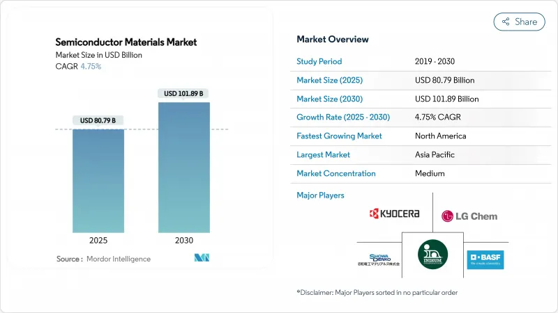
预计到 2025 年,半导体材料市场规模将达到 807.9 亿美元,到 2030 年将扩大到 1,018.9 亿美元,预测期内复合年增长率为 4.75%。
人工智慧优化架构的持续发展和车辆电气化正将传统硅材料推向物理极限,并重塑材料需求。随着晶片设计和3D堆迭架构对互连和散热解决方案的需求日益增长,先进封装材料正以11.8%的复合年增长率加速成长。儘管製造材料仍占据主导地位,预计到2024年将占收入份额的63%,但价值创造正在向下游转移,封装创新正在影响系统性能。电动车对宽能带隙功率元件的需求成长,以及北美和欧洲国内材料供应链因战略性回流计画而奖励,也推动了需求成长。围绕关键化学品的地缘政治紧张局势(最显着的例子是日本在2019年对氟化氢的限制)凸显了多元化筹资策略的重要性。
全球半导体材料市场趋势与洞察
数位化主导的晶圆厂扩张
到2027年,300毫米晶圆厂产能计画投资4,000亿美元,将是半导体史上规模最大的产能扩张。光是德克萨斯一家就在美国七座晶圆厂投资600亿美元,而美光科技计画在国内记忆体工厂投资2,000亿美元。先进晶圆厂每片晶圆消费量的特种化学品比上一代晶圆厂多40%,迫使供应商在多个地区扩大超高纯度化学品的生产。
5G/AI终端设备的普及
人工智慧加速器推动了前所未有的频宽和散热极限,导致每个封装晶片的材料成本是传统处理器的三倍。 HBM堆迭结构依赖硅通孔铜柱和超薄晶片黏接膜,需要富含银的配方。FUJIFILM的目标是到2030年实现5,000亿日圆的半导体材料销售额,主要驱动力是专为人工智慧节点量身打造的EUV光阻剂。在汽车领域,LG化学用于SiC功率模组的高性能银胶表明,人工智慧主导的移动性将如何提高对温度和电压的要求。
消费性电子产品的循环经济
预计半导体封装材料市场在2023年将下滑15.5%,随后在2024年復苏,显示智慧型手机和个人电脑市场的放缓将迅速波及化学品需求。高达30%的季度库存波动将给专注于大批量消费品的供应商带来压力。多元化发展至汽车、工业和基础设施领域可以缓解但无法消除这种波动。人工智慧增强型消费设备的出现可能会降低週期性波动幅度,但同时也带来新的预测复杂性,因为材料成本上涨将取代销售成长成为主要的收入驱动因素。
细分市场分析
晶圆製造材料,由于每片晶圆需要数百道蚀刻、沉积和平坦化工序,预计到2024年将占半导体材料市场收入的63%。湿式化学品、电子气体和化学机械抛光(CMP)耗材是最大的成本组成部分。以以金额为准,到2024年,这部分半导体材料市场的价值将超过500亿美元。先进封装目前规模较小,但随着晶片分离技术的进步,金属化密度和热界面性能将超越有机层压材料的能力,其市场将以9.2%的复合年增长率成长。因此,半导体材料市场正朝着晶粒晶片架构设计的基板、底部填充材料和模塑化合物方向发展,而封装原料市场也将以11.8%的复合年增长率成长。
这一转变也重塑了产业格局。製造供应商将享受规模经济效益,但成长曲线将更加平缓。例如,基于BT树脂的基板能够实现比传统FR-4更精细的线条和间距,从而提升AI加速器的性能。材料供应商,无论采用何种製程节点和封装架构,都能透过在晶圆製造初期和模组最终阶段分别控製成本,从而获得跨週期的竞争力。
由于湿式製程化学品在清洗、剥离和蚀刻等製程中发挥普遍作用,它们仍将是最大的材料类别,预计到2024年将占总支出的24%。随着製程节点的推进,化学品用量也在增加,最先进的晶圆厂每片晶圆所使用的酸和碱比28nm製程线多40%。包括氟化氢和三氟化氮在内的特种气体面临地缘政治供应限制。日本2019年的出口限制导致韩国的氟化氢出货量减少了96.8%,促使韩国转向台湾、比利时和美国地采购。
随着製程尺寸的不断缩小,平坦化步骤也随之增加,CMP 浆料和垫片的需求量稳定上升。光阻剂随着 EUV 技术的普及而不断发展,新型聚合物平台必须能够承受 13.5nm 的光子曝光,同时劣化线边缘粗糙度。基板技术的创新也从 300mm 硅扩展到用于功率元件的高品质 SiC 晶锭和 200mm GaN 晶圆。总而言之,这些变化正在再形成半导体材料市场,迫使供应商在纯度、永续性和成本之间寻求平衡。
半导体材料市场按应用(製造、封装)、材料类型(晶圆基板、特殊材料、其他)、终端用户产业(消费电子、通讯、其他)、技术节点、晶圆厂所有权(整合元件製造商、纯晶圆厂、其他)和地区进行细分。市场预测以美元计价。
区域分析
亚太地区预计到2024年将占全球销售额的55%,主要得益于台湾、韩国、日本和中国当地密集的製造业生态系统。然而,这种区域集中也使得供应链更容易受到出口管制衝击,2019年的氢氟酸事件就印证了这一点。日本供应商正透过投资5.45亿美元新创工厂和进行收购来增强自身抵御风险的能力,以确保对高纯度生产线的本地化控制。
北美是成长最快的地区,在《晶片法案》(CHIPS Act)520亿美元激励措施的推动下,预计到2030年将实现6.4%的复合年增长率。英特尔、台积电和三星正在建造年产能超过2,000万片的晶圆,这得益于液化空气集团(在爱达荷州投资2.5亿美元)和恩特格里斯(在科罗拉多斯普林斯投资7,500万美元)的同步投资。国内封装和测试的扩张正在缩短前置作业时间,并刺激对本地生产的焊球合金和先进基板的需求。同时,环境监管机构正在加速推广无PFAS化学品,这为本地创新者提供了立足之地。
欧洲正利用晶片製造工艺,力争2030年占据全球20%的市场。默克、BASF和林德正在升级其超纯硫酸和氨生产线,以支援德国和法国的新工厂。印度正崛起为成熟的节点和辅助OSAT(外包半导体加工)中心,吸引特种气体生产商进行待开发区投资。中东和非洲仍在发展中,但预计将受益于各国为可再生能源计划相关的电力设备组装采取的本土化措施。总而言之,这些措施将从地理上重新分配半导体材料市场,在降低地缘政治风险的同时,透过冗余增加总支出。
其他福利:
- Excel格式的市场预测(ME)表
- 3个月的分析师支持
目录
第一章 引言
- 研究假设和市场定义
- 调查范围
第二章调查方法
第三章执行摘要
第四章 市场情势
- 市场概览
- 市场驱动因素
- 数位化主导的工厂扩张
- 5G/AI终端设备的普及
- 汽车电气化和高级驾驶辅助系统
- 先进节点投资(5nm)
- 晶片组和异构整合物料清单提升
- 区域化主导的安全库存政策
- 市场限制
- 消费性电子产品的循环经济
- 新化学品的高资本密集度
- 关于 PFAS 化学品的环境法规
- 亚太地区氢氟酸供应安全
- 价值/供应链分析
- 监管环境
- 技术展望
- 波特五力模型
- 供应商的议价能力
- 消费者议价能力
- 新进入者的威胁
- 替代品的威胁
- 竞争对手之间的竞争
第五章 市场规模与成长预测
- 透过使用
- 製造
- 製程化学品
- 光掩模
- 电子气体
- 光阻剂辅助设备
- 溅镀靶
- 硅
- 其他加工材料
- 包装
- 基板
- 导线架
- 陶瓷包装
- 连接线
- 封装树脂
- 晶粒黏接材料
- 其他包装材料
- 製造
- 依材料类型
- 晶圆基板
- 特种气体
- 湿式化学品
- 光阻剂和配件
- CMP浆料和垫片
- 先进包装材料
- 按最终用户行业划分
- 消费性电子产品
- 通讯领域
- 製造/工业IoT
- 车
- 能源与公用事业
- 其他的
- 依技术节点
- 45奈米或以上
- 28-45 nm
- 14-22 nm
- 7-10 nm
- 小于5奈米
- 由 Fab Ownership 提供
- IDM
- 纯粹的选角
- 无晶圆厂(透过代工厂购买材料)
- OSAT/组装和测试
- 按地区
- 北美洲
- 美国
- 加拿大
- 墨西哥
- 欧洲
- 英国
- 德国
- 法国
- 义大利
- 其他欧洲地区
- 亚太地区
- 中国
- 日本
- 印度
- 韩国
- 亚太其他地区
- 中东
- 以色列
- 沙乌地阿拉伯
- 阿拉伯聯合大公国
- 土耳其
- 其他中东地区
- 非洲
- 南非
- 埃及
- 其他非洲地区
- 南美洲
- 巴西
- 阿根廷
- 其他南美洲
- 北美洲
第六章 竞争情势
- 市场集中度
- 策略趋势
- 市占率分析
- 公司简介
- DuPont de Nemours, Inc.
- BASF SE
- Showa Denko Materials Co., Ltd.
- Tokyo Ohka Kogyo Co., Ltd.
- Shin-Etsu Chemical Co., Ltd.
- Merck KGaA(EMD Electronics)
- LG Chem Ltd.
- Henkel AG and Co. KGaA
- Indium Corporation
- SUMCO Corporation
- JSR Corporation
- KYOCERA Corporation
- Versum Materials(Merck)
- Caplinq Europe BV
- Nichia Corporation
- International Quantum Epitaxy Plc.
- Sumitomo Chemical Co., Ltd.
- DOW Inc.
- Air Liquide Electronics
- Linde plc Electronics
- SK Materials Co., Ltd.
第七章 市场机会与未来展望
The semiconductor materials market size reached USD 80.79 billion in 2025 and is projected to expand to USD 101.89 billion by 2030, advancing at a 4.75% CAGR during the forecast period.
Continued AI-optimized architectures and automotive electrification are reshaping material requirements as traditional silicon approaches fundamental physics limits. Advanced packaging materials are accelerating at an 11.8% CAGR because chiplet designs and 3D stacking architectures need novel interconnect and thermal solutions. Fabrication materials still dominate with a 63% revenue share in 2024, but value creation is migrating downstream where packaging innovation increasingly shapes system performance. Demand is also buoyed by the pivot to wide-bandgap power devices in electric vehicles and by strategic reshoring programs that incentivize domestic material supply chains in North America and Europe. Geopolitical tensions surrounding critical chemicals-most visibly Japan's 2019 hydrogen-fluoride curbs-have underscored the importance of diversified sourcing strategies.
Global Semiconductor Materials Market Trends and Insights
Digitalization-led Fab Expansions
The USD 400 billion earmarked for 300 mm fab equipment through 2027 represents the largest capacity build-out in semiconductor history. Texas Instruments alone has committed USD 60 billion across seven US fabs, while Micron plans USD 200 billion in domestic memory facilities. . Each advanced fab consumes 40% more specialty chemicals per wafer than the previous generation, intensifying pressure on suppliers to scale ultra-high-purity production in multiple geographies.
5G/AI End-Device Proliferation
AI accelerators push unprecedented bandwidth and thermal envelopes, tripling materials spend per packaged chip relative to conventional processors. HBM stacks rely on through-silicon-via copper pillars and ultra-thin die-attach films that demand silver-rich formulations. Fujifilm has targeted JPY 500 billion in semiconductor-materials revenue by 2030, largely from EUV photoresists tailored for AI-centric nodes. On the automotive side, LG Chem's high-performance silver paste for SiC power modules exemplifies how AI-driven mobility raises both temperature and voltage requirements.
Cyclicality of Consumer Electronics
The semiconductor packaging materials segment fell 15.5% in 2023 before rebounding in 2024, illustrating how smartphone and PC slowdowns ripple quickly through chemical demand. Inventory swings of up to 30% within a quarter pressure suppliers devoted to high-volume consumer lines. Diversification into automotive, industrial and infrastructure is mitigating but not eliminating this volatility. The advent of AI-enhanced consumer devices may lower cyclical amplitude yet introduce fresh forecasting complexity as bill-of-materials inflation replaces unit growth as the primary revenue lever.
Other drivers and restraints analyzed in the detailed report include:
- Automotive Electrification & ADAS
- Advanced-Node Investments (<=5 nm)
- High Capital Intensity for New Chemistries
For complete list of drivers and restraints, kindly check the Table Of Contents.
Segment Analysis
Fabrication materials commanded 63% revenue in 2024, reflecting the hundreds of etch, deposition and planarization steps per wafer. Wet chemicals, electronic gases and CMP consumables form the largest cost pools. In value terms, this slice of the semiconductor materials market size equated to more than USD 50 billion in 2024. Advanced packaging, while smaller today, is scaling at a 9.2% CAGR as chiplet partitioning pushes metallization density and thermal-interface performance beyond organic laminate capabilities. The semiconductor materials market is therefore tilting toward substrates, under-fills and mold compounds engineered for multi-die architectures, supported by an 11.8% CAGR in packaging raw materials.
The pivot also recasts industry power dynamics. Fabrication suppliers benefit from scale but face flatter growth curves, whereas packaging innovators can secure design-in wins with higher long-term elasticity. For instance, BT-resin-based substrates enable finer lines and spaces than traditional FR-4, unlocking performance gains in AI accelerators. Materials vendors that straddle both process nodes and package architectures gain cross-cycle resilience, capturing spend both at wafer start and at module finish.
Wet-process chemicals remained the largest material class, representing 24% of 2024 spend, thanks to their universal role in cleaning, stripping and etching. Ongoing node migration increases dosage intensity-leading-edge fabs use 40% more acids and bases per wafer than 28 nm lines. Specialty gases, including hydrogen fluoride and nitrogen trifluoride, follow closely in value and face geopolitical supply scrutiny. Japan's 2019 export restrictions slashed hydrogen-fluoride shipments to South Korea by 96.8%, prompting rapid dual-sourcing across Taiwan, Belgium and the United States.
CMP slurries and pads show steady upticks as the number of planarization steps rises with each design shrink. Photoresists evolve with EUV adoption; new polymer platforms must endure 13.5 nm photon bombardment without line-edge roughness degradation. Substrate innovation is broadening beyond 300 mm silicon to include high-quality SiC boules and 200 mm GaN wafers for power devices. Collectively, these shifts are reshaping the semiconductor materials market, forcing suppliers to balance purity, sustainability and cost.
Semiconductor Materials Market Segmented by Application (Fabrication, Packaging), Material Type (Wafer Substrates, Specialty and More), End-User Industry (Consumer Electronics, Telecommunications, and More), Technology Node, Fab Ownership (IDM, Pure-Play and More), and Geography. The Market Forecasts are Provided in Terms of Value (USD).
Geography Analysis
Asia-Pacific commanded 55% of 2024 revenue owing to its dense manufacturing ecosystem across Taiwan, South Korea, Japan and mainland China. However, the region's concentration exposes supply chains to export-control shocks as evidenced by the 2019 hydrogen-fluoride episode. Japanese suppliers are fortifying resilience with USD 545 million in new chemical plants and targeted acquisitions to secure local control of high-purity lines.
North America is the fastest-growing territory, advancing at a 6.4% CAGR through 2030 on the back of USD 52 billion in CHIPS Act incentives. Intel, TSMC and Samsung are collectively building more than 20 million wafers per-year of capacity, catalysing parallel investments from Air Liquide (USD 250 million in Idaho) and Entegris (USD 75 million for Colorado Springs). Domestic packaging and test expansions are shortening lead times and stimulating demand for solder-ball alloys and advanced substrates produced within the region. Environmental regulators are simultaneously accelerating adoption of PFAS-free chemistries, giving local innovators a foothold.
Europe is leveraging its Chips Act to reach 20% global share by 2030. Merck, BASF and Linde are upgrading ultra-purity sulfuric and ammonia lines to support new fabs in Germany and France. India is emerging as a secondary hub for mature-node and OSAT work, attracting specialty-gas makers with greenfield investments. The Middle East and Africa remain nascent but could benefit from sovereign efforts to localize power-device assembly tied to renewable energy projects. Collectively these moves are geographically redistributing the semiconductor materials market, increasing total spend through redundancy while easing geopolitical risk.
- DuPont de Nemours, Inc.
- BASF SE
- Showa Denko Materials Co., Ltd.
- Tokyo Ohka Kogyo Co., Ltd.
- Shin-Etsu Chemical Co., Ltd.
- Merck KGaA (EMD Electronics)
- LG Chem Ltd.
- Henkel AG and Co. KGaA
- Indium Corporation
- SUMCO Corporation
- JSR Corporation
- KYOCERA Corporation
- Versum Materials (Merck)
- Caplinq Europe B.V.
- Nichia Corporation
- International Quantum Epitaxy Plc.
- Sumitomo Chemical Co., Ltd.
- DOW Inc.
- Air Liquide Electronics
- Linde plc Electronics
- SK Materials Co., Ltd.
Additional Benefits:
- The market estimate (ME) sheet in Excel format
- 3 months of analyst support
TABLE OF CONTENTS
1 INTRODUCTION
- 1.1 Study Assumptions and Market Definition
- 1.2 Scope of the Study
2 RESEARCH METHODOLOGY
3 EXECUTIVE SUMMARY
4 MARKET LANDSCAPE
- 4.1 Market Overview
- 4.2 Market Drivers
- 4.2.1 Digitalisation-led fab expansions
- 4.2.2 5G/AI end-device proliferation
- 4.2.3 Automotive electrification and ADAS
- 4.2.4 Advanced-node investments (5 nm)
- 4.2.5 Chiplet and heterogenous integration BOM uplift
- 4.2.6 Regionalisation-driven safety-stock policies
- 4.3 Market Restraints
- 4.3.1 Cyclicality of consumer electronics
- 4.3.2 High capital intensity for new chemistries
- 4.3.3 Environmental regulations on PFAS chemistries
- 4.3.4 Hydrogen fluoride supply security in APAC
- 4.4 Value / Supply Chain Analysis
- 4.5 Regulatory Landscape
- 4.6 Technological Outlook
- 4.7 Porter's Five Forces
- 4.7.1 Bargaining Power of Suppliers
- 4.7.2 Bargaining Power of Consumers
- 4.7.3 Threat of New Entrants
- 4.7.4 Threat of Substitutes
- 4.7.5 Intensity of Competitive Rivalry
5 MARKET SIZE AND GROWTH FORECASTS (VALUE)
- 5.1 By Application
- 5.1.1 Fabrication
- 5.1.1.1 Process Chemicals
- 5.1.1.2 Photomasks
- 5.1.1.3 Electronic Gases
- 5.1.1.4 Photoresist Ancillaries
- 5.1.1.5 Sputtering Targets
- 5.1.1.6 Silicon
- 5.1.1.7 Other Fabrication Materials
- 5.1.2 Packaging
- 5.1.2.1 Substrates
- 5.1.2.2 Lead-frames
- 5.1.2.3 Ceramic Packages
- 5.1.2.4 Bonding Wire
- 5.1.2.5 Encapsulation Resins
- 5.1.2.6 Die-Attach Materials
- 5.1.2.7 Other Packaging Materials
- 5.1.1 Fabrication
- 5.2 By Material Type
- 5.2.1 Wafer Substrates
- 5.2.2 Specialty Gases
- 5.2.3 Wet Process Chemicals
- 5.2.4 Photoresists and Ancillaries
- 5.2.5 CMP Slurries and Pads
- 5.2.6 Advanced Packaging Materials
- 5.3 By End-User Industry
- 5.3.1 Consumer Electronics
- 5.3.2 Telecommunications
- 5.3.3 Manufacturing / Industrial IoT
- 5.3.4 Automotive
- 5.3.5 Energy and Utility
- 5.3.6 Others
- 5.4 By Technology Node
- 5.4.1 More than 45 nm
- 5.4.2 28-45 nm
- 5.4.3 14-22 nm
- 5.4.4 7-10 nm
- 5.4.5 Less than 5 nm
- 5.5 By Fab Ownership
- 5.5.1 IDM
- 5.5.2 Pure-play Foundry
- 5.5.3 Fabless (materials purchased via foundry)
- 5.5.4 OSAT / Assembly and Test
- 5.6 By Geography
- 5.6.1 North America
- 5.6.1.1 United States
- 5.6.1.2 Canada
- 5.6.1.3 Mexico
- 5.6.2 Europe
- 5.6.2.1 United Kingdom
- 5.6.2.2 Germany
- 5.6.2.3 France
- 5.6.2.4 Italy
- 5.6.2.5 Rest of Europe
- 5.6.3 Asia-Pacific
- 5.6.3.1 China
- 5.6.3.2 Japan
- 5.6.3.3 India
- 5.6.3.4 South Korea
- 5.6.3.5 Rest of Asia-Pacific
- 5.6.4 Middle East
- 5.6.4.1 Israel
- 5.6.4.2 Saudi Arabia
- 5.6.4.3 United Arab Emirates
- 5.6.4.4 Turkey
- 5.6.4.5 Rest of Middle East
- 5.6.5 Africa
- 5.6.5.1 South Africa
- 5.6.5.2 Egypt
- 5.6.5.3 Rest of Africa
- 5.6.6 South America
- 5.6.6.1 Brazil
- 5.6.6.2 Argentina
- 5.6.6.3 Rest of South America
- 5.6.1 North America
6 COMPETITIVE LANDSCAPE
- 6.1 Market Concentration
- 6.2 Strategic Moves
- 6.3 Market Share Analysis
- 6.4 Company Profiles (includes Global level Overview, Market level overview, Core Segments, Financials as available, Strategic Information, Market Rank/Share for key companies, Products and Services, and Recent Developments)
- 6.4.1 DuPont de Nemours, Inc.
- 6.4.2 BASF SE
- 6.4.3 Showa Denko Materials Co., Ltd.
- 6.4.4 Tokyo Ohka Kogyo Co., Ltd.
- 6.4.5 Shin-Etsu Chemical Co., Ltd.
- 6.4.6 Merck KGaA (EMD Electronics)
- 6.4.7 LG Chem Ltd.
- 6.4.8 Henkel AG and Co. KGaA
- 6.4.9 Indium Corporation
- 6.4.10 SUMCO Corporation
- 6.4.11 JSR Corporation
- 6.4.12 KYOCERA Corporation
- 6.4.13 Versum Materials (Merck)
- 6.4.14 Caplinq Europe B.V.
- 6.4.15 Nichia Corporation
- 6.4.16 International Quantum Epitaxy Plc.
- 6.4.17 Sumitomo Chemical Co., Ltd.
- 6.4.18 DOW Inc.
- 6.4.19 Air Liquide Electronics
- 6.4.20 Linde plc Electronics
- 6.4.21 SK Materials Co., Ltd.
7 MARKET OPPORTUNITIES AND FUTURE OUTLOOK
- 7.1 White-space and Unmet-Need Assessment
 全球先进钻石材料与技术市场(2026-2036)
 半导体用钻石材料市场规模、份额及成长分析(依材料类型、形状、应用、终端用户产业及地区划分)-2026-2033年产业预测
 5G网路可再生半导体材料市场分析及预测(至2035年):类型、产品类型、服务、技术、组件、应用、製程、最终用户、模组、安装类型先进透明半导体市场分析及预测(至2035年):依类型、产品类型、技术、应用、材料类型、装置、最终使用者、功能及安装类型划分可回收半导体材料市场分析及预测(至2035年):类型、产品、服务、技术、应用、材料类型、製程、最终用户、功能、设备基于半导体的氢气分离市场分析及预测(至2035年):按类型、产品类型、技术、应用、材料类型、製程、最终用户、安装类型、设备和功能划分生物可降解半导体奈米复合材料市场分析及预测(至2035年):按类型、产品类型、服务、技术、应用、材料类型、装置、最终用户和功能划分生物基半导体塑胶市场分析及预测(至2035年):类型、产品、技术、应用、材料类型、组件、製程、最终用户、功能、安装类型生物基半导体封装市场分析及预测(至2035年):依类型、产品类型、技术、应用、材料类型、组件类型、最终用户、製程、功能及安装类型划分生物降解电子元件市场分析及预测(至2035年):类型、产品类型、技术、应用、材料类型、製程、最终用户、功能、安装类型