


 |
市场调查报告书
商品编码
1906086
OSAT(外包半导体封装测试)市场:市场份额分析、行业趋势和统计数据、成长预测(2026-2031)Outsourced Semiconductor Assembly And Test (OSAT) - Market Share Analysis, Industry Trends & Statistics, Growth Forecasts (2026 - 2031) |
||||||
※ 本网页内容可能与最新版本有所差异。详细情况请与我们联繫。
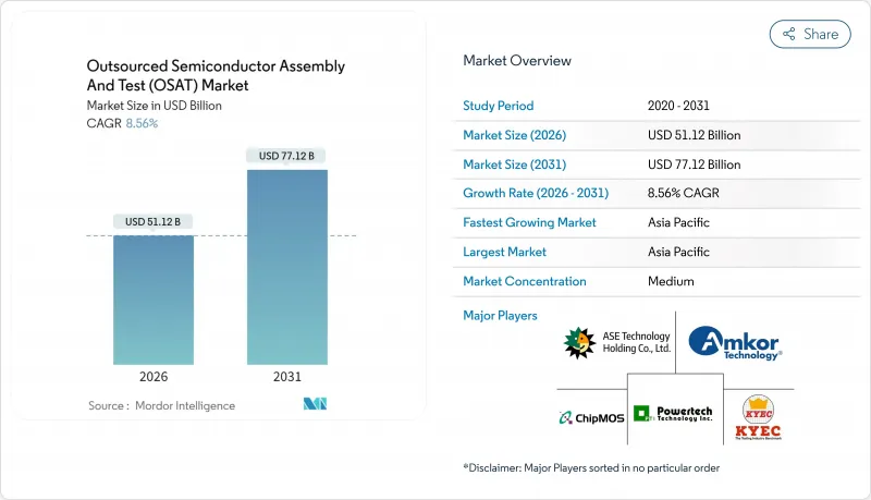
2025 年 OSAT(外包半导体组装和测试)市值为 470.9 亿美元,预计到 2031 年将达到 771.2 亿美元,而 2026 年为 511.2 亿美元。
预计在预测期(2026-2031 年)内,复合年增长率将达到 8.56%。
人工智慧、高效能运算和汽车电气化的持续进步正在推动对先进封装技术和安全关键型测试流程的需求,从而扩大专业后端服务供应商的潜在市场。亚太地区的供应商凭藉其成熟的生态系统保持定价权,而北美和欧洲受政策主导的产能扩张则引发了全球供应链分配结构的重组。混合晶片架构提升了异质整合的重要性,并推动了对扇出型晶圆级和2.5D/3D平台的策略性投资。同时,日益严格的贸易法规和永续性促使客户将部分工作负载转移到地理位置分散、单位吞吐量能耗更低的地区。由于晶圆代工产能持续紧张,小型晶圆厂半导体公司继续将后端流程外包,这进一步巩固了半导体组装和测试外包市场在下一个规划週期中的结构性重要性。
全球OSAT(半导体外包组装与测试)市场趋势与洞察
每车半导体含量快速成长
汽车製造商正转向软体定义平台,这推高了每辆车的半导体元件成本,并加速了对高可靠性封装的需求。大众集团与安森美半导体在牵引逆变器领域的合作凸显了碳化硅装置的日益普及,这类装置需要耐热的功率封装。 Imec 的汽车晶片专案得到了日月光、宝马和博世的支持,展示了价值链各环节在标准化晶片封装方面的合作,以确保功能安全合规性。获得 AEC-Q100 和 ISO 26262 认证的 OSAT 供应商已与电动车供应商签订了新的设计订单和多年产能协议。
5G主导的对先进射频封装的需求
商用5G基地台部署正将无线电前端推进毫米波频段,这需要低损耗基板、共形屏蔽和紧凑的SiP封装。 GlobalFoundries整合Finwave Semiconductor的E型MISHEMT标誌着新型氮化镓装置的商业化部署,这些装置需要特殊的射频封装,预计2026年完成量产认证。 6G测试平台已将共封装光元件纳入研发计划,促使OSAT公司扩展其混合讯号组装能力和先进的散热解决方案。
与主要晶圆代工厂和整合装置製造商进行垂直整合
台积电的「晶圆製造2.0」策略整合了封装与测试流程,提供承包服务,削弱了独立OSAT厂商的产能。三星也采取了类似的策略,而英特尔则扩展了其代工服务,涵盖了先进的中介层装置。这些措施压缩了第三方厂商在高利润领域的市场份额,迫使OSAT厂商专注于汽车安全和光电等细分领域。
细分市场分析
预计2026年至2031年间,测试领域的复合年增长率将达到10.35%,成长超过封装领域,但其基数较小。人工智慧和高效能运算设计需要係统级测试覆盖,以检验晶片互连延迟、动态热感节流以及深度学习工作负载在不同电压下的性能。为此,半导体组装和测试市场已将自适应机器学习演算法更多地整合到自动化测试设备(ATE)中,以缩短测试时间并提高故障定位精度。
2025年,封装业务仍占总营收的76.80%,但其产品结构转向扇出型面板级封装、2.5D中介层封装及共封装光学元件。随着客户整合供应商,OSAT(外包半导体组装测试)集团提供整合夹具设计、最终测试和物流的承包解决方案。爱德万测试在其V93000系列产品中加入了人工智慧分析功能,连续第六年组装测试设备领域第一名。
2025年,球栅阵列(BGA)技术在主流消费和工业平台(优先考虑机械强度)中仍将维持23.85%的市场份额。然而,随着行动处理器和人工智慧加速器向高密度封装层迁移,扇出型晶圆级封装(FAP)将以11.02%的复合年增长率成长。这一趋势强化了半导体组装和测试外包市场,因为只有少数供应商能够处理大尺寸面板而不出现产量比率波动。
日月光(ASE)斥资2亿美元拓展310mm x 310mm玻璃面板生产线,显示其有意投资于高性价比的大面积製造设备。穿透硅通孔(TSV)和玻璃通孔(TGV)等技术在高频宽记忆体堆迭中广泛应用。 FC-BGA基板受益于先进製程节点的采用,弥合了有机层压基板和用于网路ASIC的硅中介层之间的差距。
半导体组装和测试 (OSAT) 市场按服务类型(封装、测试)、封装类型(球栅阵列、晶片级封装等)、应用(通讯、家用电子电器、汽车、计算和网路等)、技术节点(28nm 及以上、16/14nm、10/7nm 等)和地区(北美、中东、欧洲、亚太地区)。
区域分析
预计到2025年,亚太地区将维持其在半导体组装和测试市场收入中72.90%的份额,并在2031年之前保持9.45%的复合年增长率。台湾、中国大陆和韩国由于接近性晶圆代工厂和基板製造商,一直是该丛集的核心参与者,但不断升级的贸易紧张局势促使其向马来西亚、越南和菲律宾等地多元化发展。印度加快了激励措施,核准了凯因斯科技公司在古吉拉突邦4.13亿美元的工厂以及塔塔电子公司在阿萨姆邦投资30亿美元的封装和测试综合体的建设。
由于《晶片技术创新法案》(CHIPS Act)的资助,北美重新获得了其战略重要性。安姆科(Amcor)在亚利桑那州破土动工兴建先进封装工厂,为美国国内的汽车和人工智慧客户提供产品。德克萨斯)投资600亿美元建造了多个晶圆厂和后端设施,而天水(Skywater)以9300万美元收购了英飞凌(Infineon)位于奥斯汀的晶圆厂,从而实现了全国范围内的产能冗余。
欧洲已从利基研发转向大规模生产。 Silicon Box 已获得欧盟核准,将在义大利建造一座价值 13 亿欧元(14.7 亿美元)的面板级晶圆厂,目标是每年生产超过 1 亿个 SiP 单元。泰雷兹、Radial 和富士康正在探索建立一个面向国防和航太用户的法国 OSAT 联盟。安森美半导体已在捷克共和国投资 20 亿美元建造一条碳化硅生产线,以确保电动车计划的本地供应。中东和非洲地区作为新兴市场持续成长,以色列和阿联酋正在探索相关政策框架以吸引下游投资者。
其他福利:
- Excel格式的市场预测(ME)表
- 3个月的分析师支持
目录
第一章 引言
- 研究假设和市场定义
- 调查范围
第二章调查方法
第三章执行摘要
第四章 市场情势
- 市场概览
- 市场驱动因素
- 每车半导体含量快速成长
- 5G主导对先进射频封装的需求
- Chiplet 架构需要异质整合以实现 AI/HPC
- 晶圆代工厂产能短缺推动了轻晶圆厂外包模式的兴起
- 根据美国《晶片法案》和欧盟《晶片法案》,促进本地OSAT(外包组装、测试和封装)设施的扩张。
- 永续性需求推动晶圆级扇出技术的应用
- 市场限制
- 与主要晶圆代工厂和IDM公司进行垂直整合
- 集中资本投资和较长的设备采购前置作业时间
- 对先进设备的地缘政治出口管制
- 先进包装技术领域技术纯熟劳工短缺
- 价值链分析
- 监管环境
- 技术展望
- 宏观经济因素的影响
- 波特五力分析
- 供应商的议价能力
- 买方的议价能力
- 新进入者的威胁
- 替代品的威胁
- 竞争对手之间的竞争
第五章 市场规模与成长预测
- 按服务类型
- 包装
- 测试
- 按包装类型
- 球栅阵列(BGA)
- 晶片级封装(CSP)
- 四方扁平封装/双列在线连续(QFP/DIP)
- 多晶片模组(MCM)
- 晶圆层次电子构装(WLP)
- 扇出型封装(FO-WLP/FO-BGA)
- 系统级封装(SiP)
- 硅通孔(2.5D/3D TSV)
- 覆晶(FC-BGA/FC-CSP)
- 透过使用
- 沟通
- 家用电子电器
- 车
- 运算与网络
- 产业
- 其他用途
- 依技术节点
- >28 奈米
- 16/14 nm
- 10/7 nm
- 5奈米或更小
- 传统(90-65 奈米)
- 按地区
- 北美洲
- 美国
- 加拿大
- 墨西哥
- 南美洲
- 巴西
- 阿根廷
- 其他南美洲
- 欧洲
- 德国
- 法国
- 英国
- 义大利
- 荷兰
- 俄罗斯
- 其他欧洲地区
- 亚太地区
- 中国
- 台湾
- 韩国
- 日本
- 新加坡
- 马来西亚
- 印度
- 亚太其他地区
- 中东和非洲
- 中东
- 以色列
- 阿拉伯聯合大公国
- 沙乌地阿拉伯
- 土耳其
- 其他中东地区
- 非洲
- 南非
- 奈及利亚
- 其他非洲地区
- 中东
- 北美洲
第六章 竞争情势
- 市场集中度
- 策略趋势
- 市占率分析
- 公司简介
- ASE Technology Holding Co., Ltd.
- Amkor Technology, Inc.
- Jiangsu Changjiang Electronics Technology Co., Ltd.
- Siliconware Precision Industries Co., Ltd.
- Powertech Technology Inc.
- King Yuan Electronics Co., Ltd.
- Tongfu Microelectronics Co., Ltd.
- Tianshui Huatian Technology Co., Ltd.
- UTAC Holdings Ltd.
- Unisem(M)Berhad
- Hana Micron Inc.
- ChipMOS Technologies Inc.
- Formosa Advanced Technologies Co., Ltd.
- Chipbond Technology Corporation
- Lingsen Precision Industries, Ltd.
- Suchi Semicon Pvt. Ltd.
- Nepes Corporation
- Silicon Box Pte. Ltd.
- Shinko Electric Industries Co., Ltd.
- Carsem(M)Sdn. Bhd.
- SFA Semicon Co., Ltd.
- Stats ChipPAC Pte. Ltd.
- Orient Semiconductor Electronics, Ltd.
- Integra Technologies LLC
- Anam Semiconductor Inc.
第七章 市场机会与未来展望
The outsourced semiconductor assembly and test market was valued at USD 47.09 billion in 2025 and estimated to grow from USD 51.12 billion in 2026 to reach USD 77.12 billion by 2031, at a CAGR of 8.56% during the forecast period (2026-2031).
Sustained progress in artificial intelligence, high-performance computing, and automotive electrification raised demand for advanced packages and safety-critical test flows, thereby widening the total addressable opportunity for specialized backend service providers. Asia-Pacific suppliers preserved pricing leverage owing to mature ecosystems, yet policy-driven capacity build-outs in North America and Europe began to reshape global supply allocation. Hybrid chiplet architectures elevated the importance of heterogeneous integration, motivating strategic investments in fan-out wafer-level and 2.5D/3D platforms. Meanwhile, tighter trade controls and sustainability mandates encouraged customers to shift part of the workload to geographically diversified sites that can demonstrate lower energy use per unit throughput. As foundry capacity remained strained, fab-lite semiconductor companies continued to outsource backend steps, reinforcing the structural relevance of the outsourced semiconductor assembly and test market in the next planning cycle.
Global Outsourced Semiconductor Assembly And Test (OSAT) Market Trends and Insights
Soaring Semiconductor Content Per Vehicle
Automotive OEMs transitioned toward software-defined platforms, lifting semiconductor bill-of-materials per car and intensifying demand for high-reliability packages. Volkswagen Group's traction inverter partnership with onsemi highlighted the rising adoption of silicon carbide devices that need thermally robust power packages.Imec's Automotive Chiplet Program, supported by ASE, BMW, and Bosch, illustrated cross-value-chain alignment on standardized chiplet packaging for functional safety compliance. OSAT providers that qualify to AEC-Q100 and ISO 26262, therefore, captured new design wins and secured multiyear capacity reservations with electric-vehicle suppliers.
5G-Led Demand for Advanced RF Packages
Commercial 5G base-station roll-outs moved the radio front-end into millimetre-wave territory, necessitating low-loss substrates, conformal shielding, and compact SiP footprints. Finwave Semiconductor's E-mode MISHEMT integration at GlobalFoundries signalled commercial deployment of novel gallium-nitride devices that require specialised RF packaging, with mass qualification targeted for 2026. The pipeline for 6G testbeds already incorporates co-packaged optics, urging OSAT firms to expand mixed-signal assembly capabilities and advanced thermal solutions.
Vertical Integration by Leading Foundries and IDMs
TSMC's Wafer Manufacturing 2.0 strategy integrated packaging and testing flows, offering turnkey services that reduced addressable volume for stand-alone OSAT companies. Samsung pursued a similar path, while Intel grew its foundry services to include advanced interposers. These moves compressed third-party share in high-margin segments and obliged OSAT firms to double down on niches such as automotive safety or photonics.
Other drivers and restraints analyzed in the detailed report include:
- AI/HPC Chiplet Architectures Needing Heterogeneous Integration
- Foundry Capacity Shortages Driving Fab-Lite Outsourcing
- Cap-Ex Intensity and Long Equipment Lead-Times
For complete list of drivers and restraints, kindly check the Table Of Contents.
Segment Analysis
Testing captured a 10.35% CAGR forecast for 2026-2031, a pace outstripping packaging's expansion yet starting from a smaller base. AI and high-performance computing designs demanded system-level test coverage that verifies chiplet interconnect latency, dynamic thermal throttling, and deep-learning workload performance under varied voltages. The outsourced semiconductor assembly and test market responded by integrating adaptive machine-learning algorithms in automatic test equipment, cutting test time while improving fault isolation.
Packaging retained 76.80% of 2025 revenue, but its composition evolved toward fan-out panel-level, 2.5D interposer, and co-packaged optics lines. As customers consolidated suppliers, OSAT groups bundled turnkey offerings that merge fixture design, final test, and logistics. Advantest secured its sixth consecutive leadership in assembly test equipment after adding AI-enabled analytics to its V93000 series.
Ball grid array technology maintained a 23.85% share in 2025 by serving mainstream consumer and industrial platforms that value mechanical robustness. However, fan-out wafer-level packages expanded at 11.02% CAGR as mobile processors and AI accelerators transitioned to high-density redistribution layers. This trend strengthened the outsourced semiconductor assembly and test market because only a limited pool of vendors can process larger panel formats without yield drift.
ASE's USD 200 million panel-level expansion to 310 mm X 310 mm glass panels illustrated a cap-ex commitment toward cost-effective, large-area builds. Through-silicon-via and through-glass-via variants proliferated in high-bandwidth memory stacks. FC-BGA substrates benefited from advanced node adoption, bridging the gap between organic laminates and silicon interposers for networking ASICs.
Outsourced Semiconductor Assembly and Test (OSAT) Market is Segmented by Service Type (Packaging, and Testing), Packaging Type (Ball Grid Array, Chip-Scale Package, and More), Application (Communication, Consumer Electronics, Automotive, Computing and Networking, and More), Technology Node (>=28 Nm, 16/14 Nm, 10/7 Nm, and More), and Geography (North America, South America, Europe, Asia-Pacific, and Middle East and Africa).
Geography Analysis
Asia-Pacific retained 72.90% share of outsourced semiconductor assembly and test market revenue in 2025 and posted a 9.45% CAGR outlook through 2031. Taiwan, China, and South Korea anchored the cluster owing to proximity to foundries and substrate makers, yet escalating trade frictions prompted diversification into Malaysia, Vietnam, and the Philippines. India accelerated incentive programmes, endorsing Kaynes Technology's USD 413 million plant in Gujarat and Tata Electronics' USD 3 billion Assam package-test complex.
North America regained strategic weight following the CHIPS Act funding. Amkor broke ground on an advanced packaging facility in Arizona designed to supply domestic automotive and AI customers. Texas Instruments earmarked USD 60 billion for multiple wafer fabs and corresponding backend capacity, while SkyWater's USD 93 million acquisition of Infineon's Austin fab added sovereign redundancy.
Europe moved from niche R&D toward scaled production. Silicon Box obtained EU approval for a EUR 1.3 billion (USD 1.47 billion) panel-level plant in Italy, targeting >100 million SiP units per year. Thales, Radiall, and Foxconn explored a French OSAT alliance to serve defence and aeronautics users. Onsemi committed USD 2 billion to a silicon-carbide line in the Czech Republic, assuring local supply for e-mobility projects. The Middle East and Africa remained an emerging frontier, with Israel and the UAE assessing policy frameworks to attract backend investors.
- ASE Technology Holding Co., Ltd.
- Amkor Technology, Inc.
- Jiangsu Changjiang Electronics Technology Co., Ltd.
- Siliconware Precision Industries Co., Ltd.
- Powertech Technology Inc.
- King Yuan Electronics Co., Ltd.
- Tongfu Microelectronics Co., Ltd.
- Tianshui Huatian Technology Co., Ltd.
- UTAC Holdings Ltd.
- Unisem (M) Berhad
- Hana Micron Inc.
- ChipMOS Technologies Inc.
- Formosa Advanced Technologies Co., Ltd.
- Chipbond Technology Corporation
- Lingsen Precision Industries, Ltd.
- Suchi Semicon Pvt. Ltd.
- Nepes Corporation
- Silicon Box Pte. Ltd.
- Shinko Electric Industries Co., Ltd.
- Carsem (M) Sdn. Bhd.
- SFA Semicon Co., Ltd.
- Stats ChipPAC Pte. Ltd.
- Orient Semiconductor Electronics, Ltd.
- Integra Technologies LLC
- Anam Semiconductor Inc.
Additional Benefits:
- The market estimate (ME) sheet in Excel format
- 3 months of analyst support
TABLE OF CONTENTS
1 INTRODUCTION
- 1.1 Study Assumptions and Market Definition
- 1.2 Scope of the Study
2 RESEARCH METHODOLOGY
3 EXECUTIVE SUMMARY
4 MARKET LANDSCAPE
- 4.1 Market Overview
- 4.2 Market Drivers
- 4.2.1 Soaring semiconductor content per vehicle
- 4.2.2 5G-led demand for advanced RF packages
- 4.2.3 AI/HPC chiplet architectures needing heterogeneous integration
- 4.2.4 Foundry capacity shortages driving fab-lite outsourcing
- 4.2.5 U.S. CHIPS and EU Chips Acts incentivising local OSAT build-out
- 4.2.6 Sustainability mandates pushing wafer-level fan-out adoption
- 4.3 Market Restraints
- 4.3.1 Vertical integration by leading foundries and IDMs
- 4.3.2 Cap-ex intensity and long equipment lead-times
- 4.3.3 Geopolitical export controls on advanced tools
- 4.3.4 Skilled-labour shortages in advanced packaging engineering
- 4.4 Value Chain Analysis
- 4.5 Regulatory Landscape
- 4.6 Technological Outlook
- 4.7 Impact of Macroeconomic Factors
- 4.8 Porter's Five Forces Analysis
- 4.8.1 Bargaining Power of Suppliers
- 4.8.2 Bargaining Power of Buyers
- 4.8.3 Threat of New Entrants
- 4.8.4 Threat of Substitutes
- 4.8.5 Intensity of Competitive Rivalry
5 MARKET SIZE AND GROWTH FORECASTS (VALUE)
- 5.1 By Service Type
- 5.1.1 Packaging
- 5.1.2 Testing
- 5.2 By Packaging Type
- 5.2.1 Ball Grid Array (BGA)
- 5.2.2 Chip-Scale Package (CSP)
- 5.2.3 Quad Flat / Dual-Inline (QFP/DIP)
- 5.2.4 Multi-Chip Module (MCM)
- 5.2.5 Wafer-Level Packaging (WLP)
- 5.2.6 Fan-Out Packaging (FO-WLP / FO-BGA)
- 5.2.7 System-in-Package (SiP)
- 5.2.8 Through-Silicon Via (2.5D/3D TSV)
- 5.2.9 Flip-Chip (FC-BGA / FC-CSP)
- 5.3 By Application
- 5.3.1 Communication
- 5.3.2 Consumer Electronics
- 5.3.3 Automotive
- 5.3.4 Computing and Networking
- 5.3.5 Industrial
- 5.3.6 Other Applications
- 5.4 By Technology Node
- 5.4.1 >=28 nm
- 5.4.2 16/14 nm
- 5.4.3 10/7 nm
- 5.4.4 5 nm and below
- 5.4.5 Legacy (90-65 nm)
- 5.5 By Geography
- 5.5.1 North America
- 5.5.1.1 United States
- 5.5.1.2 Canada
- 5.5.1.3 Mexico
- 5.5.2 South America
- 5.5.2.1 Brazil
- 5.5.2.2 Argentina
- 5.5.2.3 Rest of South America
- 5.5.3 Europe
- 5.5.3.1 Germany
- 5.5.3.2 France
- 5.5.3.3 United Kingdom
- 5.5.3.4 Italy
- 5.5.3.5 Netherlands
- 5.5.3.6 Russia
- 5.5.3.7 Rest of Europe
- 5.5.4 Asia-Pacific
- 5.5.4.1 China
- 5.5.4.2 Taiwan
- 5.5.4.3 South Korea
- 5.5.4.4 Japan
- 5.5.4.5 Singapore
- 5.5.4.6 Malaysia
- 5.5.4.7 India
- 5.5.4.8 Rest of Asia-Pacific
- 5.5.5 Middle East and Africa
- 5.5.5.1 Middle East
- 5.5.5.1.1 Israel
- 5.5.5.1.2 United Arab Emirates
- 5.5.5.1.3 Saudi Arabia
- 5.5.5.1.4 Turkey
- 5.5.5.1.5 Rest of Middle East
- 5.5.5.2 Africa
- 5.5.5.2.1 South Africa
- 5.5.5.2.2 Nigeria
- 5.5.5.2.3 Rest of Africa
- 5.5.5.1 Middle East
- 5.5.1 North America
6 COMPETITIVE LANDSCAPE
- 6.1 Market Concentration
- 6.2 Strategic Moves
- 6.3 Market Share Analysis
- 6.4 Company Profiles (includes Global level Overview, Market level Overview, Core Segments, Financials as available, Strategic Information, Market Rank/Share, Products and Services, Recent Developments)
- 6.4.1 ASE Technology Holding Co., Ltd.
- 6.4.2 Amkor Technology, Inc.
- 6.4.3 Jiangsu Changjiang Electronics Technology Co., Ltd.
- 6.4.4 Siliconware Precision Industries Co., Ltd.
- 6.4.5 Powertech Technology Inc.
- 6.4.6 King Yuan Electronics Co., Ltd.
- 6.4.7 Tongfu Microelectronics Co., Ltd.
- 6.4.8 Tianshui Huatian Technology Co., Ltd.
- 6.4.9 UTAC Holdings Ltd.
- 6.4.10 Unisem (M) Berhad
- 6.4.11 Hana Micron Inc.
- 6.4.12 ChipMOS Technologies Inc.
- 6.4.13 Formosa Advanced Technologies Co., Ltd.
- 6.4.14 Chipbond Technology Corporation
- 6.4.15 Lingsen Precision Industries, Ltd.
- 6.4.16 Suchi Semicon Pvt. Ltd.
- 6.4.17 Nepes Corporation
- 6.4.18 Silicon Box Pte. Ltd.
- 6.4.19 Shinko Electric Industries Co., Ltd.
- 6.4.20 Carsem (M) Sdn. Bhd.
- 6.4.21 SFA Semicon Co., Ltd.
- 6.4.22 Stats ChipPAC Pte. Ltd.
- 6.4.23 Orient Semiconductor Electronics, Ltd.
- 6.4.24 Integra Technologies LLC
- 6.4.25 Anam Semiconductor Inc.
7 MARKET OPPORTUNITIES AND FUTURE OUTLOOK
- 7.1 White-space and Unmet-Need Assessment
 半导体组装测试外包服务市场:2026-2032年全球市场预测(依产品类型、技术类型、封装材料、服务类型、製造流程、晶片类型、应用与最终用户产业划分)
 半导体组装测试外包服务市场:依服务类型、应用、最终用户、国家及地区划分-产业分析、市场规模、市场占有率及2025年至2032年预测
 半导体组装测试外包全球市场报告(2026)
 全球外包半导体组装与测试(OSAT)市场
 半导体组装·试验受託(OSAT)市场,规模,占有率,趋势,产业分析报告:各服务形式,包装类别,各终端用户,各地区-2025年~2034年市场预测
 外包半导体组装与测试市场机会、成长动力、产业趋势分析及 2025 - 2034 年预测全球电脑网路 OSAT 市场通讯和设备全球 OSAT 市场半导体组装製程设备市场,按组件、按设备类型、按技术、按工艺、按最终用户、按国家/地区 - 2025 年至 2032 年全球行业分析、市场规模、市场份额及预测
 半导体组装和测试服务 (OSAT) 市场:2025-2030 年预测