


 |
市场调查报告书
商品编码
1910814
高频宽记忆体:市场占有率分析、产业趋势与统计资料、成长预测(2026-2031 年)High Bandwidth Memory - Market Share Analysis, Industry Trends & Statistics, Growth Forecasts (2026 - 2031) |
||||||
※ 本网页内容可能与最新版本有所差异。详细情况请与我们联繫。
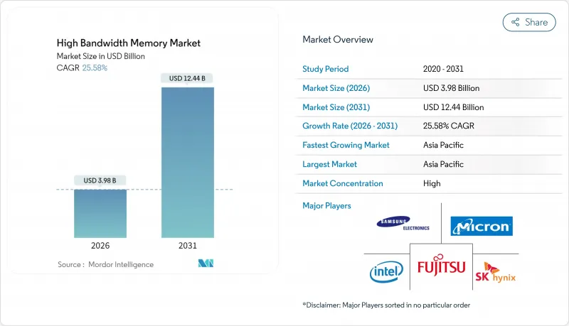
高频宽记忆体市场预计将从 2025 年的 31.7 亿美元成长到 2026 年的 39.8 亿美元,到 2031 年达到 124.4 亿美元,2026 年至 2031 年的复合年增长率为 25.58%。
2025年,对人工智慧优化伺服器的持续需求、DDR5记忆体的日益普及以及超大规模资料中心业者的大力投资,共同加速了半导体价值链的产能扩张。过去一年,供应商专注于提升TSV产量比率,而封装合作伙伴则投资建造新的CoWoS生产线以缓解基板短缺问题。汽车製造商加强了与记忆体供应商的合作,以确保为L3和L4级自动驾驶平台提供符合ISO 26262认证的HBM记忆体。亚太地区的製造业生态系统保持了其生产主导,韩国製造商承诺投入数十亿美元用于大规模生产下一代HBM4E记忆体。
全球高频宽记忆体市场趋势与洞察
AI伺服器和GPU连线速率的普及程度
大型语言模型的快速成长导致到 2024 年,每块 GPU 的 HBM 需求量将比传统 HPC 设备增加 7 倍。 NVIDIA 的 H100 配备 80GB HBM3 显存,传输速度为 3.35TB/s;而 H200 将于 2025 年初开始提供样品,配备 141GB HBM3E 显存,传输速度为 4.8TB/s。由于订单,供应商的大部分产能已预订至 2026 年,迫使资料中心营运商提前采购库存并共同投资建造封装生产线。
资料中心向DDR5和2.5D封装的迁移
超大规模资料中心业者已将工作负载从DDR4迁移到DDR5,从而实现了每瓦效能提升50%,同时也采用了2.5D整合技术,将AI加速器与堆迭式记忆体连接到硅中介层。然而,由于基板短缺导致GPU发布延迟至2024年,对单一包装平台的依赖增加了供应链风险。
TSV产量比率在12层以上堆迭结构中下降
在16层HBM堆迭结构中,由于热循环作用,TSV内部发生了铜迁移失效,导致产量比率降至70%以下。製造商正在研发热响应型TSV设计和新型介电材料以提高可靠性,但预计商业化还需要两年时间。
细分市场分析
到2025年,伺服器类别将占据高频宽记忆体市场67.80%的收入份额,这主要得益于超大规模营运商向整合8-12个HBM堆迭的AI伺服器转型。随着云端服务供应商推出基础模型服务,每个GPU的频宽需求超过3TB/s,市场需求加速成长。 2025年的能源效率目标有利于堆迭式DRAM,其每瓦效能优于独立解决方案,使资料中心营运商能够控制在电力预算范围内。企业更新换代週期已经启动,随着企业以支援HBM的加速器取代基于DDR4的节点,采购承诺已延续至2027年。
儘管目前汽车和交通运输领域规模较小,但预计到2031年,其复合年增长率将达到34.18%,成为成长最快的领域。晶片製造商正与一级供应商合作,将符合ASIL D要求的功能安全特性整合到晶片中。欧洲和北美的3级晶片生产项目将于2024年底开始小规模推广,届时车辆将利用传统上用于资料中心推理丛集的记忆体频宽。随着空中升级策略的日益成熟,汽车製造商正将车辆视为边缘伺服器,这将进一步推动HBM搭载率。
HBM3 在 AI 训练 GPU 的应用日益广泛,预计到 2025 年将贡献 45.70% 的收入。 HBM3E 样品于 2024 年第一季开始发放,首批量产产品的运作速度超过 9.2Gb/s。效能提升使每个堆迭的频宽达到 1.2TB/s,减少了达到目标频宽所需的堆迭数量,并降低了封装的热密度。
HBM3E预计40.90%的复合年增长率主要得益于美光36GB 12层高的产品,该产品将于2025年中期开始量产,目标应用是模型参数规模高达5200亿的加速器。展望未来,将于2025年4月发布的HBM4标准将使每个堆迭的通道数翻倍,并将总吞吐量提升至2TB/s,为多千万亿次浮点运算的AI处理器奠定基础。
高频宽记忆体 (HBM) 市场按应用(伺服器、网路、高效能运算、家用电子电器等)、技术(HBM2、HBM2E、HBM3、HBM3E、HBM4)、每个堆迭的记忆体容量(4GB、8GB、16GB、24GB、32GB+)、处理器电脑(GPU、CPU、AI 介面/A7等)和地区(北美、南美、欧洲、亚太、中东和非洲)进行细分。
区域分析
到2025年,亚太地区将占总营收的41.00%,其中韩国将扮演关键角色。 SK海力士和三星控制韩国超过80%的生产线。 2024年宣布的政府激励措施支持了计划于2027年投入运作的扩大型製造群。台湾台积电在尖端的CoWoS封装技术方面保持垄断地位,这使得记忆体供应依赖于本地基板供应,从而造成了区域集中度风险。
随着美光科技获得《晶片法案》61亿美元的资金筹措,用于在纽约州和爱达荷州建设先进的DRAM晶圆厂,北美市场份额有所增长,预计HBM试点生产将于2026年初开始。超大规模资料中心业者的资本支出继续推动当地需求,但大多数晶圆仍在亚洲製造,最终的模组组装则在美国进行。
欧洲市场受汽车需求驱动而进入。德国汽车製造商已完成L3级驾驶辅助系统的HBM认证,预计2024年底开始出货。欧盟的半导体策略仍以研发为中心,重点发展光子互连和神经形态技术,这对于未来扩大高频宽记忆体市场至关重要。虽然中东和非洲地区仍处于应用初期,但2025年国家主导的人工智慧资料中心计划显示该地区的需求正在成长。
其他福利:
- Excel格式的市场预测(ME)表
- 3个月的分析师支持
目录
第一章 引言
- 研究假设和市场定义
- 调查范围
第二章调查方法
第三章执行摘要
第四章 市场情势
- 市场概览
- 市场驱动因素
- AI伺服器的普及和搭载率
- 资料中心向DDR5和2.5D封装的迁移
- 边缘人工智慧推理在汽车ADAS的应用
- 超大规模资料中心业者对硅中介层堆迭的偏好
- 各地区(韩国、美国、日本)的记忆体生产补贴
- 光电赋能的HBM蓝图(HBM-P)
- 市场限制
- 12层堆迭结构中TSV产量比率损失
- CoWoS/SoIC先进封装能力有限
- 频宽大于 1TB/s 的设备出现热感节流现象
- 对人工智慧加速器的地缘政治出口管制
- 价值链分析
- 监管环境
- 技术展望
- 波特五力分析
- 供应商的议价能力
- 买方的议价能力
- 新进入者的威胁
- 替代品的威胁
- 竞争对手之间的竞争
- DRAM市场分析
- DRAM 收入及预测
- 各地区DRAM收入
- DDR5产品的当前价格
- DDR5产品製造商列表
- 宏观经济因素的影响
第五章 市场规模与成长预测
- 透过使用
- 伺服器
- 网路
- 高效能运算
- 家用电子电器
- 汽车和运输设备
- 透过技术
- HBM2
- HBM2E
- HBM3
- HBM3E
- HBM4
- 按记忆体容量(每个堆迭)
- 4 GB
- 8 GB
- 16 GB
- 24 GB
- 32 GB 或更多
- 透过处理器介面
- GPU
- CPU
- AI加速器/ASIC
- FPGA
- 其他的
- 按地区
- 北美洲
- 美国
- 加拿大
- 墨西哥
- 南美洲
- 巴西
- 南美洲其他地区
- 欧洲
- 德国
- 法国
- 英国
- 其他欧洲地区
- 亚太地区
- 中国
- 日本
- 印度
- 韩国
- 亚太其他地区
- 中东和非洲
- 中东
- 沙乌地阿拉伯
- 阿拉伯聯合大公国
- 土耳其
- 其他中东地区
- 非洲
- 南非
- 其他非洲地区
- 中东
- 北美洲
第六章 竞争情势
- 市场集中度
- 策略趋势
- 市占率分析
- 公司简介
- Samsung Electronics Co., Ltd.
- SK hynix Inc.
- Micron Technology, Inc.
- Intel Corporation
- Advanced Micro Devices, Inc.
- Nvidia Corporation
- Taiwan Semiconductor Manufacturing Company Limited
- ASE Technology Holding Co., Ltd.
- Amkor Technology, Inc.
- Powertech Technology Inc.
- United Microelectronics Corporation
- GlobalFoundries Inc.
- Applied Materials Inc.
- Marvell Technology, Inc.
- Rambus Inc.
- Cadence Design Systems, Inc.
- Synopsys, Inc.
- Siliconware Precision Industries Co., Ltd.
- JCET Group Co., Ltd.
- Chipbond Technology Corporation
- Cadence Design Systems Inc.
- Broadcom Inc.
- Celestial AI
- ASE-SPIL(Silicon Products)
- Graphcore Limited
第七章 市场机会与未来展望
The high bandwidth memory market is expected to grow from USD 3.17 billion in 2025 to USD 3.98 billion in 2026 and is forecast to reach USD 12.44 billion by 2031 at 25.58% CAGR over 2026-2031.
Sustained demand for AI-optimized servers, wider DDR5 adoption, and aggressive hyperscaler spending continued to accelerate capacity expansions across the semiconductor value chain in 2025. Over the past year, suppliers concentrated on TSV yield improvement, while packaging partners invested in new CoWoS lines to ease substrate shortages. Automakers deepened engagements with memory vendors to secure ISO 26262-qualified HBM for Level 3 and Level 4 autonomous platforms. Asia-Pacific's fabrication ecosystem retained production leadership after Korean manufacturers committed multibillion-dollar outlays aimed at next-generation HBM4E ramps.
Global High Bandwidth Memory Market Trends and Insights
AI-Server Proliferation and GPU Attach Rates
Rapid growth in large-scale language models drove a seven-fold rise in HBM per GPU requirements compared with traditional HPC devices during 2024. NVIDIA's H100 combined 80 GB of HBM3, delivering 3.35 TB/s, while the H200 was sampled in early 2025 with 141 GB of HBM3E at 4.8 TB/s. Order backlogs locked in the majority of supplier capacity through 2026, forcing data-center operators to pre-purchase inventory and co-invest in packaging lines.
Data-Center Shift to DDR5 and 2.5-D Packaging
Hyperscalers moved workloads from DDR4 to DDR5 to obtain 50% better performance per watt, simultaneously adopting 2.5-D integration that links AI accelerators to stacked memory on silicon interposers. Dependence on a single packaging platform heightened supply-chain risk when substrate shortages delayed GPU launches throughout 2024.
TSV Yield Losses Above 12-Layer Stacks
Yield fell below 70% on 16-high HBM stacks because thermal cycling induced copper-migration failures within TSVs. Manufacturers pursued thermal through-silicon via designs and novel dielectric materials to stabilize reliability, but commercialization remains two years away.
Other drivers and restraints analyzed in the detailed report include:
- Edge-AI Inference in Automotive ADAS
- Hyperscaler Preference for Silicon Interposer Stacks
- Limited CoWoS/SoIC Advanced-Packaging Capacity
For complete list of drivers and restraints, kindly check the Table Of Contents.
Segment Analysis
The server category led the high bandwidth memory market with a 67.80% revenue share in 2025, reflecting hyperscale operators' pivot to AI servers that each integrate eight to twelve HBM stacks. Demand accelerated after cloud providers launched foundation-model services that rely on per-GPU bandwidth above 3 TB/s. Energy efficiency targets in 2025 favored stacked DRAM because it delivered superior performance-per-watt over discrete solutions, enabling data-center operators to stay within power envelopes. An enterprise refresh cycle began as companies replaced DDR4-based nodes with HBM-enabled accelerators, extending purchasing commitments into 2027.
The automotive and transportation segment, while smaller today, recorded the fastest growth with a projected 34.18% CAGR through 2031. Chipmakers collaborated with Tier 1 suppliers to embed functional-safety features that meet ASIL D requirements. Level 3 production programs in Europe and North America entered limited rollout in late 2024, each vehicle using memory bandwidth previously reserved for data-center inference clusters. As over-the-air update strategies matured, vehicle manufacturers began treating cars as edge servers, further sustaining HBM attach rates.
HBM3 accounted for 45.70% revenue in 2025 after widespread adoption in AI training GPUs. Sampling of HBM3E started in Q1 2024, and first-wave production ran at pin speeds above 9.2 Gb/s. Performance gains reached 1.2 TB/s per stack, reducing the number of stacks needed for the target bandwidth and lowering package thermal density.
HBM3E's 40.90% forecast CAGR is underpinned by Micron's 36 GB, 12-high product that entered volume production in mid-2025, targeting accelerators with model sizes up to 520 billion parameters. Looking forward, the HBM4 standard published in April 2025 doubles channels per stack and raises aggregate throughput to 2 TB/s, setting the stage for multi-petaflop AI processors.
High Bandwidth Memory (HBM) Market is Segmented by Application (Servers, Networking, High-Performance Computing, Consumer Electronics, and More), Technology (HBM2, HBM2E, HBM3, HBM3E, and HBM4), Memory Capacity Per Stack (4 GB, 8 GB, 16 GB, 24 GB, and 32 GB and Above), Processor Interface (GPU, CPU, AI Accelerator/ASIC, FPGA, and More), and Geography (North America, South America, Europe, Asia-Pacific, and Middle East and Africa).
Geography Analysis
Asia-Pacific accounted for 41.00% of 2025 revenue, anchored by South Korea, where SK Hynix and Samsung controlled more than 80% of production lines. Government incentives announced in 2024 supported an expanded fabrication cluster scheduled to open in 2027. Taiwan's TSMC maintained a packaging monopoly for leading-edge CoWoS, tying memory availability to local substrate supply and creating a regional concentration risk.
North America's share grew as Micron secured USD 6.1 billion in CHIPS Act funding to build advanced DRAM fabs in New York and Idaho, with pilot HBM runs expected in early 2026. Hyperscaler capital expenditures continued to drive local demand, although most wafers were still processed in Asia before final module assembly in the United States.
Europe entered the market through automotive demand; German OEMs qualified HBM for Level 3 driver-assist systems shipping in late 2024. The EU's semiconductor strategy remained R&D-centric, favoring photonic interconnect and neuromorphic research that could unlock future high bandwidth memory market expansion. Middle East and Africa stayed in an early adoption phase, yet sovereign AI datacenter projects initiated in 2025 suggested a coming uptick in regional demand.
- Samsung Electronics Co., Ltd.
- SK hynix Inc.
- Micron Technology, Inc.
- Intel Corporation
- Advanced Micro Devices, Inc.
- Nvidia Corporation
- Taiwan Semiconductor Manufacturing Company Limited
- ASE Technology Holding Co., Ltd.
- Amkor Technology, Inc.
- Powertech Technology Inc.
- United Microelectronics Corporation
- GlobalFoundries Inc.
- Applied Materials Inc.
- Marvell Technology, Inc.
- Rambus Inc.
- Cadence Design Systems, Inc.
- Synopsys, Inc.
- Siliconware Precision Industries Co., Ltd.
- JCET Group Co., Ltd.
- Chipbond Technology Corporation
- Cadence Design Systems Inc.
- Broadcom Inc.
- Celestial AI
- ASE-SPIL (Silicon Products)
- Graphcore Limited
Additional Benefits:
- The market estimate (ME) sheet in Excel format
- 3 months of analyst support
TABLE OF CONTENTS
1 INTRODUCTION
- 1.1 Study Assumptions and Market Definition
- 1.2 Scope of the Study
2 RESEARCH METHODOLOGY
3 EXECUTIVE SUMMARY
4 MARKET LANDSCAPE
- 4.1 Market Overview
- 4.2 Market Drivers
- 4.2.1 AI-server proliferation and GPU attach rates
- 4.2.2 Data-center shift to DDR5 and 2.5-D packaging
- 4.2.3 Edge-AI inference in automotive ADAS
- 4.2.4 Hyperscaler preference for silicon interposer stacks
- 4.2.5 Localized memory production subsidies (KR, US, JP)
- 4.2.6 Photonics-ready HBM road-maps (HBM-P)
- 4.3 Market Restraints
- 4.3.1 TSV yield losses above 12-layer stacks
- 4.3.2 Limited CoWoS/SoIC advanced-packaging capacity
- 4.3.3 Thermal throttling in >1 TB/s bandwidth devices
- 4.3.4 Geo-political export controls on AI accelerators
- 4.4 Value Chain Analysis
- 4.5 Regulatory Landscape
- 4.6 Technological Outlook
- 4.7 Porter's Five Forces Analysis
- 4.7.1 Bargaining Power of Suppliers
- 4.7.2 Bargaining Power of Buyers
- 4.7.3 Threat of New Entrants
- 4.7.4 Threat of Substitutes
- 4.7.5 Intensity of Competitive Rivalry
- 4.8 DRAM Market Analysis
- 4.8.1 DRAM Revenue and Demand Forecast
- 4.8.2 DRAM Revenue by Geography
- 4.8.3 Current Pricing of DDR5 Products
- 4.8.4 List of DDR5 Product Manufacturers
- 4.9 Impact of Macroeconomic Factors
5 MARKET SIZE AND GROWTH FORECASTS (VALUE)
- 5.1 By Application
- 5.1.1 Servers
- 5.1.2 Networking
- 5.1.3 High-Performance Computing
- 5.1.4 Consumer Electronics
- 5.1.5 Automotive and Transportation
- 5.2 By Technology
- 5.2.1 HBM2
- 5.2.2 HBM2E
- 5.2.3 HBM3
- 5.2.4 HBM3E
- 5.2.5 HBM4
- 5.3 By Memory Capacity per Stack
- 5.3.1 4 GB
- 5.3.2 8 GB
- 5.3.3 16 GB
- 5.3.4 24 GB
- 5.3.5 32 GB and Above
- 5.4 By Processor Interface
- 5.4.1 GPU
- 5.4.2 CPU
- 5.4.3 AI Accelerator / ASIC
- 5.4.4 FPGA
- 5.4.5 Others
- 5.5 By Geography
- 5.5.1 North America
- 5.5.1.1 United States
- 5.5.1.2 Canada
- 5.5.1.3 Mexico
- 5.5.2 South America
- 5.5.2.1 Brazil
- 5.5.2.2 Rest of South America
- 5.5.3 Europe
- 5.5.3.1 Germany
- 5.5.3.2 France
- 5.5.3.3 United Kingdom
- 5.5.3.4 Rest of Europe
- 5.5.4 Asia-Pacific
- 5.5.4.1 China
- 5.5.4.2 Japan
- 5.5.4.3 India
- 5.5.4.4 South Korea
- 5.5.4.5 Rest of Asia-Pacific
- 5.5.5 Middle East and Africa
- 5.5.5.1 Middle East
- 5.5.5.1.1 Saudi Arabia
- 5.5.5.1.2 United Arab Emirates
- 5.5.5.1.3 Turkey
- 5.5.5.1.4 Rest of Middle East
- 5.5.5.2 Africa
- 5.5.5.2.1 South Africa
- 5.5.5.2.2 Rest of Africa
- 5.5.5.1 Middle East
- 5.5.1 North America
6 COMPETITIVE LANDSCAPE
- 6.1 Market Concentration
- 6.2 Strategic Moves
- 6.3 Market Share Analysis
- 6.4 Company Profiles (includes Global-level Overview, Market-level Overview, Core Segments, Financials, Strategic Information, Market Rank/Share, Products and Services, Recent Developments)
- 6.4.1 Samsung Electronics Co., Ltd.
- 6.4.2 SK hynix Inc.
- 6.4.3 Micron Technology, Inc.
- 6.4.4 Intel Corporation
- 6.4.5 Advanced Micro Devices, Inc.
- 6.4.6 Nvidia Corporation
- 6.4.7 Taiwan Semiconductor Manufacturing Company Limited
- 6.4.8 ASE Technology Holding Co., Ltd.
- 6.4.9 Amkor Technology, Inc.
- 6.4.10 Powertech Technology Inc.
- 6.4.11 United Microelectronics Corporation
- 6.4.12 GlobalFoundries Inc.
- 6.4.13 Applied Materials Inc.
- 6.4.14 Marvell Technology, Inc.
- 6.4.15 Rambus Inc.
- 6.4.16 Cadence Design Systems, Inc.
- 6.4.17 Synopsys, Inc.
- 6.4.18 Siliconware Precision Industries Co., Ltd.
- 6.4.19 JCET Group Co., Ltd.
- 6.4.20 Chipbond Technology Corporation
- 6.4.21 Cadence Design Systems Inc.
- 6.4.22 Broadcom Inc.
- 6.4.23 Celestial AI
- 6.4.24 ASE-SPIL (Silicon Products)
- 6.4.25 Graphcore Limited
7 MARKET OPPORTUNITIES AND FUTURE OUTLOOK
- 7.1 White-space and Unmet-need Assessment
 2026年全球高频宽记忆体(HBM)市场报告2026年混合储存立方体(HMC)全球市场报告
 HBM晶片市场按类型、储存容量、介面类型、应用和最终用户产业划分-2026-2032年全球预测
 混合记忆体立方体市场-全球产业规模、份额、趋势、机会和预测,按产品类型、应用(高效能运算、网路、资料中心和图形)、地区和竞争格局划分,2021-2031年预测
 高频宽记忆体市场预测至2032年:按记忆体类型、介面类型、部署方式、应用领域、最终用户和地区分類的全球分析
 混合储存立方体的全球市场混合记忆体立方体 (HMC) 市场预测(至 2032 年):按产品类型、记忆体类型、处理器相容性、记忆体配置、应用、最终用户和地区进行的全球分析
 2025 年至 2033 年混合记忆体立方体市场规模、份额、趋势及预测(按产品、应用、最终用途产业和地区)
 高频宽记忆体市场机会、成长动力、产业趋势分析及 2025 - 2034 年预测
 HMC(混合记忆体立方体):市场占有率分析、产业趋势与统计、成长预测(2025-2030)