


 |
市场调查报告书
商品编码
1937414
共封装光学元件(CPO):市场占有率分析、产业趋势与统计、成长预测(2026-2031)Co-packaged Optics - Market Share Analysis, Industry Trends & Statistics, Growth Forecasts (2026 - 2031) |
||||||
※ 本网页内容可能与最新版本有所差异。详细情况请与我们联繫。
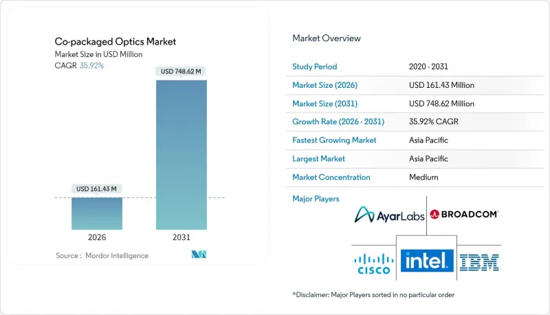
预计到 2025 年,共封装光学元件 (CPO) 市值将达到 1.2 亿美元,从 2026 年的 1.6 亿美元成长到 2031 年的 7.5 亿美元。
预计在预测期(2026-2031 年)内,复合年增长率将达到 35.92%。
硅光电整合技术最初主要处于实验阶段,如今受益于半导体製造的大规模生产和先进的封装技术,使超大规模营运商能够在降低电力消耗的同时,实现与 51.2 Tbps交换器硅晶相当的频宽密度。其成长动力源自于三大互补趋势:(1) 人工智慧训练丛集需要比传统云端架构更高的东西向频宽;(2) 北美和欧盟的能源效率法规优先考虑降低每Gigabit瓦功耗的解决方案;(3) 代工厂的普及(尤其是台积电的硅光电封装专案)降低了每条光通道的成本并产量比率了良率。由于光元件供应商、半导体製造商和新兴的硅光电专家都在竞相解决供应阻碍因素的异质整合难题,市场竞争仍然激烈。随着开放运算社群不断完善介面规范,共封装光元件市场可望从早期采用者阶段过渡到主流资料中心基础架构阶段。
全球共封装光学元件 (CPO) 市场趋势与洞察
51.2T交换器硅晶的量产需要1.6T CPO
博通的Bailly平台证明,在其Tomahawk 5交换器中整合八个6.4Tbps光引擎,与可插拔收发器相比,功耗降低了70%。由于传统电缆无法维持51.2Tbps ASIC所需的讯号完整性,超大规模营运商被迫重新评估其网路拓扑结构。 800G可插拔设备的机架级散热设计预算已接近实际极限,这加剧了经济差距,并促使采购部门将共封装光模组(CPO)视为必备技术,而非实验性计划。随着第三代200Gbit/s通道的CPO进入量产阶段,共封装光模组市场如今拥有了清晰的技术蓝图,与2026-2028年的交换器硅晶更新周期相契合。这使得设备OEM厂商能够加快设计采用速度,并确保中期需求的可预测性。
超大规模资料中心的节能要求
随着各大云端服务供应商宣布净零排放承诺,每Gigabit的电力消耗量指标日益受到关注。日月光(ASE)展示的低于5pJ/bit的光引擎证实,将光模组整合到交换器封装内可以降低DSP功耗并消除铜互连损耗。从欧盟碳定价机製到城市层级暂停新建资料中心,监管压力使得降低功耗成为基板挑战。业者提出与节能相关的三年投资回收期目标,同时推广采用共封装光学模组,以此在不超出站点电力预算的情况下提高机架密度。这种政策环境正在将技术优势转化为投资动力,并透过长期采购协议推动需求成长。
製造复杂性和异质整合带来回报
共封装光学元件 (CPO) 将硅光电、III-V族雷射和先进基板整合到毫米级机壳中。在键结高功率晶粒的同时,以数十奈米的精度对准光波导会在多个製程步骤中引入损耗。 NVIDIA 先进的 CoWoS 生产线在 Blackwell 量产爬坡阶段的产量比率下降凸显了此製程视窗的脆弱性。材料不匹配导致的热应力需要特殊的界面层和主动冷却,从而增加了元件数量和检测步骤。在技术成熟之前,批量供应将受到限制,这将延长二级 OEM 厂商的前置作业时间,并抑制共封装光学元件市场近期的出货量预测。
细分市场分析
到2025年,3.2 Tbps光模组将占共封装光模组市场收入的37.92%,这反映了Tomahawk 4级交换器的装置量。然而,随着人工智慧丛集对更高速率光纤网路的需求不断增长,6.4 Tbps及更高速率的设备到2031年将以58.64%的复合年增长率成长。将单一6.4 Tbps引擎与51.2 Tbps ASIC晶片集成,可实现8条200 Gbit/s的光通道。这不仅将交换器到模组的功耗预算减半,还省去了重定时器级。厂商已製定了6.4 Tbps及更高速率蓝图,以配合2026年及以后的伺服器更新周期。
展望未来,晶圆代工厂的蓝图预测,12.8 Tbps 的引擎将在单一封装内堆迭多个光核心,其中最高频宽预计将超过所有其他资料速率等级。虽然低于 1.6 Tbps 的共封装光模组 (CPO) 仍然适用于成本优先于密度的边缘设备,但超大规模竞标檔案现在已将 200G/通道的讯号路径指定为标准。随着这一转变的推进,预计到 2029 年,用于 6.4 Tbps 及更高速率设备的共封装光模组的市场价值将超过所有低速率光模组市场价值的总和。
到2025年,光学引擎将占总收入的41.12%,而随着厂商掌握片上发光技术,雷射光源的复合年增长率将达到43.71%。采用中国产200mm硅晶圆製造的整合式磷化铟雷射阵列无需外部泵浦雷射器,并降低了封装高度,从而降低了材料成本并提高了可靠性。
由于控制器功能整合在封装内,电子积体电路的需求保持稳定,但其附加价值来源正转向雷射技术创新。整合光源无需光纤尾纤,使系统设计人员能够实现更薄的机架顶部交换机,从而释放前面板空间。因此,在超超大规模资料中心业者和雷射代工厂之间签订的多年供应协议的支持下,用于雷射元件的共封装光学元件的市场规模正从利基市场转向核心市场。
共封装光学元件 (CPO) 市场按资料速率(<1.6T、1.6T、3.2T 以上)、元件(光引擎、电子 IC、雷射源、连接器、封装等)、整合方法(板载光学元件、共封装光学元件)、最终用途(超大规模资料中心业者、资料中心、整合方法(板载光学元件、共封装光学元件)、最终用途(美国通讯业者和欧洲地区运营商、北美地区、其他地区)。
区域分析
亚太地区预计到2025年将占全球营收的32.78%,年复合成长率达41.99%,主要得益于政府补贴和垂直整合的供应链。中国82亿元人民币(约1300亿日元)的补贴推动了8英寸硅光子光电的生产和雷射集成,从而降低了元器件成本。日本经济产业省已拨款3.05亿美元给NTT、英特尔和SK海力士,用于共同开发光晶片,从而加强日本国内的设计生态系统。韩国正透过调整其高频宽蓝图,使其与光介面技术相契合,从而对这项合作做出补充。
北美透过超大规模营运商满足了大部分终端用户需求。博通、英特尔和英伟达是该地区技术基础的支柱,而台积电位于亚利桑那州的晶圆厂则引入了本土封装能力,从而缩短了美国云端客户的前置作业时间。因此,共封装光学元件市场受益于晶片设计与内部消费相结合的闭合迴路,即使生产日益分散于全球各地,也巩固了该地区的市场份额。
互通性和永续性是欧洲的优先事项。总部位于欧盟的开放运算专案(OCP)负责开发介面设计并制定全球部署实务。碳定价立法进一步推动了部署,营运商透过将可插拔光学模组转向共封装装置,实现了30%至50%的节能。併购活动,例如诺基亚以23亿美元收购Infinera,显示该地区有意确保自身光纤通讯智慧财产权并提升价值链地位。
其他福利:
- Excel格式的市场预测(ME)表
- 3个月的分析师支持
目录
第一章 引言
- 研究假设和市场定义
- 调查范围
第二章调查方法
第三章执行摘要
第四章 市场情势
- 市场概览
- 市场驱动因素
- 51.2 T交换器硅晶大规模生产(需 1.6 T CPO)
- 超大规模资料中心能源效率强制性要求
- AI/ML丛集频宽需求激增
- 800G/1.6T 可插拔过渡件达到热极限
- 透过代工厂参与实现大规模生产的经济效益(例如,台积电 COUPE 专案)
- 透过开放式运算主导的首席产品长 (CPO) 协作减少供应商锁定
- 市场限制
- 製造复杂性与异质整合产量比率
- 互通性和标准的不成熟
- 光学模组所有权转移至交换器ASIC供应商
- 光子封装技能差距
- 价值链分析
- 监管环境
- 技术展望
- 宏观经济因素的影响
- 对延迟敏感型流量的影响
- 波特五力分析
- 新进入者的威胁
- 买方的议价能力
- 供应商的议价能力
- 替代品的威胁
- 竞争对手之间的竞争
- 投资与资金筹措分析
第五章 市场规模与成长预测
- 按数据速率
- 小于1.6吨
- 1.6 T
- 3.2 T
- 6.4吨或以上
- 按组件
- 轻型引擎
- 积体电路
- 雷射光源
- 连接器和包装
- 其他的
- 透过整合方法
- 机载光学设备
- 共封装光学元件
- 按最终用途
- 超大规模云端资料中心
- 企业资料中心
- 通讯业者中心局
- 高效能运算和人工智慧/机器学习丛集
- 其他的
- 按地区
- 北美洲
- 我们
- 加拿大
- 南美洲
- 巴西
- 其他南美洲
- 欧洲
- 德国
- 英国
- 法国
- 荷兰
- 其他欧洲地区
- 亚太地区
- 中国
- 日本
- 韩国
- 印度
- 亚太其他地区
- 中东和非洲
- 中东
- 以色列
- 土耳其
- GCC
- 其他中东地区
- 非洲
- 南非
- 其他非洲地区
- 中东
- 北美洲
第六章 竞争情势
- 市场集中度
- 策略趋势
- 市占率分析
- 公司简介
- Ayar Labs Inc.
- Broadcom Inc.
- Cisco Systems Inc.
- IBM Corporation
- Intel Corporation
- Ranovus Inc.
- TE Connectivity Ltd.
- Furukawa Electric Co., Ltd.
- Hisense Broadband Multimedia Technology Co., Ltd.
- POET Technologies Inc.
- Kyocera Corporation
- HiSilicon(Huawei Technologies Co., Ltd.)
- SENKO Advanced Components, Inc.
- Sumitomo Electric Industries, Ltd.
- Coherent Corp.
- Taiwan Semiconductor Manufacturing Company Limited(TSMC)
- Lumentum Holdings Inc.
- NVIDIA Corporation
- Marvell Technology, Inc.
- Ciena Corporation
- Nokia Corporation
- InnoLight Technology(Suzhou)Ltd.
- Acacia Communications Inc.
- Hon Hai Precision Industry Co., Ltd.(Foxconn)
- Jabil Inc.
第七章 市场机会与未来展望
The co-packaged optics market was valued at USD 0.12 billion in 2025 and estimated to grow from USD 0.16 billion in 2026 to reach USD 0.75 billion by 2031, at a CAGR of 35.92% during the forecast period (2026-2031).
Silicon photonics integration, once largely experimental, now benefits from high-volume semiconductor manufacturing and advanced packaging, enabling hyperscale operators to pursue bandwidth densities that match 51.2 Tbps switch silicon while lowering power budgets. Growth momentum stems from three reinforcing trends: (1) AI training clusters require far denser east-west bandwidth than classic cloud architectures, (2) energy-efficiency mandates in North America and the EU prioritize solutions that trim watt-per-gigabit metrics, and (3) foundry participation-most visibly TSMC's silicon-photonics packaging programs-reduces cost per optical lane and improves yield. Competitive intensity remains high as optical component vendors, semiconductor houses, and new silicon-photonics specialists race to solve heterogeneous-integration challenges that still constrain supply. As open compute communities refine interface specifications, the co-packaged optics market is positioned to shift from early adopter status to mainstream data-center infrastructure.
Global Co-packaged Optics Market Trends and Insights
Ramp-up of 51.2T switch silicon requiring 1.6T CPO
Broadcom's Bailly platform showed how embedding eight 6.4 Tbps optical engines beside a Tomahawk 5 switch delivered 70% lower power draw than pluggable transceivers. Hyperscale operators consequently reassessed network topologies because legacy electrical traces could not sustain the signal integrity demanded by 51.2 Tbps ASICs. The economic gap widened when rack-level thermal budgets for 800G pluggables hit practical ceilings, prompting procurement teams to treat co-packaged optics as a necessity rather than a lab project. As the third-generation CPO with 200 Gbit/s lanes enters production, the co-packaged optics market gains a clear technical roadmap that aligns with 2026-2028 switch-silicon refresh cycles. Equipment OEMs, therefore, accelerate design wins, locking in demand visibility over the medium term.
Hyperscale data-center energy-efficiency mandates
Net-zero pledges published by major cloud providers intensified scrutiny on watts-per-gigabit metrics. ASE's demonstration of <5 pJ/bit optical engines confirmed that integrating optics inside the switch package cuts DSP power and eliminates copper trace losses. Regulatory pressure-from carbon-pricing schemes in the EU to city-level moratoriums on new data-center builds-made the power reduction a board-level issue. Operators outlined three-year payback targets tied to energy savings and, in parallel, positioned co-packaged optics as a lever to unlock higher rack densities without breaching site power envelopes. The policy environment, therefore, transforms a technical benefit into an investment imperative, boosting demand through long-term purchase agreements.
Manufacturing complexity and heterogeneous integration yield
Co-packaged optics combines silicon photonics, III-V lasers, and advanced substrates inside a millimeter-scale envelope. Aligning optical waveguides to within tens of nanometers while also attaching high-power switch dice drives yields loss across multiple process steps. Recent yield slippages in advanced CoWoS lines, highlighted during NVIDIA's Blackwell ramp, underscore the fragile process window. Material-mismatch thermal stress necessitates exotic interface layers and active cooling, increasing part counts and inspection steps. Until learning curves mature, volume availability remains constrained, elongating lead times for tier-two OEMs and tempering near-term shipment forecasts for the co-packaged optics market.
Other drivers and restraints analyzed in the detailed report include:
- Surge in AI/ML cluster bandwidth demand
- Foundry participation enabling volume economics
- Interoperability and standards immaturity
For complete list of drivers and restraints, kindly check the Table Of Contents.
Segment Analysis
The 3.2 Tbps segment accounted for 37.92% of the co-packaged optics market revenue in 2025, reflecting the installed base of Tomahawk 4 class switches. However, >=6.4 Tbps devices are posting a 58.64% CAGR through 2031 as AI clusters press for higher radix fabrics. A single 6.4 Tbps engine co-located with a 51.2 Tbps ASIC yields eight optical lanes at 200 Gbit/s each, which halves the switch-to-module power budget and eliminates retimer stages. Vendors thus lock the >=6.4 Tbps roadmap into server refresh cycles beginning in 2026.
Looking forward, the foundry roadmaps project 12.8 Tbps engines that stack multiple optical cores within one package, positioning the top-end band to outgrow all other data-rate tiers. While sub-1.6 Tbps CPO remains viable for edge appliances where cost outranks density, hyperscale bidding documents now stipulate 200G/lane signal paths as a baseline. As this migration unfolds, the co-packaged optics market size for >=6.4 Tbps devices is set to outstrip the combined value of lower speed classes by 2029.
Optical engines represented 41.12% of 2025 revenue, yet laser sources are expanding at a 43.71% CAGR as vendors master on-chip light generation. China's integrated indium-phosphide laser arrays, produced on 200 mm silicon wafers, removed the need for external pump lasers and reduced package height, trimming material cost, and improved reliability.
Electronics ICs maintain steady demand as controller functions migrate on-package, but the incremental value pool is shifting toward laser innovation. With integrated sources eliminating fiber pigtails, system architects design slimmer top-of-rack switches and free front-panel real estate. The co-packaged optics market size for laser devices is therefore moving from niche to core, supported by multi-year supply agreements between hyperscalers and laser foundries.
Co-Packaged Optics Market is Segmented by Data Rate (< 1. 6T, 1. 6T, 3. 2T, and Above), Component (Optical Engine, Electrical IC, Laser Source, Connector and Packaging, and More), Integration Approach (On-Board Optics, and Co-Packaged Optics), End-Use Application (Hyperscale Cloud Data Centers, Enterprise Data Centers, and More), and Geography (North America, South America, Europe, Asia-Pacific, and Middle East and Africa).
Geography Analysis
Asia-Pacific commanded 32.78% of 2025 revenue and is advancing at a 41.99% CAGR, powered by government subsidies and vertically integrated supply. China's CNY 8.2 billion subsidy enabled eight-inch silicon-photonics wafer production and laser integration that compresses the bill-of-materials cost. Japan's Ministry of Economy, Trade and Industry funded USD 305 million for NTT, Intel, and SK Hynix to co-develop optical chips, strengthening local design ecosystems. South Korea complements the loop by aligning high-bandwidth memory roadmaps with optical interfaces.
North America supplies the bulk of end-user demand through hyperscale operators. Broadcom, Intel, and NVIDIA anchor the regional technology stack, while TSMC's Arizona fabs introduce domestic packaging capacity that shortens lead times for US cloud customers. The co-packaged optics market, therefore, benefits from a closed loop that links chip design to captive consumption, reinforcing the region's share even as production diversifies globally.
Europe prioritizes interoperability and sustainability. Open Compute Project chapters headquartered in the EU draft interface blueprints, shaping global deployment practices. Carbon-pricing legislation further propels adoption; operators document 30-50% power savings when shifting from pluggable optics to co-packaged lanes. M&A activity, typified by Nokia's USD 2.3 billion acquisition of Infinera, signals the region's intent to secure proprietary optical IP and climb the value chain.
- Ayar Labs Inc.
- Broadcom Inc.
- Cisco Systems Inc.
- IBM Corporation
- Intel Corporation
- Ranovus Inc.
- TE Connectivity Ltd.
- Furukawa Electric Co., Ltd.
- Hisense Broadband Multimedia Technology Co., Ltd.
- POET Technologies Inc.
- Kyocera Corporation
- HiSilicon (Huawei Technologies Co., Ltd.)
- SENKO Advanced Components, Inc.
- Sumitomo Electric Industries, Ltd.
- Coherent Corp.
- Taiwan Semiconductor Manufacturing Company Limited (TSMC)
- Lumentum Holdings Inc.
- NVIDIA Corporation
- Marvell Technology, Inc.
- Ciena Corporation
- Nokia Corporation
- InnoLight Technology (Suzhou) Ltd.
- Acacia Communications Inc.
- Hon Hai Precision Industry Co., Ltd. (Foxconn)
- Jabil Inc.
Additional Benefits:
- The market estimate (ME) sheet in Excel format
- 3 months of analyst support
TABLE OF CONTENTS
1 INTRODUCTION
- 1.1 Study Assumptions and Market Definition
- 1.2 Scope of the Study
2 RESEARCH METHODOLOGY
3 EXECUTIVE SUMMARY
4 MARKET LANDSCAPE
- 4.1 Market Overview
- 4.2 Market Drivers
- 4.2.1 Ramp-up of 51.2 T switch silicon requiring 1.6 T CPO
- 4.2.2 Hyperscale data-center energy-efficiency mandates
- 4.2.3 Surge in AI/ML cluster bandwidth demand
- 4.2.4 Transition to 800 G/1.6 T pluggables hitting thermal limits
- 4.2.5 Foundry participation (e.g., TSMC COUPE) enabling volume economics
- 4.2.6 Open Compute-driven CPO collaboration reducing vendor lock-in
- 4.3 Market Restraints
- 4.3.1 Manufacturing complexity and heterogeneous-integration yield
- 4.3.2 Interoperability and standards immaturity
- 4.3.3 Shift of optical-module ownership to switch-ASIC vendors
- 4.3.4 Photonic-packaging workforce skills gap
- 4.4 Value Chain Analysis
- 4.5 Regulatory Landscape
- 4.6 Technological Outlook
- 4.7 Impact of Macroeconomic Factors
- 4.8 Latency-Sensitive Traffic Impact
- 4.9 Porter's Five Forces Analysis
- 4.9.1 Threat of New Entrants
- 4.9.2 Bargaining Power of Buyers
- 4.9.3 Bargaining Power of Suppliers
- 4.9.4 Threat of Substitutes
- 4.9.5 Intensity of Competitive Rivalry
- 4.10 Investment and Funding Analysis
5 MARKET SIZE AND GROWTH FORECASTS (VALUE)
- 5.1 By Data Rate
- 5.1.1 < 1.6 T
- 5.1.2 1.6 T
- 5.1.3 3.2 T
- 5.1.4 6.4 T and Above
- 5.2 By Component
- 5.2.1 Optical Engine
- 5.2.2 Electrical IC
- 5.2.3 Laser Source
- 5.2.4 Connector and Packaging
- 5.2.5 Others
- 5.3 By Integration Approach
- 5.3.1 On-board Optics
- 5.3.2 Co-packaged Optics
- 5.4 By End-use Application
- 5.4.1 Hyperscale Cloud Data Centers
- 5.4.2 Enterprise Data Centers
- 5.4.3 Telco Central Offices
- 5.4.4 HPC and AI/ML Clusters
- 5.4.5 Others
- 5.5 By Geography
- 5.5.1 North America
- 5.5.1.1 United States
- 5.5.1.2 Canada
- 5.5.2 South America
- 5.5.2.1 Brazil
- 5.5.2.2 Rest of South America
- 5.5.3 Europe
- 5.5.3.1 Germany
- 5.5.3.2 United Kingdom
- 5.5.3.3 France
- 5.5.3.4 Netherlands
- 5.5.3.5 Rest of Europe
- 5.5.4 Asia-Pacific
- 5.5.4.1 China
- 5.5.4.2 Japan
- 5.5.4.3 South Korea
- 5.5.4.4 India
- 5.5.4.5 Rest of Asia-Pacific
- 5.5.5 Middle East and Africa
- 5.5.5.1 Middle East
- 5.5.5.1.1 Israel
- 5.5.5.1.2 Turkey
- 5.5.5.1.3 GCC
- 5.5.5.1.4 Rest of Middle East
- 5.5.5.2 Africa
- 5.5.5.2.1 South Africa
- 5.5.5.2.2 Rest of Africa
- 5.5.5.1 Middle East
- 5.5.1 North America
6 COMPETITIVE LANDSCAPE
- 6.1 Market Concentration
- 6.2 Strategic Moves
- 6.3 Market Share Analysis
- 6.4 Company Profiles (includes Global level Overview, Market level overview, Core Segments, Financials, Strategic Information, Market Rank/Share, Products and Services, Recent Developments)
- 6.4.1 Ayar Labs Inc.
- 6.4.2 Broadcom Inc.
- 6.4.3 Cisco Systems Inc.
- 6.4.4 IBM Corporation
- 6.4.5 Intel Corporation
- 6.4.6 Ranovus Inc.
- 6.4.7 TE Connectivity Ltd.
- 6.4.8 Furukawa Electric Co., Ltd.
- 6.4.9 Hisense Broadband Multimedia Technology Co., Ltd.
- 6.4.10 POET Technologies Inc.
- 6.4.11 Kyocera Corporation
- 6.4.12 HiSilicon (Huawei Technologies Co., Ltd.)
- 6.4.13 SENKO Advanced Components, Inc.
- 6.4.14 Sumitomo Electric Industries, Ltd.
- 6.4.15 Coherent Corp.
- 6.4.16 Taiwan Semiconductor Manufacturing Company Limited (TSMC)
- 6.4.17 Lumentum Holdings Inc.
- 6.4.18 NVIDIA Corporation
- 6.4.19 Marvell Technology, Inc.
- 6.4.20 Ciena Corporation
- 6.4.21 Nokia Corporation
- 6.4.22 InnoLight Technology (Suzhou) Ltd.
- 6.4.23 Acacia Communications Inc.
- 6.4.24 Hon Hai Precision Industry Co., Ltd. (Foxconn)
- 6.4.25 Jabil Inc.
7 MARKET OPPORTUNITIES AND FUTURE OUTLOOK
- 7.1 White-space and Unmet-need Assessment
 共封装光学元件市场:依组件、材料、资料传输速率、外形规格及应用划分-2026-2032年全球市场预测
 全球共封装光元件(CPO)模组市场洞察及预测(至2033年)
 共封装光元件 (CPO) 在人工智慧资料中心的应用:十年市场与技术预测
 共封装光元件市场规模、份额及成长分析(按组件、资料速率、应用和地区划分)-2026-2033年产业预测
 全球共封装光元件 (CPO) 市场 (2026-2036)
 共封装光模组(CPO)-全球市场占有率和排名、总收入和需求预测(2025-2031年)硅光电和共封装光学元件测试与测量设备市场(按类型、测试阶段、最终用户和分销管道)—2025-2030 年全球预测
 全球共封装光学市场
 共封装光学元件 (CPO) 市场报告:2031 年趋势、预测与竞争分析