


 |
市场调查报告书
商品编码
1939018
先进封装:市场占有率分析、产业趋势与统计、成长预测(2026-2031)Advanced Packaging - Market Share Analysis, Industry Trends & Statistics, Growth Forecasts (2026 - 2031) |
||||||
※ 本网页内容可能与最新版本有所差异。详细情况请与我们联繫。
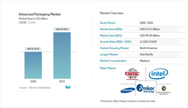
预计先进封装市场将从 2025 年的 516.2 亿美元成长到 2026 年的 575.7 亿美元,到 2031 年将达到 993.9 亿美元,2026 年至 2031 年的复合年增长率为 11.53%。
由于异质整合对于人工智慧 (AI) 处理器至关重要,而传统封装的散热和互连能力又无法满足需求,因此市场需求超出了最初的预期。为因应这项需求,整合装置製造商 (IDM) 和外包半导体组装测试 (OSAT) 服务商加快了资本投资,各国政府也推出了大规模激励措施,以促进组装能的本土化。先进封装市场也受惠于玻璃芯基板的研发、面板级加工的试点部署以及超大规模资料中心对光共封装技术的快速应用。然而,由于 BT 树脂基板短缺和工程人才匮乏,产能扩张无法及时进行,导致供应仍然紧张。随着晶圆代工厂将封装业务内部化以确保对 AI 供应链的端到端控制,竞争日益激烈,传统 OSAT 服务商的利润空间受到挤压,并促使其进行策略性专业化转型。
全球先进封装市场趋势与洞察
人工智慧和高效能运算对异质整合的需求日益增长
人工智慧工作负载对运算密度和记忆体频宽的要求远超传统封装技术。台积电的CoWoS平台将晶片组和高频宽记忆体整合于单一结构中,正迅速被主流人工智慧加速器厂商所采用。三星的SAINT技术采用混合键结技术实现下一代HBM4堆迭,也达到了类似的目标,凸显了自主研发先进封装技术的战略价值。热感界面材料、专用基板和主动中介层的引入,使得封装成本占半导体製造材料总成本的15%至20%(相较之下,主流CPU的封装成本仅占5%至8%)。因此,先进封装产能与尖端晶圆厂同等重要,共同决定人工智慧系统的上市时间。由此可见,先进封装市场的发展与前端製程的转型同步进行,而非落后于其后。
消费性电子设备的微型化推动了WLP技术的普及。
智慧型手机、穿戴式装置和耳机等装置对超薄设计和功能密度提出了更高的要求。扇出型晶圆级封装 (FOWLP) 能够将多个晶粒整合到厚度小于 0.5 毫米的超薄封装中,从而在不牺牲散热性能的前提下支援旗舰级移动处理器。从扇入型晶圆级封装 (WLP) 过渡到 FOWLP 可省去底部填充、焊线和层压基板等工序,从而降低高达 25% 的系统总成本。小型化趋势也延伸到了植入式医疗电子产品领域,尺寸在这个领域至关重要。无引线封装製造商利用 WLP 技术将元件尺寸缩小了 93%,同时满足了严格的可靠性要求。因此,消费和医疗领域的需求构成了可持续的基础,保护了先进封装市场免受个人电脑终端市场週期性波动的影响。
高资本密集度限制了市场进入。
2.5D 和 3D 製程的设备成本将达到每腔室 1,000 万至 1,500 万美元,远高于传统生产线通常的 300 万美元。台积电已为 2025 年的资本支出预算了 420 亿美元,其中很大一部分将用于先进封装的扩张。这使得规模较小的 OSAT(外包半导体组装和测试)厂商难以在产品生命週期快速缩短的情况下摊销投资,迫使它们专注于细分领域并进行防御性併购。预计如此高的门槛将扩大顶级公司与区域追随者之间的技术差距,从而在 2024 年至 2026 年期间限制先进封装市场的新增资本支出。
细分市场分析
受消费性电子和工业应用的大批量需求驱动,覆晶封装将在2025年继续保持领先地位,占据48.30%的市场份额。然而,2.5D/3D封装将实现最快成长,预计复合年增长率将达到13.05%,因为人工智慧加速器需要逻辑和记忆体接近性,而这超出了覆晶的限制。预计到2031年,2.5D/3D解决方案的先进封装市场规模将达到389亿美元,占平台总收入的39.15%。
三星的SAINT平台实现了10μm以下的混合键合,与焊线相比,讯号延迟降低了30%,热裕度提高了40%。台积电的CoWoS在2025年新增了三条生产线,消除了12个月的订单。嵌入式晶粒和扇出型WLP封装发展成为互补的选择:嵌入式封装满足了空间受限的汽车产业的需求,而扇出型WLP封装则应用于5G基地台和毫米波雷达设计。这些趋势共同推动了2.5D/3D封装在下一代装置发展蓝图中占据核心地位,巩固了其作为先进封装市场关键价值驱动因素的地位。
2025年,家用电子电器将占总出货量的39.20%,但其成长率将趋于个位数。相较之下,汽车和电动车的需求预计将以12.32%的复合年增长率成长,到2031年,其在先进封装市场的份额将提升至18.6%。预计到预测期结束时,汽车电子先进封装的市场规模将超过185亿美元。
目前,电动车牵引逆变器、车载充电器和网域控制器均采用车规级扇出型双面冷却功率模组和射出成型的系统级封装(SiP) 组件。资料中心基础设施是另一个高成长领域。人工智慧伺服器采用先进封装技术,可实现接近 1000 W/cm² 的功率密度,这需要开发创新的热感盖和底部填充材料。同时,医疗产业需要生物相容性涂层和密封外壳,这导致平均售价更高,且替换需求稳定。这些细分领域的趋势共同促成了收入来源的多元化,并降低了先进封装市场对智慧型手机更新周期的依赖。
先进封装市场按封装平台(覆晶、嵌入式晶粒、扇入式晶圆级封装等)、终端用户产业(家用电子电器、汽车/电动车、资料中心/高效能运算等)、装置架构(2D IC、2.5D 中介层、3D IC)、南美洲互通技术(焊料凸块、铜柱、混合键结)及欧洲地区(北美、非洲、亚焊球、铜柱、混合键结)及欧洲地区(北美、非洲、亚焊球、铜柱、混合键结)及欧洲地区(北美、非洲、欧洲地区)。
区域分析
到2025年,亚太地区将占总营收的74.10%,位置位于台湾、韩国和中国当地的大多数前端晶圆厂和基板供应商。台积电宣布在美国投资1,650亿美元,这反映了其多元化战略,而非取代台湾基地,旨在确保亚洲在中期内保持主导地位。中国本土的OSAT(外包组装和测试)企业实现了两位数的销售成长,并拓展至汽车封装领域,但对极紫外线(EUV)设备的严格监管限制了它们获得尖端晶圆製造流程的机会。
北美地区以12.38%的复合年增长率成为成长最快的地区,这主要得益于《晶片封装和整合法案》(CHIPS Act)的激励措施。安姆科(Amcor)位于亚利桑那州、投资20亿美元的工厂将于2027年全面运作,届时将整合凸点级、晶圆级和麵板级生产线,成为美国系统整合商附近首个大型外包中心。英特尔、苹果和英伟达已预订了部分产能,以降低地缘政治供应链中断的风险,并将先前流向东亚OSAT(外包组装和测试)公司的大量生产转移至北美。因此,先进封装市场如今拥有了可靠的北美供应链,能够支援大量人工智慧产品的生产。
欧洲选择走专业化路线,而非以大规模生产主导。安森美半导体位于捷克的工厂专注于生产用于汽车电源的碳化硅元件,其生产与当地原始设备製造商(OEM)的电气化目标相契合。德国弗劳恩霍夫研究所主导了面板级技术的研究,但製造商对投资新建大型工厂仍持谨慎态度。同时,新加坡加强了其枢纽功能。美光半导体的HBM工厂和科磊的製程控制扩建项目,在同一司法管辖区内建构了一个垂直整合的生态系统,支援人工智慧记忆体和计量技术的发展。印度推出了50%的资本成本分摊制度,并吸引了先进封装领域的试点计画提案,预计该领域在中期内将实现成长,但人才招募仍然是一项挑战。
这些措施共同拓展了系统OEM厂商的地理分布,并重新平衡了先进封装市场。儘管如此,亚太地区预计到2031年仍将维持60%以上的市场份额,因为其现有的基础设施、供应链丛集和规模经济优势将继续优于新进入者。
其他福利:
- Excel格式的市场预测(ME)表
- 3个月的分析师支持
目录
第一章 引言
- 研究假设和市场定义
- 调查范围
第二章调查方法
第三章执行摘要
第四章 市场情势
- 市场概览
- 宏观经济因素的影响
- 市场驱动因素
- 人工智慧和高效能运算对异质整合的需求日益增长
- 消费性电子设备的微型化推动了WLP技术的普及。
- 政府对半导体产业的补贴(例如,《晶片法案》、《欧盟晶片法案》)
- 电动汽车电力电子装置的可靠性要求(先进封装)
- 新型玻璃芯基板实现面板级封装
- 超大规模资料中心对共封闭式光元件的需求
- 市场限制
- 先进包装生产线的高资本密集度
- 产业重组降低了外包利润率
- BT树脂基板产能不足
- 高技能组装工程师短缺
- 价值链分析
- 监管环境
- 技术展望
- 波特五力分析
- 新进入者的威胁
- 买方的议价能力
- 供应商的议价能力
- 替代品的威胁
- 竞争强度
- 投资分析
第五章 市场规模与成长预测
- 透过包装平台
- 覆晶
- 内建晶粒
- 扇入式 WLP
- 扇出 WLP
- 2.5D/3D
- 按最终用户行业划分
- 家用电子电器
- 汽车和电动车
- 资料中心和高效能运算
- 工业和物联网
- 医学/医疗技术
- 依设备架构
- 2D IC
- 2.5D 中介层
- 3D IC(TSV/混合键结)
- 透过互连技术
- 焊料凸块
- 铜柱
- 混合键
- 按地区
- 北美洲
- 我们
- 加拿大
- 墨西哥
- 南美洲
- 巴西
- 阿根廷
- 其他南美洲
- 欧洲
- 德国
- 法国
- 英国
- 义大利
- 荷兰
- 俄罗斯
- 其他欧洲地区
- 亚太地区
- 中国
- 台湾
- 韩国
- 日本
- 新加坡
- 马来西亚
- 印度
- 亚太其他地区
- 中东和非洲
- 中东
- 以色列
- 阿拉伯聯合大公国
- 沙乌地阿拉伯
- 土耳其
- 其他中东地区
- 非洲
- 南非
- 奈及利亚
- 其他非洲地区
- 中东
- 北美洲
第六章 竞争情势
- 市场集中度
- 策略趋势
- 市占率分析
- 公司简介
- Amkor Technology, Inc.
- Taiwan Semiconductor Manufacturing Company Limited
- Advanced Semiconductor Engineering, Inc.
- JCET Group Co., Ltd.
- Samsung Electronics Co., Ltd.
- Intel Corporation
- Chipbond Technology Corporation
- ChipMOS Technologies Inc.
- Powertech Technology Inc.
- TongFu Microelectronics Co., Ltd.
- Nepes Corporation
- STATS ChipPAC Pte. Ltd.
- Siliconware Precision Industries Co., Ltd.
- UTAC Holdings Ltd.
- Walton Advanced Engineering, Inc.
- Xintec Inc.
- Tianshui Huatian Technology Co., Ltd.
- King Yuan Electronics Co., Ltd.
- Signetics Corporation
- GlobalFoundries Inc.
- Semiconductor Manufacturing International Corporation
- SFA Semicon Co., Ltd.
- Nantong Fujitsu Microelectronics Co., Ltd.
- Hana Micron Inc.
- Unisem(M)Berhad
第七章 市场机会与未来展望
The advanced packaging market is expected to grow from USD 51.62 billion in 2025 to USD 57.57 billion in 2026 and is forecast to reach USD 99.39 billion by 2031 at 11.53% CAGR over 2026-2031.
Demand outpaced earlier projections because heterogeneous integration became indispensable for artificial-intelligence (AI) processors that exceed the thermal and interconnect limits of conventional packages. In response, integrated-device manufacturers (IDMs) and outsourced semiconductor assembly and test (OSAT) providers accelerated capital spending, while governments earmarked large incentives to localize assembly capacity. The advanced packaging market also benefited from glass-core substrate R&D, panel-level processing pilots, and the rapid adoption of co-packaged optics in hyperscale data centers. Supply remained tight, however, as BT-resin substrate shortages and scarce engineering talent hindered timely capacity additions. Competitive intensity rose as foundries internalized packaging to secure end-to-end control of AI supply chains, squeezing traditional OSAT margins and prompting strategic specialization.
Global Advanced Packaging Market Trends and Insights
Rising demand for heterogeneous integration for AI and HPC
AI workloads require compute density and memory bandwidth unattainable with legacy packaging. TSMC's CoWoS platform integrates chiplets and high-bandwidth memory in a single structure, gaining rapid adoption among leading AI accelerator vendors. Samsung's SAINT technology achieved similar objectives using hybrid bonding that supports forthcoming HBM4 stacks, underscoring the strategic value of in-house advanced packaging. Thermal interface materials, specialized substrates, and active interposers raised package cost to 15-20% of the total semiconductor build-to-materials, up from 5-8% for mainstream CPUs. As a result, advanced packaging capacity became as critical as leading-edge fabs in determining time-to-market for AI systems. The advanced packaging market, therefore, grew in tandem with, rather than lagging, front-end process migrations.
Miniaturization of consumer devices boosting WLP adoption
Smartphones, wearables, and hearables consistently demand thinner profiles and higher functional density. Fan-out wafer-level packaging (FOWLP) enables multiple dies to be embedded in ultra-thin packages below 0.5 mm, supporting flagship mobile processors without compromising thermal performance. The shift from fan-in WLP to FOWLP reduced overall system cost by up to 25% because under-fill, wire-bonding, and laminate substrates were eliminated. Miniaturization also moved into implantable medical electronics, where dimensions are life-critical; leadless pacemakers benefited from WLP to cut device size by 93% while meeting stringent reliability targets. Consequently, consumer and medical demand created a recurring baseline that insulated the advanced packaging market from cyclical swings in PC end-markets.
High capital intensity constraining market entry
Tooling for 2.5D and 3D processes can cost USD 10-15 million per chamber, vastly exceeding the USD 3 million typical for legacy lines. TSMC budgeted USD 42 billion in 2025 capital outlays, of which a material share targeted advanced packaging expansions. Smaller OSATs, therefore, struggled to amortize investments across rapidly shrinking product life cycles, prompting niche specialization or defensive mergers. The elevated hurdle rate widened the technological gap between tier-one providers and regional followers, dampening fresh capacity in the advanced packaging market during 2024-2026.
Other drivers and restraints analyzed in the detailed report include:
- Government semiconductor subsidies accelerating infrastructure development
- EV power-electronics reliability transforming packaging requirements
- BT-resin substrate bottlenecks limiting production capacity
For complete list of drivers and restraints, kindly check the Table Of Contents.
Segment Analysis
Flip-chip packages retained leadership with 48.30% revenue in 2025, anchored by high-volume consumer and industrial applications. Yet 2.5D/3D configurations delivered the fastest gains, achieving a 13.05% CAGR outlook as AI accelerators demanded logic-to-memory proximity beyond flip-chip limits. The advanced packaging market size for 2.5D/3D solutions is forecast to reach USD 38.9 billion by 2031, equal to 39.15% of total platform revenue.
Samsung's SAINT platform attained sub-10 µm hybrid bonds, reducing signal latency by 30% and extending thermal headroom by 40% relative to wire-bonded stacks. TSMC's CoWoS ramped three additional lines in 2025 to clear a 12-month backlog. Embedded-die and fan-out WLP progressed as complementary options: embedded packages suited space-constrained automotive domains, while fan-out WLP captured 5G base-station and mmWave radar designs. Collectively, these dynamics embedded 2.5D/3D packaging at the center of next-generation device roadmaps, guaranteeing its role as the prime value driver inside the advanced packaging market.
Consumer electronics absorbed 39.20% of 2025 shipments, but its growth plateaued at single digits. In contrast, automotive and EV demand is projected to expand at a 12.32% CAGR, lifting its share of the advanced packaging market to 18.6% by 2031. The advanced packaging market size for automotive electronics is estimated to surpass USD 18.5 billion by the end of the forecast period.
EV traction inverters, on-board chargers, and domain controllers now specify automotive-grade fan-out, double-side cooled power modules, and over-molded system-in-package (SiP) assemblies. Data-center infrastructure provided another high-growth niche: AI servers utilize advanced packages with power densities reaching 1,000 W/cm2, dictating innovative thermal lid and under-fill chemistries. Healthcare, meanwhile, requires biocompatible coatings and hermetic enclosures, attributes that carry premium average selling prices and stable replacement demand. Cumulatively, these segment trends diversified revenue streams and reduced dependence on cyclical smartphone refresh cycles within the advanced packaging market.
Advanced Packaging Market is Segmented by Packaging Platform (Flip-Chip, Embedded Die, Fan-In WLP, and More), End-User Industry (Consumer Electronics, Automotive and EV, Data Center and HPC, and More), Device Architecture (2D IC, 2. 5D Interposer, and 3D IC), Interconnect Technology (Solder Bump, Copper Pillar, and Hybrid Bond), and Geography (North America, South America, Europe, Asia-Pacific, and Middle East and Africa).
Geography Analysis
Asia-Pacific generated 74.10% of 2025 revenue because Taiwan, South Korea, and mainland China house the bulk of front-end fabs and substrate suppliers. TSMC announced a USD 165 billion U.S. investment, reflecting a diversification strategy rather than the displacement of its Taiwan base, ensuring Asia retains leadership in the medium term. China's domestic OSATs delivered double-digit sales gains and expanded into automotive packaging, but tight controls on extreme-ultraviolet (EUV) tools limited their move into leading-edge wafer-fab processes.
North America emerged as the fastest-growing region at a 12.38% CAGR thanks to the CHIPS Act incentives. Amkor's USD 2 billion Arizona site will combine bump, wafer-level, and panel-level lines once fully ramped in 2027, providing the first large-scale outsourced option near U.S. system integrators. Intel, Apple, and NVIDIA pre-booked a portion of this capacity to de-risk geopolitical supply interruptions, redirecting meaningful volumes that historically flowed to East Asian OSATs. Consequently, the advanced packaging market now includes a credible North American supply node capable of high-volume AI product support.
Europe pursued specialization rather than volume leadership. onsemi's Czech facility addressed silicon-carbide devices for automotive power, aligning with local OEM electrification targets. Germany's Fraunhofer institutes led panel-level research, but manufacturers stayed cautious on green-field megasite commitments. Meanwhile, Singapore strengthened its hub role; Micron's HBM plant and KLA's process-control expansion created a vertically coherent ecosystem that supports AI memory and metrology under one jurisdiction. India introduced a 50% capital cost-sharing scheme, attracting proposals for advanced packaging pilots that promise medium-term upside yet remain contingent on talent availability.
Collectively, these developments diversified geographic risk for system OEMs and rebalanced the advanced packaging market. Even so, Asia-Pacific is forecast to maintain more than 60% share in 2031 because existing infrastructure, supply clusters, and economies of scale still surpass new regional entrants.
- Amkor Technology, Inc.
- Taiwan Semiconductor Manufacturing Company Limited
- Advanced Semiconductor Engineering, Inc.
- JCET Group Co., Ltd.
- Samsung Electronics Co., Ltd.
- Intel Corporation
- Chipbond Technology Corporation
- ChipMOS Technologies Inc.
- Powertech Technology Inc.
- TongFu Microelectronics Co., Ltd.
- Nepes Corporation
- STATS ChipPAC Pte. Ltd.
- Siliconware Precision Industries Co., Ltd.
- UTAC Holdings Ltd.
- Walton Advanced Engineering, Inc.
- Xintec Inc.
- Tianshui Huatian Technology Co., Ltd.
- King Yuan Electronics Co., Ltd.
- Signetics Corporation
- GlobalFoundries Inc.
- Semiconductor Manufacturing International Corporation
- SFA Semicon Co., Ltd.
- Nantong Fujitsu Microelectronics Co., Ltd.
- Hana Micron Inc.
- Unisem (M) Berhad
Additional Benefits:
- The market estimate (ME) sheet in Excel format
- 3 months of analyst support
TABLE OF CONTENTS
1 INTRODUCTION
- 1.1 Study Assumptions and Market Definition
- 1.2 Scope of the Study
2 RESEARCH METHODOLOGY
3 EXECUTIVE SUMMARY
4 MARKET LANDSCAPE
- 4.1 Market Overview
- 4.2 Impact of Macroeconomic Factors
- 4.3 Market Drivers
- 4.3.1 Rising demand for heterogeneous integration for AI and HPC
- 4.3.2 Miniaturization of consumer devices boosting WLP adoption
- 4.3.3 Government semiconductor subsidies (e.g., CHIPS, EU Chips Act)
- 4.3.4 EV power-electronics reliability needs (advanced power packages)
- 4.3.5 Emerging glass-core substrates enabling panel-level packaging
- 4.3.6 Co-packaged optics demand in hyperscale datacenters
- 4.4 Market Restraints
- 4.4.1 High capital intensity of advanced packaging lines
- 4.4.2 Industry consolidation squeezing outsourced margins
- 4.4.3 BT-resin substrate capacity bottlenecks
- 4.4.4 Shortage of advanced assembly talent
- 4.5 Value Chain Analysis
- 4.6 Regulatory Landscape
- 4.7 Technological Outlook
- 4.8 Porter's Five Forces Analysis
- 4.8.1 Threat of New Entrants
- 4.8.2 Bargaining Power of Buyers
- 4.8.3 Bargaining Power of Suppliers
- 4.8.4 Threat of Substitutes
- 4.8.5 Intensity of Rivalry
- 4.9 Investment Analysis
5 MARKET SIZE AND GROWTH FORECASTS (VALUE)
- 5.1 By Packaging Platform
- 5.1.1 Flip-Chip
- 5.1.2 Embedded Die
- 5.1.3 Fan-in WLP
- 5.1.4 Fan-out WLP
- 5.1.5 2.5D / 3D
- 5.2 By End-User Industry
- 5.2.1 Consumer Electronics
- 5.2.2 Automotive and EV
- 5.2.3 Data Center and HPC
- 5.2.4 Industrial and IoT
- 5.2.5 Healthcare / Med-tech
- 5.3 By Device Architecture
- 5.3.1 2D IC
- 5.3.2 2.5D Interposer
- 5.3.3 3D IC (TSV / Hybrid-Bond)
- 5.4 By Interconnect Technology
- 5.4.1 Solder Bump
- 5.4.2 Copper Pillar
- 5.4.3 Hybrid Bond
- 5.5 By Geography
- 5.5.1 North America
- 5.5.1.1 United States
- 5.5.1.2 Canada
- 5.5.1.3 Mexico
- 5.5.2 South America
- 5.5.2.1 Brazil
- 5.5.2.2 Argentina
- 5.5.2.3 Rest of South America
- 5.5.3 Europe
- 5.5.3.1 Germany
- 5.5.3.2 France
- 5.5.3.3 United Kingdom
- 5.5.3.4 Italy
- 5.5.3.5 Netherlands
- 5.5.3.6 Russia
- 5.5.3.7 Rest of Europe
- 5.5.4 Asia-Pacific
- 5.5.4.1 China
- 5.5.4.2 Taiwan
- 5.5.4.3 South Korea
- 5.5.4.4 Japan
- 5.5.4.5 Singapore
- 5.5.4.6 Malaysia
- 5.5.4.7 India
- 5.5.4.8 Rest of Asia-Pacific
- 5.5.5 Middle East and Africa
- 5.5.5.1 Middle East
- 5.5.5.1.1 Israel
- 5.5.5.1.2 United Arab Emirates
- 5.5.5.1.3 Saudi Arabia
- 5.5.5.1.4 Turkey
- 5.5.5.1.5 Rest of Middle East
- 5.5.5.2 Africa
- 5.5.5.2.1 South Africa
- 5.5.5.2.2 Nigeria
- 5.5.5.2.3 Rest of Africa
- 5.5.5.1 Middle East
- 5.5.1 North America
6 COMPETITIVE LANDSCAPE
- 6.1 Market Concentration
- 6.2 Strategic Moves
- 6.3 Market Share Analysis
- 6.4 Company Profiles (includes Global level Overview, Market level overview, Core Segments, Financials as available, Strategic Information, Market Rank/Share for key companies, Products and Services, and Recent Developments)
- 6.4.1 Amkor Technology, Inc.
- 6.4.2 Taiwan Semiconductor Manufacturing Company Limited
- 6.4.3 Advanced Semiconductor Engineering, Inc.
- 6.4.4 JCET Group Co., Ltd.
- 6.4.5 Samsung Electronics Co., Ltd.
- 6.4.6 Intel Corporation
- 6.4.7 Chipbond Technology Corporation
- 6.4.8 ChipMOS Technologies Inc.
- 6.4.9 Powertech Technology Inc.
- 6.4.10 TongFu Microelectronics Co., Ltd.
- 6.4.11 Nepes Corporation
- 6.4.12 STATS ChipPAC Pte. Ltd.
- 6.4.13 Siliconware Precision Industries Co., Ltd.
- 6.4.14 UTAC Holdings Ltd.
- 6.4.15 Walton Advanced Engineering, Inc.
- 6.4.16 Xintec Inc.
- 6.4.17 Tianshui Huatian Technology Co., Ltd.
- 6.4.18 King Yuan Electronics Co., Ltd.
- 6.4.19 Signetics Corporation
- 6.4.20 GlobalFoundries Inc.
- 6.4.21 Semiconductor Manufacturing International Corporation
- 6.4.22 SFA Semicon Co., Ltd.
- 6.4.23 Nantong Fujitsu Microelectronics Co., Ltd.
- 6.4.24 Hana Micron Inc.
- 6.4.25 Unisem (M) Berhad
7 MARKET OPPORTUNITIES AND FUTURE OUTLOOK
- 7.1 White-space and Unmet-Need Assessment
 造粒机市场机会、成长要素、产业趋势分析及2026-2035年预测。
 全球先进封装技术市场规模、份额、趋势和成长分析报告(2026-2034年)
 先进封装市场规模、份额、趋势及预测(按类型、最终用途及地区划分),2026-2034年
 2026年全球先进封装技术市场报告
 先进封装市场规模、份额和成长分析(按类型、最终用途和地区划分):产业预测(2026-2033 年)
 先进封装市场:依封装类型、应用、终端用户产业及地区划分
 GMIPulse - 包装市场情报订阅
 先进封装技术市场预测(至2032年):按封装技术、互连方法、材料类型、装置架构、最终用户和地区进行的全球分析
 美国饮料包装设备市场:市场规模、份额、趋势分析(按类型、自动化程度和应用)、细分市场预测(2025-2033)下一代封装市场:按封装类型、应用和地区划分