


 |
市场调查报告书
商品编码
1940792
高端半导体封装:市场占有率分析、产业趋势与统计、成长预测(2026-2031)High-End Semiconductor Packaging - Market Share Analysis, Industry Trends & Statistics, Growth Forecasts (2026 - 2031) |
||||||
※ 本网页内容可能与最新版本有所差异。详细情况请与我们联繫。
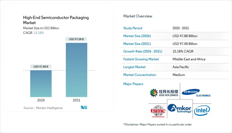
预计到 2026 年,高阶半导体封装市场规模将达到 478.8 亿美元,高于 2025 年的 415.7 亿美元。
预计到 2031 年,该产业规模将达到 970.8 亿美元,2026 年至 2031 年的复合年增长率为 15.18%。
大量资本流入异质整合领域、人工智慧加速器需求激增以及基板技术的创新共同支撑着强劲的成长势头。垂直代工一体化加剧了传统外包组装和测试 (OSAT) 供应商的竞争压力,同时也缩短了人工智慧晶片的上市时间。智慧型手机和汽车系统晶片(SoC) 供应商向 5 奈米及以下过程的转型,推动了对扇出型和硅中介层平台的需求成长。从美国的《晶片整合与保护法案》(CHIPS Act) 到欧洲的 APECS 中心,一系列区域性政策奖励正在重塑区域供应链结构,并鼓励跨国公司实现先进封装布局的多元化。同时,基板短缺和热密度限制制约了近期产能扩张,但也为能够缓解这些瓶颈的设备製造商和材料专家创造了机会。
全球高端半导体封装市场趋势与洞察
对人工智慧/机器学习加速器的需求不断增长
超大规模资料中心营运商正在向多晶片AI处理器转型,这些处理器将功耗超过1000W的运算单元与堆迭式高频宽记忆体相结合,对高阶半导体封装市场的先进温度控管和供电提出了前所未有的要求。晶圆级晶片封装(CoWoS)和类似中介层平台的产能仍然紧张,使得封装交付前置作业时间成为AI产品发布的关键环节。代工厂正在利用系统级晶圆(SoC)概念,承诺提供比现有GPU高10倍的记忆体频宽,这进一步加剧了散热设计的挑战。掌握了翘曲控制、微凸块可靠性和液冷基板技术的供应商正在获得定价权,使超大规模资料中心业者能够按时完成部署。因此,系统架构师现在将封装能力视为决定AI训练成本和所需时间的关键因素。
向智慧型手机先进製程的过渡
随着高阶智慧型手机晶片製造商向3nm和2nm製程节点过渡,晶圆成本的上升迫使扇出型晶圆层次电子构装和嵌入式桥接封装技术同步发展,以在成本限制内实现高性能。受江森自控等公司斥资6.24亿美元扩建产能的推动,中国智慧型手机製造商正加速采用国内OSAT服务,以实现价值链在地化并分散地缘政治风险。更小製程节点带来的功耗控制提升,意味着更长的电池续航时间和更丰富的设备端AI体验。然而,较小的间距需要小于2µm的线间距和超薄介电层的线路重布。在聚合物化学和电浆蚀刻技术方面不断创新的设备供应商,正透过实现这些更精细结构的高产量比率而获得竞争优势。
资本密集度提高
预计到2023年,产业资本密集度将从2015年的18%上升至30%,并持续高于30%,因为下一代封装生产线需要相容于极微影术的无尘室和后端设备,这些设备的成本高达数亿美元。中型OSAT公司正面临财务压力,这促使它们进行整合,并与资金雄厚的代工厂成立合资企业。如今,资本支出已与前端晶圆厂的支出不相上下,预计到2033年,整个产业的资本支出将超过4,600亿美元。即使是像ASMPT这样的大型设备製造商,也报告称其2024年的收入下降了10%,凸显了资本密集型週期固有的波动性。从长远来看,只有那些拥有地域多元化营运、规模优势和差异化製程智慧财产权的公司,才能在各个技术节点上持续进行投资。
细分市场分析
到2025年,2.5D中介层将占据高端半导体封装市场最大的份额,因为设计公司优先考虑的是大规模生产中已验证的产量比率和可製造性。这项技术将频宽晶粒与HBM晶粒融合在一起,使GPU和FPGA在适中的热负载下能够实现数太比特每秒的Terabit。同时,规模较小的3D系统晶片)市场预计将以16.15%的复合年增长率快速成长,这主要得益于云端和边缘设备中人工智慧推理应用场景的推动,这些场景需要将逻辑和记忆体堆迭共置。随着这些架构的日趋成熟,供应商正在优化晶粒通讯协定以降低垂直讯号传输延迟,从而加速其普及应用。
虽然中介层需求提高了基板供应商的收入可见性,但ABF(整合基板)前置作业时间风险的增加推动了人们对玻璃基和硅基中介层的兴趣。同时,3D堆迭式记忆体封装扩大了高频宽记忆体供应商的可寻址范围,增强了规模经济效益。诸如Intel EMIB之类的嵌入式桥接方案无需使用复杂的完整中介层即可实现小于55µm的晶片晶粒,为异构整合提供了低成本的切入点。在该细分市场的高端半导体封装领域,製程控制创新,特别是混合键结定位精度,仍是关键的差异化因素。
到2025年,覆晶球栅阵列(FBGA)将占据高阶半导体封装市场42.65%的份额,这主要得益于其成熟的製造基础和久经考验的可靠性指标。伺服器CPU和GPU晶片的持续成长将支撑其产量,即便其他平台不断涌现。面板级封装(PLP)到2031年将以16.32%的复合年增长率增长,因为更大的基板尺寸能够实现更高的单晶粒数量,从而降低移动和物联网SoC的单位成本。三星的试验生产线已经能够处理600毫米的玻璃面板,超过了其300毫米晶圆的产能,并对传统晶圆层次电子构装的经济性构成了威胁。
晶片级封装 (PLP) 的应用受到边缘翘曲和晶粒放置精度等挑战的限制,迫使供应商改进真空吸盘和视觉对准系统。系统级封装 (SiP) 解决方案正扩展到汽车雷达模组领域,透过整合天线和电源管理 IC 来缩小基板面积。在行动装置领域,晶圆级晶片级封装 (WL-CSP) 满足了 Z 轴高度要求和成本目标,从而维持了市场需求。随着高端半导体封装市场的不断发展,製造商越来越多地采用混合平台晶圆厂来满足每种设计的成本、性能和可靠性要求。
这份高阶半导体封装报告按技术(例如,3D系统晶片、3D堆迭记忆体)、封装平台(例如,覆晶球栅阵列、晶圆级晶片封装)、装置节点(例如,3nm以下、4-5nm)、最终用户(例如,家用电子电器、通讯和5G基础设施)以及地区进行细分。市场预测以美元计价。
区域分析
到2025年,亚太地区将占据高阶半导体封装市场58.85%的份额,这主要得益于台湾在晶圆代工领域的主导地位、韩国在记忆体技术方面的专长以及中国OSAT(外包组装、测试和封装)基础设施的快速发展。台积电、日月光和星辉半导体正将其后端生产线与前端晶圆厂毗邻而建,从而缩短生产週期并降低物流成本。同时,北京的优惠政策培育了国内产业生态系统,中国的目标是到2030年实现国内封装产能占全球38%的份额,但出口管制政策增加了地缘政治的不确定性。
北美正着力发展高价值人工智慧和国防级封装技术,其中520亿美元的《晶片法案》(CHIPS Act)资金支持了安姆科(Amcor)位于亚利桑那州价值20亿美元的工厂以及英特尔位于俄亥俄州的封装超级基地。该地区设备和材料供应商的高度集中,使得下一代技术的快速原型开发成为可能。欧洲则致力于策略自主,并已开发出耗资7.3亿欧元的APECS和8.3亿欧元的FAMES开放式原型生产线,为中小企业提供价格合理的生产空间,并培育出覆盖整个欧洲大陆的晶片生态系统。
预计到2031年,中东和非洲地区的复合年增长率将达到18.05%,这主要得益于主权财富基金对电信基础设施部署和半导体中心的投资。阿联酋等国正与全球OSAT(合约组装、测试和组装)公司合作,共同出资建设试点生产线,以满足该地区对边缘人工智慧模组的需求。南美洲虽然仍处于发展阶段,但巴西家用电子电器的契约製造正在推动对在地化测试和成品加工服务的需求成长。这种地域格局凸显了企业发展思维的转变,即从单纯的成本边际收益转向对韧性和国家安全的考量。
其他福利:
- Excel格式的市场预测(ME)表
- 3个月的分析师支持
目录
第一章 引言
- 研究假设和市场定义
- 调查范围
第二章调查方法
第三章执行摘要
第四章 市场情势
- 市场概览
- 市场驱动因素
- 对人工智慧/机器学习加速器的需求不断增长
- 智慧型手机向高阶处理节点的迁移
- IDM/OSAT异质整合蓝图
- 晶片组在低地球轨道卫星有效载荷中的应用
- 用于高效能运算的晶片-晶圆-基板(CoWoS-R)光刻掩模的生长
- 欧洲政府资助的「超越摩尔定律」试点生产线
- 市场限制
- 资本密集度提高
- 5奈米製程之后,产量比率管理变得更加复杂。
- 有机中介体基板供应瓶颈
- 3D-SoC堆迭结构中散热不均匀
- 产业价值链分析
- 监管环境
- 技术展望
- 波特五力分析
- 供应商的议价能力
- 买方的议价能力
- 新进入者的威胁
- 替代品的威胁
- 竞争程度
- 宏观经济影响评估
第五章 市场规模与成长预测
- 透过技术
- 3D系统晶片(3D-SoC)
- 3D堆迭式记忆体(HBM、HBM-PIM)
- 2.5D 中介层
- 超高密度扇出 (UHD-FO)
- 嵌入式硅桥/EMIB
- 透过包装平台
- 覆晶球栅阵列(FC-BGA)
- 晶圆级晶片封装(WLCSP)
- 面板级包装(PLP)
- 系统级封装(SiP)
- 按设备节点
- 3奈米或更小
- 4-5 nm
- 6-7 nm
- 10奈米或更大
- 最终用户
- 家用电子电器
- 电信和5G基础设施
- 汽车和ADAS
- 航太/国防
- 医疗设备
- 按地区
- 北美洲
- 我们
- 加拿大
- 墨西哥
- 南美洲
- 巴西
- 阿根廷
- 哥伦比亚
- 南美洲其他地区
- 欧洲
- 英国
- 德国
- 法国
- 义大利
- 西班牙
- 其他欧洲地区
- 亚太地区
- 中国
- 日本
- 韩国
- 印度
- 亚太其他地区
- 中东和非洲
- 中东
- 沙乌地阿拉伯
- 阿拉伯聯合大公国
- 其他中东地区
- 非洲
- 南非
- 埃及
- 其他非洲地区
- 中东
- 北美洲
第六章 竞争情势
- 市场集中度
- 策略趋势
- 市占率分析
- 公司简介
- Advanced Semiconductor Engineering Inc.(ASE Technology Holding Co., Ltd.)
- Amkor Technology, Inc.
- Intel Corporation
- Taiwan Semiconductor Manufacturing Company Limited(TSMC)
- Samsung Electronics Co., Ltd.
- JCET Group Co., Ltd.
- Siliconware Precision Industries Co., Ltd.(SPIL)
- Powertech Technology Inc.(PTI)
- TongFu Microelectronics Co., Ltd.
- Fujitsu Limited
- Texas Instruments Incorporated
- United Microelectronics Corporation(UMC)
- STATS ChipPAC Pte Ltd.
- Hiksemi Microelectronics Co., Ltd.
- Nanium SA(Infineon Backend)
- Chip MOS Technologies Inc.
- Taiwan Advanced Packaging Corporation(TAPC)
- Unimicron Technology Corp.
- Shinko Electric Industries Co., Ltd.
- Kyocera Corporation(AVX)
第七章 市场机会与未来展望
The high-end semiconductor packaging market size in 2026 is estimated at USD 47.88 billion, growing from 2025 value of USD 41.57 billion with 2031 projections showing USD 97.08 billion, growing at 15.18% CAGR over 2026-2031.
Robust capital flows toward heterogeneous integration, surging AI accelerator demand, and substrate innovations together reinforce a strong growth trajectory. Foundry vertical integration amplifies competitive pressure on traditional outsourced assembly and test (OSAT) vendors while improving time-to-market for AI chips. Sub-5 nm migration by smartphone and automotive system-on-chip (SoC) suppliers fuels incremental volume for fan-out and silicon interposer platforms. Regional policy incentives, from the U.S. CHIPS Act to Europe's APECS hub, are reshaping supply-chain geography, prompting multinational firms to diversify advanced packaging footprints. Meanwhile, substrate shortages and thermal-density limits temper near-term capacity ramps but simultaneously open opportunities for toolmakers and materials specialists that mitigate these bottlenecks.
Global High-End Semiconductor Packaging Market Trends and Insights
Rising Demand for AI/ML Accelerators
Hyperscale data-center operators pivot to multi-die AI processors that fuse >1,000 W compute tiles with stacked high-bandwidth memory, driving an unprecedented requirement for advanced thermal and power delivery inside the high-end semiconductor packaging market. Capacity for CoWoS and similar interposer platforms remains tight, elevating packaging lead-times to critical-path status for AI product launches. Foundries leveraging system-on-wafer concepts promise 10X memory bandwidth over current GPUs, further intensifying thermal engineering challenges. Vendors that master warpage control, micro-bump reliability, and liquid-coolable substrates gain pricing power as they enable hyperscalers to meet rollout schedules. Consequently, packaging capability is now viewed by system architects as a primary determinant of AI training cost and time.
Smartphone Migration to Advanced Nodes
Premium smartphone chipmakers are transitioning toward 3 nm and 2 nm production nodes, but rising wafer cost forces parallel advances in fan-out wafer-level and embedded bridge packaging to deliver performance within cost envelopes. Chinese handset brands accelerate adoption of domestic OSAT services following capacity acquisitions such as JCET's USD 624 million expansion, localizing value chains, and balancing geopolitical risk. Power-budget gains derived from finer nodes translate into longer battery life and richer on-device AI experiences; however, the tighter pitch requires redistribution layers with sub-2 µm line-and-space and ultra-thin dielectrics. Equipment suppliers innovating in polymer chemistries and plasma etch achieve a competitive advantage by enabling high volume yields at these geometries.
Escalating Capital Intensity
Industry capital intensity climbed from 18% in 2015 to 30% in 2023 and is expected to remain above 30% as next-generation packaging lines require EUV-litho-grade cleanrooms and back-end tools costing hundreds of millions of dollars. Mid-tier OSATs face balance-sheet stress, prompting consolidation or joint ventures with foundries wielding deep pockets. Equipment expenditures now rival front-end fab outlays, with projections exceeding USD 460 billion industry-wide by 2033. Even leading toolmakers such as ASMPT reported 10% revenue contraction in 2024, underscoring the volatility inherent in capex-heavy cycles. In the long term, only geographically diversified players with scale and differentiated process IP can fund successive technology nodes.
Other drivers and restraints analyzed in the detailed report include:
- Heterogeneous Integration Road-maps of IDMs/OSATs
- Growth of CoWoS-R for HPC Reticles
- Yield Management Complexity Beyond 5 nm
For complete list of drivers and restraints, kindly check the Table Of Contents.
Segment Analysis
2.5 D interposers captured the largest slice of the high-end semiconductor packaging market in 2025 as design houses prioritized proven yield and manufacturability at volume. The technology fuses logic and HBM dies with a moderate thermal penalty, supporting multi-terabit per second bandwidth in GPUs and FPGAs. By contrast, the 3D System-on-Chip segment, though smaller, is projected to clock the fastest 16.15% CAGR, underpinned by AI inference use cases in cloud and edge appliances that require co-located logic and memory stacks. As these architectures mature, vendors are optimizing die-to-die communication protocols to alleviate vertical signaling latency, accelerating broader adoption.
Interposer demand boosts revenue visibility for substrate suppliers, but mounting ABF lead-time risk has propelled interest in glass and silicon-based interposers. Meanwhile, 3D stacked-memory packages broaden the addressable base for high-bandwidth memory vendors, reinforcing scale economies. Embedded-bridge methods like Intel EMIB achieve die-to-die pitch <55 µm without full interposer complexity, offering a lower-cost entry point for heterogeneous integration. Within the high-end semiconductor packaging market size for this segment, process control innovations-especially hybrid bonding align accuracy-remain primary differentiators.
Flip-chip ball-grid-array held 42.65% of the high-end semiconductor packaging market share in 2025, thanks to an entrenched manufacturing base and well-documented reliability metrics. Continued growth in server CPUs and GPU tiles sustains volumes even as alternative platforms emerge. Panel-level packaging (PLP) rides a 16.32% CAGR through 2031 because larger substrate form factors permit more dies per carrier, lowering cost per unit for mobile and IoT SoCs. Samsung's pilot lines already process 600 mm glass panels, outpacing 300 mm wafer throughput and threatening traditional wafer-level economics.
PLP adoption is constrained by edge-warpage and die-placement accuracy challenges, compelling equipment vendors to refine vacuum-chuck and vision-alignment systems. System-in-Package solutions extend to automotive radar modules, integrating antennas and power management ICs to trim board area. In mobile devices, wafer-level chip-scale packages meet z-height mandates and cost goals, preserving demand momentum. As the high-end semiconductor packaging market evolves, manufacturers increasingly run mixed-platform fabs to align each design's cost, performance, and reliability envelope.
The High-End Semiconductor Packaging Report is Segmented by Technology (3D System-On-Chip, 3D Stacked Memory, and More), Packaging Platform (Flip-Chip Ball-Grid-Array, Wafer-Level Chip-Scale Package, and More), Device Node (Less Than or Equal To 3 Nm, 4-5 Nm, and More), End User (Consumer Electronics, Telecom and 5G Infrastructure, and More), and Geography. The Market Forecasts are Provided in Terms of Value (USD).
Geography Analysis
Asia-Pacific controlled 58.85% of the high-end semiconductor packaging market in 2025, anchored by Taiwan's foundry leadership, South Korea's memory expertise, and China's rapid OSAT build-out. TSMC, ASE Technology, and SPIL co-locate back-end lines next to front-end fabs, compressing cycle time and lowering logistic overhead. Simultaneously, Beijing's incentives foster a domestic ecosystem targeting 38% of global installed packaging capacity by 2030, though export-control policies add geopolitical uncertainty.
North America concentrates on high-value AI and defense-grade packages, buoyed by USD 52 billion CHIPS funding that subsidizes Amkor's USD 2 billion Arizona facility and Intel's Ohio packaging megasite. The region also houses a dense cluster of equipment and materials suppliers, allowing rapid prototyping for next-generation technologies. Europe pursues strategic autonomy through €730 million APECS and €830 million FAMES open-access pilot lines, giving SMEs affordable fabrication slots and seeding a continental chiplet ecosystem.
The Middle East and Africa chart an 18.05% CAGR through 2031, propelled by telecom infrastructure rollouts and sovereign funds investing in semiconductor hubs. Countries such as the United Arab Emirates partner with global OSATs to co-finance pilot lines, targeting regional demand for edge AI modules. South America remains nascent but benefits from consumer-electronics contract manufacturing in Brazil, generating incremental demand for localized test and finish services. The geographic mosaic underscores a shift from pure cost arbitrage toward resilience and national-security considerations.
- Advanced Semiconductor Engineering Inc. (ASE Technology Holding Co., Ltd.)
- Amkor Technology, Inc.
- Intel Corporation
- Taiwan Semiconductor Manufacturing Company Limited (TSMC)
- Samsung Electronics Co., Ltd.
- JCET Group Co., Ltd.
- Siliconware Precision Industries Co., Ltd. (SPIL)
- Powertech Technology Inc. (PTI)
- TongFu Microelectronics Co., Ltd.
- Fujitsu Limited
- Texas Instruments Incorporated
- United Microelectronics Corporation (UMC)
- STATS ChipPAC Pte Ltd.
- Hiksemi Microelectronics Co., Ltd.
- Nanium S.A. (Infineon Backend)
- Chip MOS Technologies Inc.
- Taiwan Advanced Packaging Corporation (TAPC)
- Unimicron Technology Corp.
- Shinko Electric Industries Co., Ltd.
- Kyocera Corporation (AVX)
Additional Benefits:
- The market estimate (ME) sheet in Excel format
- 3 months of analyst support
TABLE OF CONTENTS
1 INTRODUCTION
- 1.1 Study Assumptions and Market Definition
- 1.2 Scope of the Study
2 RESEARCH METHODOLOGY
3 EXECUTIVE SUMMARY
4 MARKET LANDSCAPE
- 4.1 Market Overview
- 4.2 Market Drivers
- 4.2.1 Rising demand for AI/ML accelerators
- 4.2.2 Smartphone migration to advanced nodes
- 4.2.3 Heterogeneous integration road-maps of IDMs/OSATs
- 4.2.4 Adoption of chip-lets for LEO satellite payloads
- 4.2.5 Growth of Chip-on-Wafer-on-Substrate (CoWoS-R) for HPC reticles
- 4.2.6 Government-funded 'More-than-Moore' pilot lines in Europe
- 4.3 Market Restraints
- 4.3.1 Escalating capital intensity
- 4.3.2 Yield management complexity beyond 5 nm
- 4.3.3 Sub-strate supply bottlenecks for organic interposers
- 4.3.4 Non-uniform thermal dissipation in 3D-SoC stacks
- 4.4 Industry Value Chain Analysis
- 4.5 Regulatory Landscape
- 4.6 Technological Outlook
- 4.7 Porter's Five Forces Analysis
- 4.7.1 Bargaining Power of Suppliers
- 4.7.2 Bargaining Power of Buyers
- 4.7.3 Threat of New Entrants
- 4.7.4 Threat of Substitutes
- 4.7.5 Degree of Competition
- 4.8 Assessment of Macroeconomic Impact
5 MARKET SIZE AND GROWTH FORECASTS (VALUE)
- 5.1 By Technology
- 5.1.1 3D System-on-Chip (3D-SoC)
- 5.1.2 3D Stacked Memory (HBM, HBM-PIM)
- 5.1.3 2.5D Interposers
- 5.1.4 Ultra-High-Density Fan-Out (UHD-FO)
- 5.1.5 Embedded Si Bridge / EMIB
- 5.2 By Packaging Platform
- 5.2.1 Flip-Chip Ball-Grid-Array (FC-BGA)
- 5.2.2 Wafer-Level Chip-Scale Package (WLCSP)
- 5.2.3 Panel-Level Packaging (PLP)
- 5.2.4 System-in-Package (SiP)
- 5.3 By Device Node
- 5.3.1 Less than or Equal to 3 nm
- 5.3.2 4-5 nm
- 5.3.3 6-7 nm
- 5.3.4 Greater than or Equal to 10 nm
- 5.4 By End User
- 5.4.1 Consumer Electronics
- 5.4.2 Telecom and 5G Infrastructure
- 5.4.3 Automotive and ADAS
- 5.4.4 Aerospace and Defense
- 5.4.5 Medical Devices
- 5.5 By Geography
- 5.5.1 North America
- 5.5.1.1 United States
- 5.5.1.2 Canada
- 5.5.1.3 Mexico
- 5.5.2 South America
- 5.5.2.1 Brazil
- 5.5.2.2 Argentina
- 5.5.2.3 Colombia
- 5.5.2.4 Rest of South America
- 5.5.3 Europe
- 5.5.3.1 United Kingdom
- 5.5.3.2 Germany
- 5.5.3.3 France
- 5.5.3.4 Italy
- 5.5.3.5 Spain
- 5.5.3.6 Rest of Europe
- 5.5.4 Asia-Pacific
- 5.5.4.1 China
- 5.5.4.2 Japan
- 5.5.4.3 South Korea
- 5.5.4.4 India
- 5.5.4.5 Rest of Asia-Pacific
- 5.5.5 Middle East and Africa
- 5.5.5.1 Middle East
- 5.5.5.1.1 Saudi Arabia
- 5.5.5.1.2 United Arab Emirates
- 5.5.5.1.3 Rest of Middle East
- 5.5.5.2 Africa
- 5.5.5.2.1 South Africa
- 5.5.5.2.2 Egypt
- 5.5.5.2.3 Rest of Africa
- 5.5.5.1 Middle East
- 5.5.1 North America
6 COMPETITIVE LANDSCAPE
- 6.1 Market Concentration
- 6.2 Strategic Moves
- 6.3 Market Share Analysis
- 6.4 Company Profiles (includes Global level Overview, Market level overview, Core Segments, Financials as available, Strategic Information, Market Rank/Share, Products and Services, Recent Developments)
- 6.4.1 Advanced Semiconductor Engineering Inc. (ASE Technology Holding Co., Ltd.)
- 6.4.2 Amkor Technology, Inc.
- 6.4.3 Intel Corporation
- 6.4.4 Taiwan Semiconductor Manufacturing Company Limited (TSMC)
- 6.4.5 Samsung Electronics Co., Ltd.
- 6.4.6 JCET Group Co., Ltd.
- 6.4.7 Siliconware Precision Industries Co., Ltd. (SPIL)
- 6.4.8 Powertech Technology Inc. (PTI)
- 6.4.9 TongFu Microelectronics Co., Ltd.
- 6.4.10 Fujitsu Limited
- 6.4.11 Texas Instruments Incorporated
- 6.4.12 United Microelectronics Corporation (UMC)
- 6.4.13 STATS ChipPAC Pte Ltd.
- 6.4.14 Hiksemi Microelectronics Co., Ltd.
- 6.4.15 Nanium S.A. (Infineon Backend)
- 6.4.16 Chip MOS Technologies Inc.
- 6.4.17 Taiwan Advanced Packaging Corporation (TAPC)
- 6.4.18 Unimicron Technology Corp.
- 6.4.19 Shinko Electric Industries Co., Ltd.
- 6.4.20 Kyocera Corporation (AVX)
7 MARKET OPPORTUNITIES AND FUTURE OUTLOOK
- 7.1 White-space and Unmet-Need Assessment
 2026年全球半导体封装市场报告
 3-D TSV:关键问题洞察与市场分析
 高密度封装(MCM、MCP、SIP、3D-TSV):市场分析与技术趋势
 全球防静电载带捲市场(按载带类型、材料、胶带材料成分、胶带层数和最终用途产业划分)预测(2026-2032年)导线架固定胶带市场(按黏合剂类型、背衬材料、胶带宽度、胶带厚度、应用、最终用途行业和销售管道),全球预测,2026-2032年
 MEMS封装焊料市场规模、份额和成长分析:按焊料类型、产品形式、应用、封装类型、最终用户和地区划分 - 2026-2033年产业预测
 先进半导体封装市场分析及预测(至2035年):依类型、产品类型、服务、技术、应用、材料类型、装置、製程、最终用户及功能划分半导体原型製作及封装市场分析及预测(至2035年):依类型、产品类型、服务、技术、应用、材料类型、组件、製程、最终用户、设备划分半导体封装市场分析及预测(至2035年):依类型、产品类型、技术、应用、材料类型、装置、製程、最终用户、功能、设备划分2026年全球四方扁平包装市场报告