|
年间契约型资讯服务
商品编码
1413686
先进封装专利监测服务Advanced Packaging Patent Monitoring Service |
|||||||
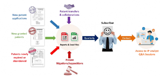
该服务提供半导体先进封装领域专利活动的最新数据(新专利申请数量、获得的新专利数量、专利到期/放弃数量、专利转让数量以及专利诉讼的最新趋势/反对)。等)。
服务主要特点
该报告提供最新的 Excel 资料库(按季度):
- 新专利申请数量
- 取得新专利数量
- 专利到期/放弃的数量
- 智慧财产权 (IP) 转让(重新分配、授权)和合作(联合申请)数量
- 专利诉讼和异议
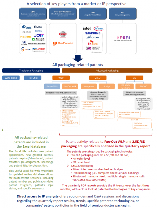
- 依封装技术分类的专利:扇出封装(晶圆级、面板级)、2.5D 和 3D 封装(中介层、桥接器、混合键结、3D 堆迭记忆体)
每个季度,您都会收到以下 PDF 报告:
- 关键数据(季度)
- 透过图表和评论介绍专利状态的趋势
- 各大知识产权公司及技术特写
每年 100 小时与 IP 分析师接触:
- 与智慧财产权分析师就季度分析结果、市场趋势、分析内容、具体专利技术以及公司在先进封装领域的智慧财产权组合进行问答和讨论。
2.5D/3D 堆迭和扇出 WLP 是满足半导体封装市场需求的有前途的解决方案。监控主要半导体封装公司的专利活动和智慧财产权策略至关重要。
在半导体产业,对单一包装中更多运算能力和记忆体的需求不断增长,以缩小外形尺寸并提高产品效能。然而,随着节点达到其发展极限,摩尔定律变得越来越难以实现。因此,晶片小型化的进程正在放缓。2.5D和3D堆迭以及扇出晶圆级封装等先进封装技术已成为满足半导体产业需求的重要解决方案。这些新方法能够将多个晶片整合到单一封装中,并有可能结合成熟和先进的节点,取代主导的倒装晶片 (FC) 和引线键合 (WB) 互补技术。这些先进封装技术的路线图具有挑战性,包括高密度扇出(HD FO) 重新分布层(RDL)、高密度输入/输出互连(I/O) 以及硅中介层、嵌入式桥接器和混合键合对先进互连技术(例如小晶片方法)的需求正在加剧供应链竞争。2.5/3D 封装市场具有最高的成长潜力,由于小晶片 3D 整合混合键合的普及,3D SoC 技术成长最快。在扇出 WLP 产业中,超高密度扇出 (UHD FO) 正在经历最高的成长,因为与硅中介层相比,它已成为一种经济高效的解决方案。半导体封装主要由ASE/SPIL、Amkor 和 JCET等 OSAT 完成,它们继续在该领域发挥重要作用。然而,TSMC、Samsung和Intel正在开发创新的 2.5D/3D 封装解决方案,例如硅中介层、嵌入式桥和混合结。透过提供先进的后端解决方案并利用前端功能,这些公司有望影响该领域未来的技术和智慧财产权 (IP) 发展。
在此背景下,监控主要公司的专利活动和智慧财产权(IP)策略至关重要。这些知识可以帮助您了解竞争对手的研发路线图和策略、评估风险并发现商机。我们的服务支援 TSMC、Intel、Samsung、Amkor、ASE、SPIL、JCET、Deca、Nepes、Powertech (PTI)、SJSemi、Tongfu (TFME)、Huatian、Infineon、Micron、SK Hynix、YMTC、GlobalFoundries、Xperi/Adeia 能够定期了解各大公司的智慧财产权活动,例如
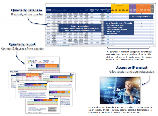
我们的服务利用每季更新一次的 Excel 资料库,让您能够从季度分析报告以及与分析师的直接互动中受益。
专利监测服务优势
您可以监控竞争对手的知识产权活动和未来意图。
我们的服务使您能够了解竞争对手目前的专利活动、智慧财产权动态、专利转移(包括收购和授权)、专利诉讼、技术开发和研发策略。此外,可以在早期发现进入该业务领域的新进入者。
我们了解最新的技术趋势并保持领先地位。
追踪最近的专利申请趋势可以让您追踪您所在领域的最新创新。获取已提交发明的详细资讯并追踪技术发展。受新技术解决方案的启发,研究和开发活动可能会得到改善。
您可以阻止註册对您的业务有害的智慧财产权。
在授予专有权之前获取有关已提交专利申请的信息,并迅速采取行动,防止可能对您的业务产生负面影响的知识产权註册。
快速回应违规行为并降低法律风险。
监控新颁发的专利,以确保您的产品和工艺不受专利保护,并且您可以安全地製造它们,而不会侵犯他人拥有的有效智慧财产权。您可以定期评估您的销售和使用的商业自由度。
利用免费技术降低研发专案的风险。
透过追踪过期和废弃的专利,您可以识别公共领域中可以安全用于您的开发的发明。
了解竞争对手目前的知识产权趋势和策略。
每个季度,我们都会提供近三个月知识产权动态特写,重点关注主要知识产权企业和主要专利技术。突出显示了关键专利申请人及其发明、被阻止的专利、有前途的专利以及新到期或放弃的关键专利。
接触知识产权分析师。
您将有机会透过电话或电子邮件与分析师直接互动,并透过问答和公开讨论(每年 100 小时)获取有关特定专利技术或公司智慧财产权组合的具体资讯。
目录(样本)
简介/研究法
主要趋势
- 近10年专利公开数量变化
- 扇出 (FO) 封装
- 硅中介层
- 内建互连桥
- 混合连接
- 3D堆迭内存
市场概况(季度)
- 本季的主要事实
- 本季新发布/授予的同族专利
- 本季度过期或被放弃的专利
- 重大智慧财产权合作(联合申请专利)
- 主要智慧财产权转让(专利权属变更)
- 在美国发起和完成的智慧财产权诉讼数量
- 向 EP(欧洲专利局)提出的新异议数量
本季各公司的知识产权活动
专业铸造厂
- TSMC
- GlobalFoundries
OSAT
- Amkor
- ASE
- SPIL
- JCET
- Nepes
- Powertech
- Technology
- Deca
- Huatian
- Technology
- SJSemi
- Tongfu
- Microelectronics
IDM
- Samsung
- Infineon
- Intel
- Micron
- SK
- Hynix
- YMTC
NPE
- Xperi
附录
Get up-to-date data on Advanced Semiconductor Packaging patent activity: New patent applications, patents newly granted, expired or abandoned patents, latest patent transfers, patent litigations and oppositions.
Key Features of the service
Every quarter an up-to-date Excel database including:
- New patents applications
- Patent applications newly granted
- Expired or abandoned patents
- Transfer of IP rights (re-assignment, licensing) and IP collaborations (co-fillings)
- Patent litigations and oppositions.
- Patents categorized by packaging technologies: Fan-Out packaging (wafer level, panel level), 2.5D & 3D packaging (interposer, bridge, hybrid bonding, 3D-stacked memory)
Every quarter a PDF report including:
- Key fact & figures of the quarter
- Graphs & comments covering the patent landscape evolutions
- A close look at the key IP players and technologies
Access to an IP analyst for 100 hours per year:
- Q&A sessions and discussions with our IP analysts regarding quarterly report results, trends, analyses, specific patented technologies, or companies' IP portfolios in the field of Advanced Packaging.
2.5D/3D stacking and fan-out WLP are promising solutions to meet the needs of the semiconductor packaging market. It is crucial to monitor patent activity and IP strategies of key semiconductor packaging players
In the semiconductor industry, there is a growing demand for integrating more compute and memory within a single package in order to achieve smaller form factors and improve product performance. However, Moore's Law becomes increasingly difficult to achieve as node advancement reaches its limits. As a result, the process of chip miniaturization has been slowing down. Advanced packaging techniques, such as 2.5D & 3D stacking, and fan-out wafer level packaging, have emerged as crucial solutions to meet the needs of the semiconductor industry. These new approaches allow for the integration of multiple dies into a single package, with the possibility of combining mature and advanced nodes, and they have supplemented the dominant flip-chip (FC) and wire-bond (WB) technologies. The roadmap for these advanced packaging technologies is challenging and the supply chain is becoming increasingly competitive, with the demand for high-density fan-out (HD FO) redistribution layers (RDLs), high-density input/output interconnections (I/O), and advanced interconnect technologies such as silicon interposer, embedded bridge, hybrid bonding, and chiplets approach. The market for 2.5/3D packaging shows the most potential for growth, with 3D SoC technology growing the most driven by the increasing popularity of hybrid bonding for chiplets 3D integration. In the fan-out WLP industry, the segment experiencing the highest growth is the ultra-high density fan-out (UHD FO), which has emerged as a more cost-effective solution compared to silicon interposers. Semiconductor packaging was primarily performed by OSATs such as ASE/SPIL, Amkor, JCET, etc. and they continue to play an important role in this field. However, it is TSMC, Samsung and Intel that have been developing innovative 2.5D/3D packaging solutions such as silicon interposer, embedded bridge, and hybrid bonding. By offering advanced back-end solutions and using their front-end capabilities, these companies poised to influence future technology and intellectual property (IP) developments in this area.
In this context, it is crucial to monitor patent activity and intellectual property (IP) strategies of key players. Such knowledge can assist in understanding your competitors' R&D roadmap and strategies, evaluate the risks, and detect business opportunities. The Advanced Packaging Patent Monitor gives periodic insights on the IP activity of a selection of key companies: TSMC, Intel, Samsung, Amkor, ASE, SPIL, JCET, Deca, Nepes, Powertech (PTI), SJSemi, Tongfu (TFME), Huatian, Infineon, Micron, SK Hynix, YMTC, GlobalFoundries, and Xperi/Adeia.

The Advanced Packaging patent monitoring service allows you to take advantage of a quarterly-updated Excel database and benefit from both quarterly analysis reports and direct interaction with our analysts.

Benefits of the patent monitoring service
Keep a watch on your competitors' IP activities and their future intentions.
With the help of the patent monitoring service, you will be aware of your competitors' current patenting activities, their IP dynamics, patent transfers including acquisitions and licenses, patent litigation, technology development and R&D strategies. You will also be able to early detect new entrants in your business area.
Keep track of the latest technology developments and be ahead of technology trends.
By keeping note of any recent patent filings, you can track the newest innovations in the field. You will get details on claimed inventions and you can follow technology developments. New technical solutions could inspire and improve your R&D activity.
Prevent registration of IP rights that may be harmful to your business.
You will obtain information on patent applications filed even before exclusive rights have been granted and you can react in time to prevent registration of IP rights that may be harmful to your business.
React in time to infringements and mitigate legal risks.
Monitoring newly-issued patents allows you to regularly assess your freedom-to-operate, ensuring your products or processes are not covered by patents, and thus that they can be manufactured, sold or used safely without infringing valid IP rights owned by others.
Take advantage of free technologies and decrease R&D project risks.
By tracking both expired patents and abandoned patents, you will be able to identify inventions entering the public domain that you can use safely for your development.
Understand the current IP trends and IP strategy of competitors.
On a quarterly basis, the report will provide the IP trends over the three last months, with a close look to key IP players and key patented technologies. Main patent applicants and their inventions, blocking patents, promising patents and key patents newly expired or abandoned will be highlighted.
Access to the IP analyst.
Take advantage of direct interaction with our analysts by phone call and/or email and get specific input for specific patented technologies and company IP portfolios through Q&A session and open discussion (100h per year).

TABLE OF CONTENTS (SAMPLE)
INTRODUCTION METHODOLOGY
- Context
- Scope of the patent monitoring service
- Methodology and segments definition
- Companies tracked in this patent monitoring service
MAIN TRENDS
- Time evolution of patent publications over the past decade
- Fan Out packaging
- Silicon interposer
- Embedded interconnect bridge
- Hybrid bonding
- 3D stacked memories
QUARTER OVERVIEW
- Key facts of the quarter
- Patent families newly published and granted in the quarter
- Patents expired or abandoned in the quarter
- Main IP collaborations (patent co filings)
- Main IP transfers (change in patent ownership)
- US IP litigations open or closed
- New EP oppositions
PLAYERS IP ACTIVITY DURING THE QUARTER
Pure play foundries
- TSMC
- GlobalFoundries
OSATs
- Amkor
- ASE
- SPIL
- JCET
- Nepes
- Powertech
- Technology
- Deca
- Huatian
- Technology
- SJSemi
- Tongfu
- Microelectronics
IDMs
- Samsung
- Infineon
- Intel
- Micron
- SK
- Hynix
- YMTC
NPE
- Xperi


