


 |
市场调查报告书
商品编码
1721493
3D 堆迭市场机会、成长动力、产业趋势分析及 2025 - 2034 年预测3D Stacking Market Opportunity, Growth Drivers, Industry Trend Analysis, and Forecast 2025 - 2034 |
||||||
2024 年全球 3D 堆迭市场价值为 18 亿美元,预计到 2034 年将以 21.1% 的复合年增长率成长,达到 118 亿美元。这一显着增长主要归因于对消费性电子产品、高效能运算系统和先进半导体技术不断增长的需求。随着人工智慧 (AI)、机器学习和物联网 (IoT) 等资料密集型应用的不断扩展,对更快的资料处理、更高的效率和更好的电源管理的需求变得比以往任何时候都更加重要。 3D 堆迭技术越来越多地被视为半导体创新的未来,它使设备製造商能够透过在紧凑的空间内整合多个功能层(例如逻辑、记忆体和互连)来满足这些不断变化的需求。随着电子产业在不影响效能的情况下不断朝向小型化发展,3D 堆迭提供了实现更高吞吐量、更低延迟和卓越热管理的理想途径。从智慧型手机和穿戴式装置到资料中心处理器和自动驾驶汽车,这项技术的应用范围正在迅速扩大。基于小晶片的设计和异质整合的采用进一步推动了该市场的发展势头,为跨行业的特定用例客製化解决方案提供了灵活性。
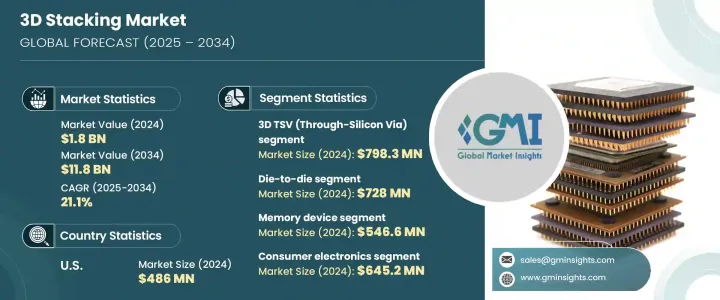
3D堆迭技术依互连方式可分为3D混合键结、3D硅通孔(TSV)、单晶片3D整合等。其中,3D TSV 部分在 2024 年创造了 7.983 亿美元的收入。由于对支援资料中心、HPC 平台和自主系统效能要求的高速、低延迟记忆体介面的需求不断增长,该部分正在经历强劲增长。 5G 网路的推出和智慧型装置的普及也加剧了对能够管理大量即时资料处理的节能、紧凑晶片架构的需求。
| 市场范围 | |
|---|---|
| 起始年份 | 2024 |
| 预测年份 | 2025-2034 |
| 起始值 | 18亿美元 |
| 预测值 | 118亿美元 |
| 复合年增长率 | 21.1% |
市场进一步依互连技术细分,包括晶片到晶圆、晶圆到晶圆、晶片到晶片、晶片到晶片和晶片到晶圆技术。 2024 年,晶片到晶片领域的价值为 7.28 亿美元。这种方法对于需要晶片之间无缝通讯的多晶片模组和基于晶片组的架构尤其重要。它在推动人工智慧加速器、云端基础设施和 HPC 处理器方面发挥关键作用,提供了更大的设计灵活性、增强的节能效果和改进的可扩展性。
2024 年,美国 3D 堆迭市场产值达 4.86 亿美元。由于对人工智慧应用、先进资料中心营运和 HPC 基础设施的投资增加,该地区正在经历大幅成长。美国半导体公司正在投入资源开发小晶片架构和基于 TSV 的设计,以突破下一代运算的效能、能源效率和可扩展性的界限。
全球 3D 堆迭市场的主要参与者包括 AMD、ASE Technology Holding、Amkor Technology、Broadcom、IBM、Intel、Graphcore、JCET Group、Marvell Technology、Micron Technology、Kioxia、NVIDIA、OmniVision Technologies、SK Hynix、Sony Semiconductor Solutions、Samsung EILlectronics、SPSPung EILlectin、Westx、Westx、Westx、Westx。这些公司正在加速晶片堆迭和互连方法的创新,以满足人工智慧、资料中心和高效能运算市场日益增长的需求。透过专注的研发和策略性投资,他们旨在提供结合了功率效率、卓越性能和架构灵活性的面向未来的半导体解决方案。
目录
第一章:方法论与范围
第二章:执行摘要
第三章:行业洞察
- 产业生态系统分析
- 产业衝击力
- 成长动力
- 对高效能运算(HPC)的需求不断增长
- 扩展人工智慧和边缘运算的应用
- 消费性电子产品的成长
- 汽车和物联网应用增加
- 记忆体和储存需求成长
- 产业陷阱与挑战
- 製造成本高且复杂
- 散热和电源管理问题
- 成长动力
- 成长潜力分析
- 监管格局
- 技术格局
- 未来市场趋势
- 差距分析
- 波特的分析
- PESTEL分析
第四章:竞争格局
- 介绍
- 公司市占率分析
- 主要市场参与者的竞争分析
- 竞争定位矩阵
- 策略仪表板
第五章:市场估计与预测:依方法,2021 年至 2034 年
- 主要趋势
- 死对死
- 晶片到晶圆
- 晶圆对晶圆
- 晶片到晶片
- 晶片到晶圆
第六章:市场估计与预测:按互连技术,2021 年至 2034 年
- 主要趋势
- 3D混合键合
- 3D TSV(硅通孔)
- 单晶片3D集成
第七章:市场估计与预测:按设备类型,2021 年至 2034 年
- 主要趋势
- 逻辑积体电路
- 成像与光电子
- 储存装置
- MEMS/感测器
- 发光二极体
- 其他(射频、光子学、类比和混合讯号以及功率装置)
第八章:市场估计与预测:按最终用途产业,2021 年至 2034 年
- 主要趋势
- 消费性电子产品
- 製造业
- 通讯(电信、资料中心和高效能运算)
- 汽车
- 医疗器材/医疗保健
- 其他(军事与国防、航空
第九章:市场估计与预测:按地区,2021 年至 2034 年
- 主要趋势
- 北美洲
- 我们
- 加拿大
- 欧洲
- 德国
- 英国
- 法国
- 西班牙
- 义大利
- 荷兰
- 亚太地区
- 中国
- 印度
- 日本
- 澳洲
- 韩国
- 拉丁美洲
- 巴西
- 墨西哥
- 阿根廷
- 中东和非洲
- 沙乌地阿拉伯
- 南非
- 阿联酋
第十章:公司简介
- AMD
- Amkor Technology
- ASE Technology Holding
- Broadcom
- Graphcore
- IBM
- Intel
- JCET Group
- Kioxia
- Marvell Technology
- Micron Technology
- NVIDIA
- OmniVision Technologies
- Samsung Electronics
- SK Hynix
- Sony Semiconductor Solutions
- SPIL
- TSMC
- Western Digital
- Xilinx
The Global 3D Stacking Market was valued at USD 1.8 billion in 2024 and is expected to grow at a CAGR of 21.1% to reach USD 11.8 billion by 2034. This remarkable growth is largely attributed to the rising demand for consumer electronics, high-performance computing systems, and advanced semiconductor technologies. As data-intensive applications such as artificial intelligence (AI), machine learning, and the Internet of Things (IoT) continue to scale, the need for faster data processing, enhanced efficiency, and improved power management becomes more critical than ever. 3D stacking technology is increasingly seen as the future of semiconductor innovation, enabling device manufacturers to meet these evolving needs by integrating multiple functional layers-such as logic, memory, and interconnects-within a compact footprint. As the electronics industry pushes toward miniaturization without compromising performance, 3D stacking provides an ideal pathway to achieve higher throughput, lower latency, and superior thermal management. From smartphones and wearables to data center processors and autonomous vehicles, the scope of applications for this technology is rapidly expanding. The adoption of chiplet-based designs and heterogeneous integration further drives this market's momentum, offering the flexibility to customize solutions for specific use cases across industries.
3D stacking technology is classified based on interconnection methods, including 3D hybrid bonding, 3D Through-Silicon Via (TSV), and monolithic 3D integration. Among these, the 3D TSV segment generated USD 798.3 million in 2024. This segment is experiencing robust growth due to rising demand for high-speed, low-latency memory interfaces that support the performance requirements of data centers, HPC platforms, and autonomous systems. The rollout of 5G networks and the proliferation of smart devices are also intensifying the need for energy-efficient and compact chip architectures that can manage vast volumes of real-time data processing.
| Market Scope | |
|---|---|
| Start Year | 2024 |
| Forecast Year | 2025-2034 |
| Start Value | $1.8 Billion |
| Forecast Value | $11.8 Billion |
| CAGR | 21.1% |
The market is further segmented by interconnect technology, including die-to-wafer, wafer-to-wafer, die-to-die, chip-to-chip, and chip-to-wafer techniques. The die-to-die segment was valued at USD 728 million in 2024. This method is especially vital for multi-chip modules and chipset-based architectures that require seamless communication between dies. It plays a key role in advancing AI accelerators, cloud infrastructure, and HPC processors, offering greater design flexibility, enhanced energy savings, and improved scalability.
United States 3D Stacking Market generated USD 486 million in 2024. The region is witnessing substantial growth owing to increased investments in AI applications, advanced data center operations, and HPC infrastructure. US-based semiconductor firms are channeling resources into developing chiplet architectures and TSV-based designs to push the boundaries of performance, energy efficiency, and scalability in next-gen computing.
Key players in the Global 3D Stacking Market include AMD, ASE Technology Holding, Amkor Technology, Broadcom, IBM, Intel, Graphcore, JCET Group, Marvell Technology, Micron Technology, Kioxia, NVIDIA, OmniVision Technologies, SK Hynix, Sony Semiconductor Solutions, Samsung Electronics, SPIL, Western Digital, and Xilinx. These companies are accelerating innovations in chip stacking and interconnect methodologies to address the growing demand from AI, data center, and high-performance computing markets. Through focused R&D and strategic investments, they aim to deliver future-ready semiconductor solutions that combine power efficiency, superior performance, and architectural flexibility.
Table of Contents
Chapter 1 Methodology and Scope
- 1.1 Market scope and definitions
- 1.2 Research design
- 1.2.1 Research approach
- 1.2.2 Data collection methods
- 1.3 Base estimates and calculations
- 1.3.1 Base year calculation
- 1.3.2 Key trends for market estimation
- 1.4 Forecast model
- 1.5 Primary research and validation
- 1.5.1 Primary sources
- 1.5.2 Data mining sources
Chapter 2 Executive Summary
- 2.1 Industry 3600 synopsis
Chapter 3 Industry Insights
- 3.1 Industry ecosystem analysis
- 3.2 Industry impact forces
- 3.2.1 Growth drivers
- 3.2.1.1 Rising demand for high-performance computing (HPC)
- 3.2.1.2 Expanding applications in AI and edge computing
- 3.2.1.3 Growth in consumer electronics
- 3.2.1.4 Increase in automotive and IoT applications
- 3.2.1.5 Growth in memory and storage demand
- 3.2.2 Industry pitfalls and challenges
- 3.2.2.1 High manufacturing costs and complexity
- 3.2.2.2 Thermal and power management issues
- 3.2.1 Growth drivers
- 3.3 Growth potential analysis
- 3.4 Regulatory landscape
- 3.5 Technology landscape
- 3.6 Future market trends
- 3.7 Gap analysis
- 3.8 Porter’s analysis
- 3.9 PESTEL analysis
Chapter 4 Competitive Landscape, 2024
- 4.1 Introduction
- 4.2 Company market share analysis
- 4.3 Competitive analysis of major market players
- 4.4 Competitive positioning matrix
- 4.5 Strategy dashboard
Chapter 5 Market Estimates and Forecast, By Method, 2021 – 2034 (USD Million)
- 5.1 Key trends
- 5.2 Die-to-Die
- 5.3 Die-to-Wafer
- 5.4 Wafer-to-Wafer
- 5.5 Chip-to-Chip
- 5.6 Chip-to-Wafer
Chapter 6 Market Estimates and Forecast, By Interconnecting Technology, 2021 – 2034 (USD Million)
- 6.1 Key trends
- 6.2 3D hybrid bonding
- 6.3 3D TSV (Through-Silicon Via)
- 6.4 Monolithic 3D Integration
Chapter 7 Market Estimates and Forecast, By Device Type, 2021 – 2034 (USD Million)
- 7.1 Key trends
- 7.2 Logic ICs
- 7.3 Imaging & Optoelectronics
- 7.4 Memory devices
- 7.5 MEMS/Sensors
- 7.6 LEDs
- 7.7 Others (RF, photonics, analog & mixed signals, and power devices)
Chapter 8 Market Estimates and Forecast, By End Use Industry, 2021 – 2034 (USD Million)
- 8.1 Key trends
- 8.2 Consumer electronics
- 8.3 Manufacturing
- 8.4 Communications (Telecommunication, Data Centers & HPC)
- 8.5 Automotive
- 8.6 Medical Devices/Healthcare
- 8.7 Others (Military & Defence, Aviation)
Chapter 9 Market Estimates and Forecast, By Region, 2021 – 2034 (USD Million)
- 9.1 Key trends
- 9.2 North America
- 9.2.1 U.S.
- 9.2.2 Canada
- 9.3 Europe
- 9.3.1 Germany
- 9.3.2 UK
- 9.3.3 France
- 9.3.4 Spain
- 9.3.5 Italy
- 9.3.6 Netherlands
- 9.4 Asia Pacific
- 9.4.1 China
- 9.4.2 India
- 9.4.3 Japan
- 9.4.4 Australia
- 9.4.5 South Korea
- 9.5 Latin America
- 9.5.1 Brazil
- 9.5.2 Mexico
- 9.5.3 Argentina
- 9.6 Middle East and Africa
- 9.6.1 Saudi Arabia
- 9.6.2 South Africa
- 9.6.3 UAE
Chapter 10 Company Profiles
- 10.1 AMD
- 10.2 Amkor Technology
- 10.3 ASE Technology Holding
- 10.4 Broadcom
- 10.5 Graphcore
- 10.6 IBM
- 10.7 Intel
- 10.8 JCET Group
- 10.9 Kioxia
- 10.10 Marvell Technology
- 10.11 Micron Technology
- 10.12 NVIDIA
- 10.13 OmniVision Technologies
- 10.14 Samsung Electronics
- 10.15 SK Hynix
- 10.16 Sony Semiconductor Solutions
- 10.17 SPIL
- 10.18 TSMC
- 10.19 Western Digital
- 10.20 Xilinx


