


 |
市场调查报告书
商品编码
1913281
穿透硅通孔(TSV)技术市场机会、成长驱动因素、产业趋势分析及预测(2026-2035)Through-Silicon Via (TSV) Technology Market Opportunity, Growth Drivers, Industry Trend Analysis, and Forecast 2026 - 2035 |
||||||
全球穿透硅通孔(TSV) 技术市场预计到 2025 年将达到 31 亿美元,到 2035 年将达到 237 亿美元,复合年增长率为 22.5%。
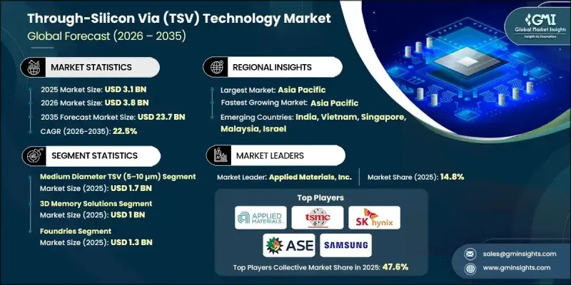
对紧凑、节能型半导体解决方案日益增长的需求正在重塑全球晶片设计策略。先进无线网路的广泛应用推动了边缘设备和行动平台性能要求的不断提高,从而需要更小的尺寸和更高的频宽效率。 TSV 技术实现了垂直集成,在外形规格尺寸的同时提升了电气性能。随着较小製程节点的经济和技术限制日益凸显,製造商正逐渐放弃传统的平面缩放方式。三维架构和基于晶片组的设计正成为提升性能的可持续途径。自 1990 年代末期以来,堆迭式记忆体和感测器架构的采用一直在稳步加速。到 21 世纪 20 年代初,大多数集成设备製造商已将支援 TSV 的三维设计纳入其长期性能规划。展望未来十年,垂直堆迭将成为处理器和加速器发展的关键驱动力。同时,区域化的半导体生产和自动化主导的製造正在重塑 TSV 供应链。与铜填充、晶圆减薄和平面化差异相关的初始製程限制推动了整个製造流程的持续改进。
| 市场覆盖范围 | |
|---|---|
| 开始年份 | 2025 |
| 预测年份 | 2026-2035 |
| 起始值 | 31亿美元 |
| 预测金额 | 237亿美元 |
| 复合年增长率 | 22.5% |
中等直径的硅通孔(TSV,5-10微米)占据最大市场份额,预计2025年市场规模将达到17亿美元。对小型化、热效率和可靠供电的需求不断增长,推动了先进3D封装解决方案的普及。该领域的製造商正致力于提高製造精度、热稳定性、能源效率和可扩展的成本结构,以支援半导体装置密度的不断提升。
预计到2025年,3D储存解决方案市场规模将达10亿美元。新一代高频宽记忆体的商业化正在加速采用TSV技术的堆迭式储存架构的普及。大规模运算环境的需求推动了对具有高速互连性能的垂直整合记忆体的需求,进一步凸显了基于TSV的设计在低延迟资料处理方面的重要性。
美国穿透硅通孔(TSV)技术市场预计到2025年将达到5.12亿美元,并在2026年至2035年间以22.3%的复合年增长率成长。联邦政府投入527亿美元支持国内製造业、外包半导体组装测试以及先进封装倡议。这项投资将促进TSV技术在记忆体、处理器和人工智慧加速器领域的应用,同时也有助于增强美国供应链的韧性。资料中心中晶片和高密度运算的日益普及进一步推动了市场需求,促使製造商将基础设施投资与国内代工厂和云端服务供应商对接。
目录
第一章调查方法和范围
第二章执行摘要
第三章业界考察
- 产业生态系分析
- 影响价值链的因素
- 利润率分析
- 中断
- 未来展望
- 製造商
- 经销商
- 影响因素
- 成长驱动因素
- 需要小型化的移动和 5G/Edge 设备
- 区域工厂和政府支持
- 人工智慧/高效能运算中的频宽和密度需求
- 异质整合(晶片组、2.5D/3D积体电路)
- 製造业生态系的成熟度与资本投资
- 产业潜在风险与挑战
- 製造成本、製程复杂性与产量比率损失
- 热机械可靠性(热膨胀係数 (CTE) 不匹配和应力)
- 机会
- 高效能运算 (HPC) 和人工智慧
- 3D堆迭式记忆体集成
- 成长驱动因素
- 成长潜力分析
- 监管环境
- 北美洲
- 欧洲
- 亚太地区
- 拉丁美洲
- 中东和非洲
- 波特分析
- PESTEL 分析
- 科技与创新趋势
- 当前技术趋势
- 新兴技术
- 新兴经营模式
- 合规要求
- 永续性措施
- 消费者心理分析
- 专利和智慧财产权分析
- 地缘政治和贸易趋势
第四章 竞争情势
- 介绍
- 公司市占率分析
- 按地区
- 北美洲
- 欧洲
- 亚太地区
- 拉丁美洲
- 中东和非洲
- 市场集中度分析
- 按地区
- 主要企业的竞争标竿分析
- 财务绩效比较
- 收入
- 利润率
- 研究与开发
- 产品系列比较
- 产品线丰富
- 科技
- 创新
- 按地区分類的企业发展比较
- 全球扩张分析
- 服务网路覆盖范围
- 按地区分類的市场渗透率
- 竞争定位矩阵
- 领导者
- 挑战者
- 追踪者
- 小众玩家
- 战略展望矩阵
- 财务绩效比较
- 主要发展(2022-2025)
- 併购
- 伙伴关係与合作
- 技术进步
- 业务拓展与投资策略
- 永续发展倡议
- 数位转型计划
- 新兴/Start-Ups竞赛的趋势
第五章 市场估算与预测:依TSV製程划分(2022-2035年)
- Via-first TSV
- VIA MiddleTSV
- 后导孔 TSV
第六章 市场估算与预测:依TSV直径划分(2022-2035年)
- 大直径TSV(超过10微米)
- 中等直径的TSV(5-10微米)
- 小直径TSV(小于5微米)
第七章 市场估计与预测:依应用领域划分(2022-2035 年)
- 3D 储存解决方案
- 高频宽体(HBM)
- 宽 I/O 内存
- 3D NAND快闪记忆体
- 处理器和计算设备
- CPU
- GPU
- 人工智慧加速器
- FPGA
- CMOS影像感测器
- MEMS元件
- 惯性感测器
- 压力感测器
- 麦克风
- 其他的
- 射频(RF)和通讯设备
- 其他的
第八章 依最终用途产业分類的市场估算与预测(2022-2035 年)
- 整合装置製造商(IDM)
- 铸造厂
- OSAT(半导体组装测试服务)
- 无晶圆厂半导体公司
- 其他的
第九章 各地区市场估算与预测(2022-2035 年)
- 北美洲
- 美国
- 加拿大
- 欧洲
- 英国
- 德国
- 法国
- 义大利
- 西班牙
- 俄罗斯
- 亚太地区
- 中国
- 印度
- 日本
- 韩国
- 澳洲
- 拉丁美洲
- 巴西
- 墨西哥
- 中东和非洲
- 南非
- 沙乌地阿拉伯
- 阿拉伯聯合大公国
第十章:公司简介
- 主要企业
- Applied Materials, Inc.
- Samsung
- Taiwan Semiconductor Manufacturing Company Limited
- SK Hynix
- Intel Corporation
- Lam Research
- Toshiba Corporation
- ASE Group
- 按地区分類的主要企业
- 北美洲
- Amkor Technology
- Atomica Corp
- 欧洲
- Okmetic Oyj
- Imec
- 亚太地区
- Japan Semiconductor Corporation
- Powertech Technology
- 北美洲
- 小众玩家/颠覆者
- Teledyne DALSA
- Nanosystems JP
The Global Through-Silicon Via (TSV) Technology Market was valued at USD 3.1 billion in 2025 and is estimated to grow at a CAGR of 22.5% to reach USD 23.7 billion by 2035.
Rising demand for compact, power-efficient semiconductor solutions continues to reshape chip design strategies worldwide. Increased deployment of advanced wireless networks places greater performance expectations on edge devices and mobile platforms, driving the need for smaller footprints and higher bandwidth efficiency. TSV technology enables vertical integration that reduces form factor size while improving electrical performance. Manufacturers increasingly shift away from conventional planar scaling as economic and technical limitations emerge at smaller nodes. Three-dimensional architectures and chiplet-based designs gain traction as viable pathways to sustain performance gains. Since the late 1990s, the adoption of stacked memory and sensor architectures steadily accelerated. By the early 2020s, most integrated device manufacturers incorporate TSV-enabled three-dimensional designs into long-term performance planning. Toward the next decade, vertical stacking becomes a primary driver of advancement for processors and accelerators. At the same time, regionalized semiconductor production and automation-driven manufacturing reshape TSV supply chains. Early process limitations related to copper filling, wafer thinning, and planarization variability drive continuous improvement efforts across fabrication workflows.
| Market Scope | |
|---|---|
| Start Year | 2025 |
| Forecast Year | 2026-2035 |
| Start Value | $3.1 Billion |
| Forecast Value | $23.7 Billion |
| CAGR | 22.5% |
The medium diameter TSVs, ranging from 5 to 10 micrometers, represent the largest segment and generated USD 1.7 billion in 2025. Growing requirements for miniaturization, thermal efficiency, and reliable power delivery encourage broader adoption of advanced three-dimensional packaging solutions. Manufacturers in this segment focus on achieving precision manufacturing, thermal stability, energy efficiency, and scalable cost structures to support rising volumes of high-density semiconductor devices.
The three-dimensional memory solutions segment generated USD 1 billion in 2025. Commercial availability of next-generation high-bandwidth memory accelerates the use of TSV-enabled stacked memory architectures. Demand from large-scale computing environments increases the need for vertically integrated memory with fast interconnect performance, reinforcing the importance of TSV-based designs for low-latency data processing.
U.S. Through-Silicon Via (TSV) Technology Market reached USD 512 million in 2025 and is projected to grow at a CAGR of 22.3% from 2026 to 2035. Federal funding of USD 52.7 billion supports domestic fabrication, outsourced semiconductor assembly and testing, and advanced packaging initiatives. This investment strengthens TSV adoption across memory, processors, and artificial intelligence accelerators while supporting national supply chain resilience. Expanding use of chiplets and high-density computing in data centers further drives demand, encouraging manufacturers to align infrastructure investments with domestic foundries and cloud service providers.
Key companies active in the Global Through-Silicon Via (TSV) Technology Market include Taiwan Semiconductor Manufacturing Company Limited, Intel Corporation, Applied Materials, Inc., Samsung, ASE Group, Lam Research, Amkor Technology, SK Hynix, Toshiba Corporation, Powertech Technology, Okmetic Oyj, Teledyne DALSA, Atomica Corp, Japan Semiconductor Corporation, Nanosystems JP, and imec. Companies operating in the Global Through-Silicon Via (TSV) Technology Market strengthen their competitive position through sustained investment in advanced packaging research, process automation, and yield optimization. Strategic collaboration across foundries, OSATs, and system designers supports faster adoption of three-dimensional integration. Many players focus on co-development frameworks to align TSV architectures with next-generation processors and memory platforms. Expanding localized manufacturing capacity improves supply chain security and reduces production risk. Firms also emphasize scalable process technologies that lower the cost per interconnect while improving reliability.
Table of Contents
Chapter 1 Methodology & Scope
- 1.1 Market scope and definition
- 1.2 Research design
- 1.2.1 Research approach
- 1.2.2 Data collection methods
- 1.3 Data mining sources
- 1.3.1 Global
- 1.3.2 Regional/Country
- 1.4 Base estimates and calculations
- 1.4.1 Base year calculation
- 1.4.2 Key trends for market estimation
- 1.5 Primary research and validation
- 1.5.1 Primary sources
- 1.6 Forecast model
- 1.7 Research assumptions and limitations
Chapter 2 Executive Summary
- 2.1 Industry 360° synopsis
- 2.2 Key market trends
- 2.2.1 TSV process trends
- 2.2.2 TSV diameter trends
- 2.2.3 Application trends
- 2.2.4 End-use industry trends
- 2.2.5 Regional trends
- 2.3 TAM Analysis, 2026-2035 (USD Billion)
- 2.4 CXO perspectives: Strategic imperatives
- 2.4.1 Executive decision points
- 2.4.2 Critical Success Factors
- 2.5 Future Outlook and Strategic Recommendations
Chapter 3 Industry Insights
- 3.1 Industry ecosystem analysis
- 3.1.1 Factor affecting the value chain
- 3.1.2 Profit margin analysis
- 3.1.3 Disruptions
- 3.1.4 Future outlook
- 3.1.5 Manufacturers
- 3.1.6 Distributors
- 3.2 Impact forces
- 3.2.1 Growth drivers
- 3.2.1.1 Mobile & 5G / edge devices needing miniaturization
- 3.2.1.2 Regional fabs and government support
- 3.2.1.3 AI / HPC demand for bandwidth & density
- 3.2.1.4 Heterogeneous integration (chiplets, 2.5D/3D ICs)
- 3.2.1.5 Manufacturing ecosystem maturation & equipment investment
- 3.2.2 Industry pitfalls & challenges
- 3.2.2.1 Manufacturing cost, process complexity & yield loss
- 3.2.2.2 Thermo-mechanical reliability (CTE mismatch & stress)
- 3.2.3 Opportunities
- 3.2.3.1 High-Performance Computing (HPC) & AI
- 3.2.3.2 3D Stacked Memory Integration
- 3.2.1 Growth drivers
- 3.3 Growth potential analysis
- 3.4 Regulatory landscape
- 3.4.1 North America
- 3.4.2 Europe
- 3.4.3 Asia Pacific
- 3.4.4 Latin America
- 3.4.5 Middle East & Africa
- 3.5 Porter's analysis
- 3.6 PESTEL analysis
- 3.7 Technology and Innovation landscape
- 3.7.1 Current technological trends
- 3.7.2 Emerging technologies
- 3.8 Emerging Business Models
- 3.9 Compliance Requirements
- 3.10 Sustainability Measures
- 3.11 Consumer Sentiment Analysis
- 3.12 Patent and IP analysis
- 3.13 Geopolitical and trade dynamics
Chapter 4 Competitive Landscape, 2025
- 4.1 Introduction
- 4.2 Company market share analysis
- 4.2.1 By region
- 4.2.1.1 North America
- 4.2.1.2 Europe
- 4.2.1.3 Asia Pacific
- 4.2.1.4 Latin America
- 4.2.1.5 Middle East & Africa
- 4.2.2 Market Concentration Analysis
- 4.2.1 By region
- 4.3 Competitive Benchmarking of key Players
- 4.3.1 Financial Performance Comparison
- 4.3.1.1 Revenue
- 4.3.1.2 Profit Margin
- 4.3.1.3 R&D
- 4.3.2 Product Portfolio Comparison
- 4.3.2.1 Product Range Breadth
- 4.3.2.2 Technology
- 4.3.2.3 Innovation
- 4.3.3 Geographic Presence Comparison
- 4.3.3.1 Global Footprint Analysis
- 4.3.3.2 Service Network Coverage
- 4.3.3.3 Market Penetration by Region
- 4.3.4 Competitive Positioning Matrix
- 4.3.4.1 Leaders
- 4.3.4.2 Challengers
- 4.3.4.3 Followers
- 4.3.4.4 Niche Players
- 4.3.5 Strategic outlook matrix
- 4.3.1 Financial Performance Comparison
- 4.4 Key developments, 2022-2025
- 4.4.1 Mergers and Acquisitions
- 4.4.2 Partnerships and Collaborations
- 4.4.3 Technological Advancements
- 4.4.4 Expansion and Investment Strategies
- 4.4.5 Sustainability Initiatives
- 4.4.6 Digital Transformation Initiatives
- 4.5 Emerging/ Startup Competitors Landscape
Chapter 5 Market Estimates & Forecast, By TSV Process Type, 2022-2035 (USD Billion)
- 5.1 Key trends
- 5.2 Via-First TSV
- 5.3 Via-Middle TSV
- 5.4 Via-Last TSV
Chapter 6 Market Estimates & Forecast, By TSV Diameter, 2022-2035 (USD Billion)
- 6.1 Key trends
- 6.2 Large diameter TSV (>10 µm)
- 6.3 Medium diameter TSV (5-10 µm)
- 6.4 Small diameter TSV (<5 µm)
Chapter 7 Market Estimates & Forecast, By Application, 2022-2035 (USD Billion)
- 7.1 Key trends
- 7.2 3D memory solutions
- 7.2.1 High bandwidth memory (HBM)
- 7.2.2 Wide I/O memory
- 7.2.3 3D NAND flash memory
- 7.3 Processors & compute devices
- 7.3.1 CPUs
- 7.3.2 GPUs
- 7.3.3 AI Accelerators
- 7.3.4 FPGAs
- 7.4 CMOS image sensors
- 7.5 MEMS devices
- 7.5.1 Inertial sensors
- 7.5.2 Pressure sensors
- 7.5.3 Microphones
- 7.5.4 Others
- 7.6 RF & communication devices
- 7.7 Others
Chapter 8 Market Estimates & Forecast, By End Use Industry, 2022-2035 (USD Billion)
- 8.1 Key trends
- 8.2 Integrated device manufacturers (IDMs)
- 8.3 Foundries
- 8.4 OSATs (Outsourced semiconductor assembly & test)
- 8.5 Fabless semiconductor companies
- 8.6 Others
Chapter 9 Market Estimates & Forecast, By Region, 2022-2035 (USD Billion)
- 9.1 Key trends
- 9.2 North America
- 9.2.1 U.S.
- 9.2.2 Canada
- 9.3 Europe
- 9.3.1 UK
- 9.3.2 Germany
- 9.3.3 France
- 9.3.4 Italy
- 9.3.5 Spain
- 9.3.6 Russia
- 9.4 Asia Pacific
- 9.4.1 China
- 9.4.2 India
- 9.4.3 Japan
- 9.4.4 South Korea
- 9.4.5 Australia
- 9.5 Latin America
- 9.5.1 Brazil
- 9.5.2 Mexico
- 9.6 MEA
- 9.6.1 South Africa
- 9.6.2 Saudi Arabia
- 9.6.3 UAE
Chapter 10 Company Profiles
- 10.1 Global Key Players
- 10.1.1 Applied Materials, Inc.
- 10.1.2 Samsung
- 10.1.3 Taiwan Semiconductor Manufacturing Company Limited
- 10.1.4 SK Hynix
- 10.1.5 Intel Corporation
- 10.1.6 Lam Research
- 10.1.7 Toshiba Corporation
- 10.1.8 ASE Group
- 10.2 Regional Key Players
- 10.2.1 North America
- 10.2.1.1 Amkor Technology
- 10.2.1.2 Atomica Corp
- 10.2.2 Europe
- 10.2.2.1 Okmetic Oyj
- 10.2.2.2 Imec
- 10.2.3 Asia Pacific
- 10.2.4 Japan Semiconductor Corporation
- 10.2.5 Powertech Technology
- 10.2.1 North America
- 10.3 Niche Players/Disruptors
- 10.3.1 Teledyne DALSA
- 10.3.2 Nanosystems JP
 全球防静电载带捲市场(按载带类型、材料、胶带材料成分、胶带层数和最终用途产业划分)预测(2026-2032年)导线架固定胶带市场(按黏合剂类型、背衬材料、胶带宽度、胶带厚度、应用、最终用途行业和销售管道),全球预测,2026-2032年
 MEMS封装焊料市场规模、份额和成长分析:按焊料类型、产品形式、应用、封装类型、最终用户和地区划分 - 2026-2033年产业预测
 先进半导体封装市场分析及预测(至2035年):依类型、产品类型、服务、技术、应用、材料类型、装置、製程、最终用户及功能划分半导体原型製作及封装市场分析及预测(至2035年):依类型、产品类型、服务、技术、应用、材料类型、组件、製程、最终用户、设备划分半导体封装市场分析及预测(至2035年):依类型、产品类型、技术、应用、材料类型、装置、製程、最终用户、功能、设备划分
 高端半导体封装:市场占有率分析、产业趋势与统计、成长预测(2026-2031)
 3-D TSV:关键问题洞察与市场分析
 高密度封装(MCM、MCP、SIP、3D-TSV):市场分析与技术趋势
 2026年全球四方扁平包装市场报告