


 |
市场调查报告书
商品编码
1550010
化学机械抛光 (CMP)垫片:市场占有率分析、行业趋势、成长预测(2024-2029 年)Chemical Mechanical Polishing (CMP) Pad - Market Share Analysis, Industry Trends & Statistics, Growth Forecasts (2024 - 2029) |
||||||
※ 本网页内容可能与最新版本有所差异。详细情况请与我们联繫。
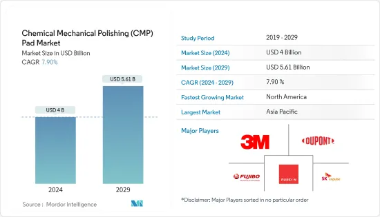
化学机械抛光(CMP)垫片市场规模预计到 2024 年为 40 亿美元,预计到 2029 年将达到 56.1 亿美元,预测期内(2024-2029 年)复合年增长率为 7.90%。
主要亮点
- 化学机械抛光是半导体晶圆製造过程中的关键步骤。在此过程中,晶圆的顶面被抛光以形成完美平坦的表面。这对于将化学浆料与机械运动相结合以创造更坚固耐用的半导体材料至关重要。
- 随着电子设备性能标准的提高,半导体和电子设备需要更小、更耐用。因此,对 CMP 等先进製造材料和技术的需求不断增加。对电子产品不断增长的需求正在推动电子封装行业的发展,客户期望新电子设备具有增强的功能。
- 半导体产业是化学机械抛光垫片的重要消费者,特别是在半导体製造过程中的晶圆抛光过程中。在汽车电子、智慧型手机、物联网设备和人工智慧 (AI) 技术等应用的推动下,对半导体的需求不断增长,从而推动了对化学机械抛光垫片的需求。此外,半导体製造技术的不断进步(例如小型化)正在推动对更精确、更有效率的 CMP垫片的需求。
- 3DE IC、穿透硅通孔(TSV) 和扇出晶圆级封装 (FOWLP) 等封装技术的日益普及需要先进的 CMP 抛光和表面处理解决方案。化学机械抛光 (CMP)垫片对于实现这些先进封装製程所需的抛光、表面粗糙度和缺陷水平至关重要。
- 儘管化学机械抛光 (CMP)垫片材料和製造过程取得了进步,但某些技术限制仍然存在。这些限制包括实现超光滑表面、抑製表面下损伤、最小化边缘效应以及解决垫片磨损和浆料消费量问题。可能需要进一步的研究和开发来克服这些限制,这是阻碍市场成长的一个因素。此外,CMP垫片製造商可能面临与供应链中断相关的风险,影响其满足需求的能力。
- 技术进步、材料科学创新和製程工程发展等宏观经济因素正在为 CMP垫片製造商带来挑战和机会。解决与 CMP 製程控制、减少缺陷、材料相容性和表面品质改进相关的技术问题正在推动 CMP垫片市场的研发投资和产品创新。相反,CMP垫片材料、配方和製造技术的突破可以为创新供应商创造竞争优势和市场机会。
化学机械抛光(CMP)垫片市场趋势
300mm晶圆尺寸将大幅成长
- 在半导体产业,由于先进的製造工艺,晶圆尺寸几乎已经标准化在300mm左右。这种标准化简化了供应链物流,并促进了半导体製造商、设备供应商和材料供应商之间的协作。因此,化学机械抛光 (CMP)垫片製造商正在优先开发和生产专为 300 mm 晶圆加工设计的 CMP垫片,以满足产业需求。
- 全球300毫米晶圆厂产能扩张步伐正在放缓。然而,该行业仍专注于提高产能,以满足强劲而稳定的半导体需求。例如,印度计划于 2024 年 3 月开始生产半导体製造设备,应用材料公司率先在班加罗尔建立了验证中心。我们在300mm晶圆加工方面也取得了进展,并在建立工程中心的同时致力于建立生态系统。这些技术创新正在推动研究目标市场的成长。
- 2023 年 11 月,德克萨斯(TI) 在华盛顿州李海市推出了名为 LFAB2 的新型 300 毫米半导体晶圆製造厂。 LFAB2 的建设将连接到该公司在该地点现有的 300 毫米晶圆厂。一旦完成,LFAB2 将使 TI 犹他工厂能够每天满载生产数千万个嵌入式和类比处理晶片。 LFAB2 的目标是完全依靠可再生电力运行,在李海安装 300mm 先进设备和製程将有助于最大限度地减少废弃物、水和能源的使用。
- 晶圆尺寸向 300mm 的转变通常与采用先进的半导体製造技术和缩小製程节点(7nm 和 5nm)有关。这些先进的节点技术需要更严格的製程控制和增强的抛光,以满足严格的性能和可靠性要求。
- 化学机械抛光 (CMP)垫片的需求量很大,因为它们在实现先进节点製造所需的奈米级平坦度方面发挥关键作用。
亚太地区占主要市场占有率
- 亚太地区是世界半导体製造中心,中国、台湾、韩国、日本等国家在半导体製造领域扮演重要角色。该地区半导体製造业的成长推动了对晶圆抛光製程中使用的化学机械抛光 (CMP)垫片的强劲需求。
- 亚太地区处于技术进步的前沿,包括先进封装技术、高效能运算和人工智慧(AI)的发展。这些进步需要精确、高效的 CMP 工艺,从而推动了对 CMP垫片的需求。
- 该地区继续投资新的半导体製造设施(晶圆厂)并扩大现有设施。工厂产能的增加和先进製造设备的引进正在推动CMP垫片消费量的增加。例如,2024年3月,塔塔电子私人有限公司(TEPL)与台湾力晶半导体製造公司(PSMC)合作,在古吉拉突邦Dholera设立半导体工厂。该计划投资额为9.1兆印度卢比(1,097.1亿美元)。 PSMC 目前在台湾经营六家半导体代工厂。
- 新晶圆厂的产能将达到每月 50,000 片晶圆。 PSMC将专注于使用28奈米技术生产高性能运算和电源管理晶片,用于电动车、电讯、国防、汽车、消费性电子、显示器和电力电子等各个产业。
- 在可支配收入增加、都市化和技术采用的推动下,亚太地区消费性电子市场正在经历显着扩张。对智慧型手机、笔记型电脑和电子设备的需求正在增加对半导体元件和 CMP垫片的需求。
- 此外,印度、越南和印尼等亚太地区的新兴经济体在各领域也越来越多地采用半导体技术。这些国家的工业化和数数位化正在取得进展,半导体製造对 CMP垫片的需求预计将大幅成长。
- 智慧城市、5G网路和物联网等正在进行的基础设施开发计划正在推动对半导体晶片和电子元件的需求。化学机械抛光 (CMP)垫片在生产这些基础设施计划所需的先进半导体元件方面发挥关键作用。
- 此外,亚太地区的政府和产业正在投资半导体研发以促进创新。旨在开发下一代材料、设备和製程的研究倡议正在促进对 CMP垫片的需求。
化学机械抛光 (CMP)垫片产业概览
化学机械抛光(CMP)垫片市场竞争非常激烈。公司种类繁多,从大到小,所以非常集中。所有主要公司都占有重要的市场占有率,并致力于扩大其全球消费群。该市场的重要参与者包括 3M、杜邦、富士纺控股、Purion 和 SK Anpulse。为了在预测期内获得竞争优势,多家公司正在透过结盟、合作、收购和推出创新新产品来扩大市场占有率。
- 2024年4月,决定SK海力士继续在韩国的投资计画。该公司正准备投资120兆日圆(7,400亿美元)在龙仁半导体丛集建设生产设施。第一家工厂预计将于 2025 年 3 月开始建设,并于 2027 年初竣工。还将建造一座小型晶圆厂,使用 300 毫米晶圆加工设备来测试半导体材料、组件和设备。
- 2023年9月,SK Empulse出售了半导体基础材料业务,湿化学业务被当地半导体/显示材料公司Yaker Technology收购,清洗业务被投资公司Sunyang Shinjin收购。今年早些时候,SKC将其半导体材料和零件业务整合到SK Empulse,扩大了其在半导体前端工艺的高付加材料业务中的影响力,例如化学机械抛光(CMP)垫片和空白掩模。
其他好处:
- Excel 格式的市场预测 (ME) 表
- 3 个月分析师支持
目录
第一章简介
- 研究假设和市场定义
- 调查范围
第二章调查方法
第三章执行摘要
第四章市场洞察
- 市场概况
- 产业吸引力-波特五力分析
- 新进入者的威胁
- 买家/消费者的议价能力
- 供应商的议价能力
- 替代品的威胁
- 竞争公司之间的敌对关係
- 技术简介
- COVID-19 和其他宏观经济因素对市场的影响
第五章市场动态
- 市场驱动因素
- 对复杂、高性能晶片/先进技术的需求不断增长
- 小节点与新架构简介
- 市场限制因素
- 半导体产业的週期性和动态性
第六章 市场细分
- 按晶圆尺寸
- 300 mm
- 200 mm
- 其他晶圆尺寸
- 按地区
- 北美洲
- 欧洲
- 中国
- 韩国
- 日本
- 台湾
第七章 竞争格局
- 公司简介
- 3M Co.
- DuPont de Nemours Inc.
- Fujibo Holdings Inc.
- Pureon
- SK enpulse
- Thomas West Inc.
- Hubei DingLong
- Cabot Corporation
- Entegris
- Beijing Grish Hitech Co. Ltd
第八章投资分析
第9章市场的未来
The Chemical Mechanical Polishing Pad Market size is estimated at USD 4 billion in 2024, and is expected to reach USD 5.61 billion by 2029, growing at a CAGR of 7.90% during the forecast period (2024-2029).
Key Highlights
- Chemical mechanical polishing is a crucial step in the semiconductor wafer manufacturing process. During this process, the top surface of the wafer is polished to create a completely flat surface, which is essential for building more robust and durable semiconductor materials using a combination of chemical slurry and mechanical movements.
- The rising performance standards of electronic devices are leading to a need for smaller and more durable semiconductors and electronic devices. This, in turn, increases the requirement for advanced fabrication materials and techniques such as CMP. The growing demand for electronic products drives the electronic packaging industry, with customers expecting enhanced features in new electronic devices.
- The semiconductor industry is a significant consumer of chemical mechanical polishing pads, particularly for wafer polishing processes during semiconductor manufacturing. The increasing demand for semiconductors driven by applications such as automotive electronics, smartphones, IoT devices, and AI (artificial intelligence) technologies fuels the demand for chemical mechanical polishing pads. Moreover, the continuous technological advancements in semiconductor fabrication technologies, including the development of smaller feature sizes, drive the need for more precise and efficient CMP pads.
- The rising adoption of packaging technologies such as 3DE ICs, through-silicon vias(TSVs), and fan-out wafer-level packaging (FOWLP) necessitates advanced CMP polishing and surface preparation solutions. Chemical mechanical polishing (CMP) pads are crucial in achieving the required polishing, surface roughness, and defectivity levels of these advanced packaging processes.
- Despite the advancements in chemical mechanical polishing (CMP) pad materials and manufacturing processes, certain technological limitations persist. These limitations include achieving ultra-smooth surfaces, controlling sub-surface damage, minimizing edge effects, and addressing pad wear and slurry consumption issues. Overcoming these limitations may require further research and development efforts, thus hindering the market's growth. Moreover, CMP pad manufacturers may face risks associated with supply chain disruptions, impacting the ability to meet demand.
- Macroeconomic factors such as technological advancements, material science innovations, and process engineering developments are presenting challenges and opportunities for CMP pad manufacturers. Addressing technical difficulties related to CMP process control, defect reduction, material compatibility, and surface quality improvement drives R&D investments and product innovation in the CMP pads market. Conversely, breakthroughs in CMP pad materials, formulations, or manufacturing techniques can create competitive advantages and market opportunities for innovative suppliers.
Chemical Mechanical Polishing (CMP) Pad Market Trends
300 mm Wafer Size to Witness a Significant Growth
- The semiconductor industry has largely standardized around 300 mm wafer size for advanced manufacturing processes. This standardization simplifies supply chain logistics and facilitates collaboration among semiconductor manufacturers, equipment suppliers, and materials providers. As a result, chemical mechanical polishing (CMP) pad manufacturers prioritize developing and producing CMP pads designed for 300 mm wafer processing to meet the industry demand.
- The rate of global 300 mm fab capacity expansion is slowing down. However, the industry is still dedicated to increasing capacity to keep up with the firm and consistent semiconductor demand. For instance, in March 2024, India planned to produce equipment for semiconductor manufacturing, with Applied Materials taking the lead by establishing a validation center in Bengaluru. The country is also advancing in 300 mm wafer processing and is focusing on creating a supportive ecosystem while establishing an engineering center. These innovations are driving the growth of the market studied.
- In November 2023, Texas Instruments launched a new 300 mm semiconductor wafer fabrication plant called LFAB2 in Lehi, Utah. The construction of LFAB2 will be connected to the company's existing 300 mm wafer fab in the exact location. Once LFAB2 is finished, both of TI's Utah fabs will be capable of producing tens of millions of embedded and analog processing chips daily at maximum capacity. LFAB2 aims to operate solely on renewable electricity, and the implementation of advanced 300 mm equipment and processes in Lehi will help minimize waste, water, and energy usage.
- The shift to 300 mm wafer size is often associated with adopting advanced semiconductor manufacturing technologies and smaller process nodes (7 nm and 5 nm). These advanced node technologies require tighter process control and enhanced polishing to meet stringent performance and reliability requirements.
- Chemical mechanical polishing (CMP) pads are in high demand because they play a crucial role in achieving the nanoscale-level planarity required for advanced node fabrication.
Asia-Pacific to Hold Significant Market Share
- Asia-Pacific is a global semiconductor manufacturing hub, with countries like China, Taiwan, South Korea, and Japan playing significant roles in semiconductor fabrication. The region's growth in semiconductor manufacturing drives the substantial demand for chemical mechanical polishing (CMP) pads used in wafer polishing processes.
- Asia-Pacific is at the forefront of technological advancements, including developing advanced packaging technologies, high-performance computing, and AI (artificial intelligence). These advancements require precise and efficient CMP processes, boosting the demand for CMP pads.
- The region continues to witness investments in new semiconductor fabrication facilities (fabs) and the expansion of existing ones. Increasing fab capacity and installing advanced manufacturing equipment contribute to the higher consumption of CMP pads. For instance, in March 2024, Tata Electronics Private Limited (TEPL) partnered with Taiwan's Powerchip Semiconductor Manufacturing Corp. (PSMC) to set up a semiconductor fab in Dholera, Gujarat. The investment for this project is INR 9,100 billion (USD 109.71 billion). PSMC currently operates six semiconductor foundries in Taiwan.
- The capacity of the new fabs will be 50,000 wafer starts per month. PSMC will focus on producing high-performance compute chips using 28 nm technology and power management chips for various industries such as electric vehicles, telecom, defense, automotive, consumer electronics, display, and power electronics.
- Asia-Pacific is home to a large and expanding consumer electronics market driven by rising disposable incomes, urbanization, and technological proliferation. The demand for smartphones, laptops, and electronic devices fuels the need for semiconductor components and CMP pads.
- Moreover, emerging economies in Asia-Pacific, such as India, Vietnam, and Indonesia, are witnessing increasing adoption of semiconductor technologies across various sectors. As these economies continue to industrialize and digitize, the demand for CMP pads for semiconductor manufacturing is expected to grow significantly.
- Ongoing infrastructure development projects, such as smart cities, 5G networks, and the IoT, drive demand for semiconductor chips and electronic components. The chemical mechanical polishing (CMP) pads play a significant role in enabling the production of advanced semiconductor devices required for these infrastructure projects.
- In addition, governments and industries in Asia-Pacific are investing in semiconductor R&D to foster innovation. Research initiatives aimed at developing next-generation materials, devices, and processes contribute to the demand for CMP pads.
Chemical Mechanical Polishing (CMP) Pad Industry Overview
The chemical mechanical polishing (CMP) pads market is very competitive. It is highly concentrated due to various large and small players. All the major players account for a significant market share and focus on expanding the global consumer base. Some significant players in the market are 3M Co, DuPont de Nemours Inc., Fujibo Holdings Inc., Pureon, and SK enpulse. Several companies are increasing their market share by forming collaborations, partnerships, and acquisitions and introducing new and innovative products to earn a competitive edge during the forecast period.
- In April 2024, SK Hynix was set to continue with its scheduled investments in Korea. The company is getting the Yongin Semiconductor Cluster site ready to construct production facilities, with an investment of JPY 120 trillion (USD 0.74 trillion). The first fab was expected to start construction in March 2025 and be completed by early 2027. A mini fab will also be constructed to test semiconductor materials, components, and equipment using 300 mm wafer processing equipment.
- In September 2023, SK enpulse divested its semiconductor basic materials business, with the wet chemical business purchased by the local semiconductor/display materials company Yaker Technology and the cleaning business acquired by the investment company Sunyang Shinjin. Earlier this year, SKC consolidated its semiconductor materials/parts businesses into SK enpulse to enhance its presence in high-value-added materials business areas for semiconductor front-end processes, such as chemical mechanical polishing (CMP) pads and blank masks.
Additional Benefits:
- The market estimate (ME) sheet in Excel format
- 3 months of analyst support
TABLE OF CONTENTS
1 INTRODUCTION
- 1.1 Study Assumptions and Market Definition
- 1.2 Scope of the Study
2 RESEARCH METHODOLOGY
3 EXECUTIVE SUMMARY
4 MARKET INSIGHTS
- 4.1 Market Overview
- 4.2 Industry Attractiveness - Porter's Five Forces Analysis
- 4.2.1 Threat of New Entrants
- 4.2.2 Bargaining Power of Buyers/Consumers
- 4.2.3 Bargaining Power of Suppliers
- 4.2.4 Threat of Substitute Products
- 4.2.5 Intensity of Competitive Rivalry
- 4.3 Technology Snapshot
- 4.4 Impact of COVID-19 Aftereffects and Other Macroeconomic Factors on the Market
5 MARKET DYNAMICS
- 5.1 Market Drivers
- 5.1.1 Increasing Need for Complex and High-Performance Chips/Advanced Technologies
- 5.1.2 Introduction of Smaller Nodes and New Architectures
- 5.2 Market Restraints
- 5.2.1 Cyclic and Dynamic Nature of the Semiconductor Industry
6 MARKET SEGMENTATION
- 6.1 By Wafer Size
- 6.1.1 300 mm
- 6.1.2 200 mm
- 6.1.3 Other Wafer Sizes
- 6.2 By Geography
- 6.2.1 North America
- 6.2.2 Europe
- 6.2.3 China
- 6.2.4 South Korea
- 6.2.5 Japan
- 6.2.6 Taiwan
7 COMPETITIVE LANDSCAPE
- 7.1 Company Profiles
- 7.1.1 3M Co.
- 7.1.2 DuPont de Nemours Inc.
- 7.1.3 Fujibo Holdings Inc.
- 7.1.4 Pureon
- 7.1.5 SK enpulse
- 7.1.6 Thomas West Inc.
- 7.1.7 Hubei DingLong
- 7.1.8 Cabot Corporation
- 7.1.9 Entegris
- 7.1.10 Beijing Grish Hitech Co. Ltd
8 INVESTMENT ANALYSIS
9 FUTURE OF THE MARKET
 CMP设备及耗材:市场分析与预测
 2026年全球化学机械抛光(CMP)软垫市场报告
 12吋CMP设备市场:按技术、浆料类型、垫片材质、应用和最终用途产业划分-2026-2032年全球预测半导体CMP抛光浆料市场按浆料类型、磨料类型、pH值、粒径、最终用户和分销管道划分-全球预测(2026-2032年)
 化学机械抛光市场:依抛光机类型、晶圆尺寸、製程类型、抛光液类型、应用、最终用户、国家及地区划分-产业分析、市场规模、市场份额及2024-2032年预测
 化学机械抛光市场-2025-2030年预测
 化学机械抛光(CMP)-全球市场份额和排名、总收入和需求预测(2025-2031年)CMP保持环 - 全球市场份额和排名、总收入和需求预测(2025-2031年)化学机械平坦化垫片市场(依产品类型、材质、晶圆尺寸、最终用途和孔径尺寸划分)-全球预测,2025-2032年按晶圆尺寸、应用、磨床类型、製程类型、最终用户和抛光液类型分類的化学机械抛光市场-全球预测,2025-2032年