


 |
市场调查报告书
商品编码
1907242
奈米感测器:市场份额分析、产业趋势与统计、成长预测(2026-2031)Nanosensors - Market Share Analysis, Industry Trends & Statistics, Growth Forecasts (2026 - 2031) |
||||||
※ 本网页内容可能与最新版本有所差异。详细情况请与我们联繫。
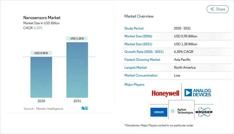
预计到 2025 年,奈米感测器市场价值将达到 8.9 亿美元,到 2026 年将成长至 9.5 亿美元,到 2031 年将成长至 12.8 亿美元,在预测期(2026-2031 年)内复合年增长率为 6.30%。
这一成长主要由三大支柱驱动:电子和医疗保健领域的微型化压力、量子点製造成本的快速下降以及预测性维护物联网系统的日益普及。政府的奈米技术计画、照护现场技术的应用以及国防领域对微量爆炸物检测的需求,持续扩大奈米感测器的潜在市场。随着大型半导体公司透过垂直整合来确保单壁奈米碳管的供应,竞争日益激烈,而一些专注于超选择性生化感测的利基开发商则致力于此。同时,监管机构正在製定奈米毒理学指南,一旦最终定稿,预计将加快产品核可。
全球奈米感测器市场趋势与洞察
电子设备的微型化及其在穿戴式装置中的集成
消费品和医疗设备製造商正在将尺寸小于100奈米的感测元件应用于产品中,这些元件能够在不增加设备体积的情况下追踪生物标记。苹果公司最新健康手錶整合了奈米感测器阵列,可连续监测血糖值和血氧饱和度,展现了商业性可行性,预计到2027年将带来2亿美元的潜在额外收入。三星的专利申请暗示了智慧型手机中即时过敏原检测技术的潜力,而航太零件也在利用奈米感测器测量密闭环境中的应力。美国食品药物管理局(FDA)对穿戴式医疗设备的快速审批流程缩短了产品推出週期,使创新者能够获得先发优势。
政府资助的奈米技术调查计画
公共支出支撑着长期需求。美国国家奈米技术倡议已为2024年累计18亿美元,其中约四分之一用于感测研究。中国的「十四五」规划和欧盟的「地平线欧洲」计画也投入了类似的资源用于量子点和奈米碳管设施建设,从而创造了对奈米感测器基板的强劲需求。国防机构已将这项技术视为战略性技术,即使在景气衰退时期也保障了其预算,并确保了采购合约的稳定供应。
复杂奈米製造扩充性的瓶颈
50奈米以下的微影製程需要极紫外线曝光设备,每台设备造价高达2亿美元,不仅令资本预算捉襟见肘,也限制了全球产能。产量比率低于60%,仅为典型半导体生产线良率的三分之一,导致单位成本高。台积电公开报告称,缺陷密度挑战导致生产成本比预期高出三倍。这些限制因素促使企业采用混合架构,削弱了全奈米级解决方案的性能优势。
细分市场分析
到2025年,化学奈米感测器将占据奈米感测器市场32.95%的主导份额,主要得益于医疗诊断和环境检测领域需求的成长。物理奈米感测器则因航太对高解析度压力和应变测量的需求而成为该领域成长最快的产品,年复合成长率(CAGR)达到7.08%。生物奈米感测器利用单分子检测技术进行药物监测,并在精准医疗领域占有一席之地。混合型奈米感测器将化学选择性与生物特异性相结合,例如雅培公司用于同时筛检多种生物标记的原型产品。监管机构对分析化学的日益深入理解正在推动化学奈米感测器核准,而机械工程领域的标准化则加速了物理感测器的应用。
同时,先进的表面功能化方法正在模糊类别界限,并推动跨学科应用。物理感测器受益于成熟的微机电系统(MEMS)工艺,降低了单位成本,吸引了汽车原始设备製造商(OEM)的注意。化学装置在水质监测领域持续获得应用,因为分子识别在水质监测中至关重要。生物奈米感测器则继续瞄准重症监护环境,这使其较高的价格也显得合理。
区域分析
到2025年,北美将占据奈米感测器市场30.95%的收入份额,这主要得益于国防合约、FDA核准的医疗设备以及蓬勃发展的创业融资生态系统。光是美国在2024年就为奈米感测器的研发拨款3.4亿美元。加拿大的量子点工厂和墨西哥经济高效的电子组装完善了该地区的供应链。监管部门的快速审批程序促进了市场准入,但严格的环境法规也带来了高昂的合规成本。
预计到2031年,亚太地区将以7.86%的复合年增长率成长,缩小与北美地区的差距。中国23亿美元的感测器计画、日本的「社会5.0」智慧城市计画以及韩国的K-Semiconductor Belt计画都在推动国内製造业的发展。低廉的营运成本吸引了全球製造业外包。新加坡和台湾地区供应高精准组件,而印度则在售后服务和校准领域崭露头角。
欧洲汽车和工业领域对奈米感测器的需求仍然强劲,其中德国在汽车排放气体检测领域主导。 REACH法规将延长认证週期,但精通合规的供应商将从中受益。法国和英国正在投资研发资金,用于国防相关的奈米感测器计画。中东和非洲地区正在油田监测领域推广应用奈米感测器,其耐用性在该领域具有很高的价值。南美洲则相对落后,目前仅限于一些专门的采矿和环境修復试点计画。
其他福利:
- Excel格式的市场预测(ME)表
- 3个月的分析师支持
目录
第一章 引言
- 研究假设和市场定义
- 调查范围
第二章调查方法
第三章执行摘要
第四章 市场情势
- 市场概览
- 市场驱动因素
- 电子设备小型化和可穿戴设备的集成
- 政府资助的奈米技术调查计画
- 照护现场的快速扩张
- 工业预测性维护物联网应用激增
- 国防部门对微量爆炸物和核子生化探测的需求
- 改善量子点成本曲线
- 市场限制
- 复杂奈米製造可扩展性的瓶颈
- 奈米毒理学标准监管方面的延误
- 高湿度场环境中的讯号漂移
- 集中高纯度单壁奈米碳管(SWCNTs)的供应链
- 供应链分析
- 监管环境
- 技术展望
- 宏观经济因素如何影响市场
- 波特五力分析
- 供应商的议价能力
- 消费者议价能力
- 新进入者的威胁
- 竞争对手之间的竞争
- 替代品的威胁
第五章 市场规模与成长预测
- 按类型
- 生物奈米感测器市场
- 化学奈米感测器市场
- 物理奈米感测器市场
- 透过使用
- 卫生保健
- 家用电子电器
- 航太/国防
- 汽车和工业
- 发电
- 其他终端用户产业
- 透过技术
- 电化学
- 光学
- 电磁学
- 压电
- 奈米力学
- 按地区
- 北美洲
- 美国
- 加拿大
- 墨西哥
- 南美洲
- 巴西
- 阿根廷
- 其他南美洲
- 欧洲
- 德国
- 英国
- 法国
- 义大利
- 西班牙
- 俄罗斯
- 其他欧洲地区
- 亚太地区
- 中国
- 日本
- 印度
- 韩国
- 东南亚
- 亚太其他地区
- 中东和非洲
- 中东
- 沙乌地阿拉伯
- 阿拉伯聯合大公国
- 其他中东地区
- 非洲
- 南非
- 埃及
- 其他非洲地区
- 中东
- 北美洲
第六章 竞争情势
- 市场集中度
- 策略趋势
- 市占率分析
- 公司简介
- Agilent Technologies Inc.
- Analog Devices Inc.
- OMRON Corporation
- Honeywell International Inc.
- Bruker Corporation
- Texas Instruments Inc.
- Lockheed Martin Corporation
- STMicroelectronics NV
- Robert Bosch GmbH
- Samsung Electronics Co. Ltd.
- Medtronic plc
- Universal Biosensors Inc.
- Hoffmann-La Roche Ltd.
- Nanowear Inc.
- AerBetic LLC
- Applied Nanodetectors Ltd.
- BreathDX Ltd.
- Inanon Bio Inc.
- LamdaGen Corporation
- Vista Therapeutics Inc.
- GBS Inc.
- Applied Nanotech Inc.(PEN Inc.)
- Oxonica Limited
- Beijing ALT Technology Co.
- NanoWorld AG
- Sensonor AS
- Synkera Technologies Inc.
第七章 市场机会与未来展望
The nanosensors market was valued at USD 0.89 billion in 2025 and estimated to grow from USD 0.95 billion in 2026 to reach USD 1.28 billion by 2031, at a CAGR of 6.30% during the forecast period (2026-2031).
This growth rests on three pillars: miniaturization pressures across electronics and healthcare, steep cost declines in quantum dot fabrication, and the widening adoption of predictive maintenance IoT systems. Government nanotechnology programs, point-of-care diagnostic rollouts, and defense demand for trace-explosive detection continue to broaden the addressable nanosensors market. Competitive intensity is rising as semiconductor leaders integrate vertically to secure a single-wall carbon nanotube supply, while niche developers focus on ultra-selective biochemical sensing. Simultaneously, regulators are drafting nano-toxicology guidelines that could accelerate product clearances once finalized.
Global Nanosensors Market Trends and Insights
Miniaturization of Electronics and Wearables Integration
Consumer and medical device makers are embedding sub-100 nm sensing elements that track biomarkers without enlarging device form factors. Apple's latest health watch integrates nanosensor arrays for continuous glucose and oxygen-saturation monitoring, illustrating commercial readiness and spurring a USD 200 million incremental addressable revenue by 2027. Samsung patent filings point to real-time allergen detection in smartphones, while aerospace components adopt nanosensors to measure strain in space-constrained environments. Faster FDA reviews for wearable medical devices shorten launch cycles, allowing innovators to capture early-mover advantages.
Government-Funded Nanotech Research Programs
Public spending anchors long-range demand. The U.S. National Nanotechnology Initiative earmarked USD 1.8 billion in 2024, with nearly one-quarter of the funding allocated to sensing research. China's 14th Five-Year Plan and the EU's Horizon Europe pour matching resources into quantum-dot and carbon-nanotube facilities, creating reliable demand for nanosensor substrates. Defense agencies treat the technology as strategic, insulating budgets even in downturns and ensuring a steady pipeline of procurement contracts.
Complex Nanofabrication Scalability Bottlenecks
Sub-50 nm lithography demands extreme-ultraviolet tools that cost USD 200 million each, pressing capital budgets and capping global output capacity. Yield rates remain below 60%, which is three times lower than the standard for semiconductor lines, thereby inflating unit economics. TSMC's public disclosures reveal defect-density hurdles that triple production costs versus projected metrics. These constraints force blended architectures that dilute the performance edge of fully nanoscale solutions.
Other drivers and restraints analyzed in the detailed report include:
- Rapid Expansion of Point-of-Care Diagnostics
- Surge in Industrial Predictive-Maintenance IoT Deployments
- Regulatory Lag on Nano-Toxicology Standards
For complete list of drivers and restraints, kindly check the Table Of Contents.
Segment Analysis
Chemical nanosensors held a dominant 32.95% share of the nanosensors market in 2025, driven by strong uptake in medical diagnostics and environmental testing. Physical variants registered a 7.08% CAGR, the fastest in class, fueled by aerospace demand for high-resolution pressure and strain measurement. Biological nanosensors occupy a niche in precision therapeutics, leveraging single-molecule detection for the monitoring of drugs. Hybrid devices now merge chemical selectivity with biological specificity, as evidenced by Abbott prototypes that simultaneously screen multiple biomarkers. Regulatory familiarity with analytical chemistry provides chemical nanosensors with a smoother path to approval, while mechanical engineering standards expedite the deployment of physical sensors.
In parallel, advanced surface-functionalization methods blur category lines, enabling cross-disciplinary applications. Physical sensors benefit from maturing MEMS processes that cut per-unit costs, drawing interest from automotive OEMs. Chemical devices remain favored in water-quality monitoring where molecular discrimination is crucial. Biological nanosensors continue to target intensive-care environments that justify premium pricing.
The Nanosensors Market Report is Segmented by Type (Biological Nanosensors, Chemical Nanosensors, and More), End-Use Verticals (Healthcare, Consumer Electronics, Aerospace and Defense, and More), Technology (Electrochemical, Optical, Electromagnetic, Piezoelectric, and More), and Geography (North America, South America, Europe, Asia-Pacific, and More). The Market Forecasts are Provided in Terms of Value (USD).
Geography Analysis
North America generated 30.95% of the nanosensors market revenue in 2025, driven by defense contracts, FDA-approved medical devices, and a robust venture funding ecosystem. The U.S. Department of Defense alone budgeted USD 340 million for nanosensor research and development in 2024. Canada's quantum-dot plants and Mexico's cost-efficient electronics assembly complement the region's supply chain. Regulatory fast-track programs expedite market entry, but stringent environmental rules impose significant compliance costs.
Asia-Pacific is projected to expand at an 7.86% CAGR through 2031, narrowing the gap with North America. China's USD 2.3 billion sensor initiative, Japan's Society 5.0 smart-city agenda, and South Korea's K-Semiconductor Belt foster domestic fabrication lines. Lower operating costs attract global outsourced manufacturing. Singapore and Taiwan supply high-precision assemblies, while India positions for aftermarket services and calibration.
Europe maintains solid demand from automotive and industrial players, with Germany spearheading vehicle emission sensing and the Netherlands focusing on scientific instrumentation. REACH regulations prolong certification cycles, yet they reward suppliers who are well-versed in compliance. France and the United Kingdom channel research funds into defense-aligned nanosensor programs. The Middle East and Africa exhibit a nascent uptake in oil-field monitoring, where nanosensor durability yields premium margins. South America lags, confined to specialized mining and environmental remediation pilots.
- Agilent Technologies Inc.
- Analog Devices Inc.
- OMRON Corporation
- Honeywell International Inc.
- Bruker Corporation
- Texas Instruments Inc.
- Lockheed Martin Corporation
- STMicroelectronics N.V.
- Robert Bosch GmbH
- Samsung Electronics Co. Ltd.
- Medtronic plc
- Universal Biosensors Inc.
- Hoffmann-La Roche Ltd.
- Nanowear Inc.
- AerBetic LLC
- Applied Nanodetectors Ltd.
- BreathDX Ltd.
- Inanon Bio Inc.
- LamdaGen Corporation
- Vista Therapeutics Inc.
- GBS Inc.
- Applied Nanotech Inc. (PEN Inc.)
- Oxonica Limited
- Beijing ALT Technology Co.
- NanoWorld AG
- Sensonor AS
- Synkera Technologies Inc.
Additional Benefits:
- The market estimate (ME) sheet in Excel format
- 3 months of analyst support
TABLE OF CONTENTS
1 INTRODUCTION
- 1.1 Study Assumptions and Market Definition
- 1.2 Scope of the Study
2 RESEARCH METHODOLOGY
3 EXECUTIVE SUMMARY
4 MARKET LANDSCAPE
- 4.1 Market Overview
- 4.2 Market Drivers
- 4.2.1 Miniaturisation of electronics and wearables integration
- 4.2.2 Government-funded nanotech research programmes
- 4.2.3 Rapid expansion of point-of-care diagnostics
- 4.2.4 Surge in industrial predictive-maintenance IoT deployments
- 4.2.5 Defence demand for trace-explosive and CBRN detection
- 4.2.6 Quantum-dot cost curve improvements
- 4.3 Market Restraints
- 4.3.1 Complex nanofabrication scalabilty bottlenecks
- 4.3.2 Regulatory lag on nano-toxicology standards
- 4.3.3 Signal drift in high-humidity field environments
- 4.3.4 Supply-chain concentration of high-purity SWCNTs
- 4.4 Supply-Chain Analysis
- 4.5 Regulatory Landscape
- 4.6 Technological Outlook
- 4.7 Impact of Macroeconomic Factors on the Market
- 4.8 Porter's Five Forces Analysis
- 4.8.1 Bargaining Power of Suppliers
- 4.8.2 Bargaining Power of Consumers
- 4.8.3 Threat of New Entrants
- 4.8.4 Intensity of Competitive Rivalry
- 4.8.5 Threat of Substitute Products
5 MARKET SIZE AND GROWTH FORECASTS (VALUE)
- 5.1 By Type
- 5.1.1 Biological Nanosensors
- 5.1.2 Chemical Nanosensors
- 5.1.3 Physical Nanosensors
- 5.2 By End-use Verticals
- 5.2.1 Healthcare
- 5.2.2 Consumer Electronics
- 5.2.3 Aerospace and Defence
- 5.2.4 Automotive and Industrial
- 5.2.5 Power Generation
- 5.2.6 Other End-user Verticals
- 5.3 By Technology
- 5.3.1 Electrochemical
- 5.3.2 Optical
- 5.3.3 Electromagnetic
- 5.3.4 Piezoelectric
- 5.3.5 Nanomechanical
- 5.4 By Geography
- 5.4.1 North America
- 5.4.1.1 United States
- 5.4.1.2 Canada
- 5.4.1.3 Mexico
- 5.4.2 South America
- 5.4.2.1 Brazil
- 5.4.2.2 Argentina
- 5.4.2.3 Rest of South America
- 5.4.3 Europe
- 5.4.3.1 Germany
- 5.4.3.2 United Kingdom
- 5.4.3.3 France
- 5.4.3.4 Italy
- 5.4.3.5 Spain
- 5.4.3.6 Russia
- 5.4.3.7 Rest of Europe
- 5.4.4 Asia-Pacific
- 5.4.4.1 China
- 5.4.4.2 Japan
- 5.4.4.3 India
- 5.4.4.4 South Korea
- 5.4.4.5 South-East Asia
- 5.4.4.6 Rest of Asia-Pacific
- 5.4.5 Middle East and Africa
- 5.4.5.1 Middle East
- 5.4.5.1.1 Saudi Arabia
- 5.4.5.1.2 United Arab Emirates
- 5.4.5.1.3 Rest of Middle East
- 5.4.5.2 Africa
- 5.4.5.2.1 South Africa
- 5.4.5.2.2 Egypt
- 5.4.5.2.3 Rest of Africa
- 5.4.5.1 Middle East
- 5.4.1 North America
6 COMPETITIVE LANDSCAPE
- 6.1 Market Concentration
- 6.2 Strategic Moves
- 6.3 Market Share Analysis
- 6.4 Company Profiles (includes Global level Overview, Market level overview, Core Segments, Financials as available, Strategic Information, Market Rank/Share for key companies, Products and Services, and Recent Developments)
- 6.4.1 Agilent Technologies Inc.
- 6.4.2 Analog Devices Inc.
- 6.4.3 OMRON Corporation
- 6.4.4 Honeywell International Inc.
- 6.4.5 Bruker Corporation
- 6.4.6 Texas Instruments Inc.
- 6.4.7 Lockheed Martin Corporation
- 6.4.8 STMicroelectronics N.V.
- 6.4.9 Robert Bosch GmbH
- 6.4.10 Samsung Electronics Co. Ltd.
- 6.4.11 Medtronic plc
- 6.4.12 Universal Biosensors Inc.
- 6.4.13 Hoffmann-La Roche Ltd.
- 6.4.14 Nanowear Inc.
- 6.4.15 AerBetic LLC
- 6.4.16 Applied Nanodetectors Ltd.
- 6.4.17 BreathDX Ltd.
- 6.4.18 Inanon Bio Inc.
- 6.4.19 LamdaGen Corporation
- 6.4.20 Vista Therapeutics Inc.
- 6.4.21 GBS Inc.
- 6.4.22 Applied Nanotech Inc. (PEN Inc.)
- 6.4.23 Oxonica Limited
- 6.4.24 Beijing ALT Technology Co.
- 6.4.25 NanoWorld AG
- 6.4.26 Sensonor AS
- 6.4.27 Synkera Technologies Inc.
7 MARKET OPPORTUNITIES AND FUTURE OUTLOOK
- 7.1 White-space and Unmet-Need Assessment
 奈米感测器市场:2026-2032年全球市场预测(依感测器类型、技术、材料、应用、终端用户产业和部署模式划分)
 2032 年奈米感测器市场预测:按类型、材料、技术、应用和地区进行的全球分析
 奈米感测器市场规模、份额、趋势及预测(按类型、技术、应用和地区),2025 年至 2033 年
 奈米位置感测器市场报告:2031 年趋势、预测与竞争分析
 中东和非洲的奈米感测器 -市场占有率分析、行业趋势和统计、成长预测(2025-2030)亚太地区奈米感测器:市场占有率分析、产业趋势和成长预测(2025-2030)北美化学感测器:市场占有率分析、产业趋势、统计、成长预测(2025-2030)北美奈米感测器:市场占有率分析、行业趋势和成长预测(2025-2030)欧洲奈米感测器:市场占有率分析、产业趋势、成长预测(2025-2030)
 奈米感测器市场 - 按类型(光学奈米感测器、化学奈米感测器、物理奈米感测器)、按技术(分子自组装、自上而下组装、自下而上组装)、最终用户和预测,2024 - 2032