


 |
市场调查报告书
商品编码
1959278
2026 年至 2035 年 3D 晶片堆迭技术的市场机会、成长要素、产业趋势分析与预测。3D Chip Stacking Market Opportunity, Growth Drivers, Industry Trend Analysis, and Forecast 2026 - 2035 |
||||||
2025 年全球 3D 晶片堆迭市场价值为 8.087 亿美元,预计到 2035 年将达到 52.5 亿美元,年复合成长率为 20.7%。
市场扩张的驱动力来自对异质整合日益增长的需求、先进製程节点成本优化、不断扩展的人工智慧和高效能运算工作负载、更高的设计柔软性以及透过开放式互连实现的生态系统标准化。 3D晶片堆迭技术已成为现代半导体创新的基础技术,它能够在单一封装内垂直堆迭和互连多个积体电路晶粒。这种方法可以缩短互连距离、加快讯号传输速度、提高电源效率,并在紧凑的尺寸内实现更高的电晶体密度。世界各国政府都在积极支持先进封装技术,将其作为产业政策的一部分,以增强国内半导体能力和供应链的韧性。这项技术在人工智慧加速器、物联网设备、高效能运算平台以及需要高效能运算、同时保持低功耗和紧凑设计的下一代电子产品中变得越来越重要。随着半导体生态系统的成熟,3D堆迭技术将成为未来电子产品可扩展性和效能的关键基础技术。
| 市场范围 | |
|---|---|
| 开始年份 | 2025 |
| 预测年份 | 2026-2035 |
| 起始值 | 8.087亿美元 |
| 预测金额 | 52.5亿美元 |
| 复合年增长率 | 20.7% |
预计到2025年,2.5D整合晶片市场规模将达2.853亿美元。 2.5D架构将多个晶粒并行整合在中介层上,从而实现高频宽、低延迟和高密度互连,这对于人工智慧、高效能运算、网路和图形密集型应用至关重要。政府支持计画和研发倡议正在加速中介层的开发,并透过为资料中心和通讯基础设施提供节能解决方案,推动2.5D整合技术的应用。我们鼓励製造商投资于基于中介层的2.5D解决方案,以满足高频宽和低延迟的需求,同时利用政策来支持推进下一代半导体应用的发展。
预计到2025年,硅穿孔电极(TSV)市场规模将达2.772亿美元。 TSV技术能够实现堆迭晶粒间的垂直互连,从而降低讯号延迟、提高电源效率并辅助温度控管(HPC)系统和资料中心记忆体堆迭的关键技术。企业和政府优先考虑优化晶片密度和性能,同时最大限度地降低能耗和面积,这推动了TSV技术的应用。专注于采用TSV技术的高效能记忆体和逻辑堆迭的製造商,不仅能够满足人工智慧和资料密集型应用日益增长的运算需求,还能受益于政府主导的研发奖励。
预计到2025年,北美3D晶片堆迭市场份额将达到27.3%。该地区的快速成长得益于成熟的技术生态系统、强大的研发基础设施以及人工智慧、汽车和资料中心应用领域日益增长的需求。英特尔、英伟达和AMD等领先的半导体公司正在推动异质整合和高密度封装领域的创新。政府倡议,例如为先进封装和3D堆迭技术提供的资助计划,正在帮助增强国内製造能力并减少对海外生产的依赖。北美公司正根据联邦政府的计画扩展其3D堆迭生产线,以抓住高效能运算、人工智慧和国防市场的机会。
目录
第一章:调查方法和范围
第二章执行摘要
第三章业界考察
- 生态系分析
- 供应商情况
- 利润率
- 成本结构
- 每个阶段增加的价值
- 影响价值链的因素
- 中断
- 影响产业的因素
- 促进因素
- 市场对体积更小、功能更强大的电子设备需求旺盛。
- 先进包装技术的应用日益广泛
- 3D积体电路(3D IC)在资料中心和高效能运算中的应用日益广泛。
- 人工智慧、物联网和汽车电子应用的成长
- 半导体製造和晶圆代工厂服务的扩展
- 挑战与困难
- 製造流程的复杂性和高成本
- 与温度控管和散热相关的挑战
- 促进因素
- 成长潜力分析
- 监理情势
- 北美洲
- 欧洲
- 亚太地区
- 拉丁美洲
- 中东和非洲
- 波特的分析
- PESTEL 分析
- 科技与创新趋势
- 当前技术趋势
- 新兴技术
- 新兴经营模式
- 合规要求
第四章 竞争情势
- 介绍
- 企业市占率分析
- 按地区
- 北美洲
- 欧洲
- 亚太地区
- 拉丁美洲
- 中东和非洲
- 市场集中度分析
- 按地区
- 主要企业的竞争标竿分析
- 产品系列比较
- 产品线的广度
- 科技
- 创新
- 区域企业发展比较
- 全球扩张分析
- 服务网路覆盖
- 按地区分類的市场渗透率
- 竞争定位矩阵
- 领导企业
- 受让人
- 追踪者
- 小众玩家
- 产品系列比较
- 2022-2025 年重大发展
- 併购
- 伙伴关係与合作
- 技术进步
- 扩张和投资策略
- 永续发展倡议
- 数位转型计划
- 新兴/Start-Ups竞争对手的发展趋势
第五章 市场估算与预测:依层压结构划分,2022-2035年
- 硅穿孔电极(TSV)
- 微凸起
- 基于晶圆级封装(WLP)
- 整体式3D
- 杂交种
第六章 市场估计与预测:依组件划分,2022-2035年
- 记忆体(DRAM、NAND、SRAM)
- 逻辑/处理器
- 互连
- 热感界面材料
- 基板和中介层
- 其他的
第七章 市场估计与预测:依技术划分,2022-2035年
- 主要趋势
- 2.5D 集成
- 真正的3D集成
- 异质集成
- 基于晶片的层压
第八章 市场估算与预测:依外形规格,2022-2035年
- 主要趋势
- 系统级封装 (SiP)
- 包装上包装(PoP)
- 3D晶粒堆迭
- 扇出型晶圆级封装(FOWLP)
- 其他的
第九章 市场估计与预测:依应用领域划分,2022-2035年
- 主要趋势
- 高效能运算(HPC)
- 行动和穿戴装置
- 人工智慧/机器学习加速器
- 储存系统
- 基频射频系统
- 感测器和微机电系统
- 其他的
第十章 市场估价与预测:依最终用途产业划分,2022-2035年
- 主要趋势
- 家用电子电器
- 电讯和网路
- 汽车/运输设备
- 工业自动化
- 医疗及医疗设备
- 航太/国防
- 资料中心和企业运算
- 其他的
第十一章 市场估价与预测:按地区划分,2022-2035年
- 北美洲
- 我们
- 加拿大
- 欧洲
- 德国
- 英国
- 法国
- 西班牙
- 义大利
- 荷兰
- 亚太地区
- 中国
- 印度
- 日本
- 澳洲
- 韩国
- 拉丁美洲
- 巴西
- 墨西哥
- 阿根廷
- 中东和非洲
- 沙乌地阿拉伯
- 南非
- 阿拉伯聯合大公国
第十二章:公司简介
- 主要企业
- TSMC
- Samsung Electronics
- Intel Corporation
- NVIDIA
- Broadcom
- 按地区分類的主要企业
- 北美洲
- Micron Technology
- Texas Instruments
- Qualcomm
- 亚太地区
- SK hynix
- ASE Technology Holding
- Amkor Technology
- JCET Group
- 北美洲
- 小众/颠覆性公司
- Powertech Technology Inc.(PTI)
- Sony Semiconductor Solutions
- Toshiba(Kioxia Holdings)
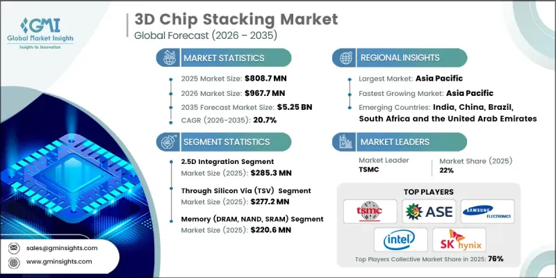
The Global 3D Chip Stacking Market was valued at USD 808.7 million in 2025 and is estimated to grow at a CAGR of 20.7% to reach USD 5.25 billion by 2035.
The market's expansion is fueled by rising demand for heterogeneous integration, cost optimization at advanced process nodes, AI and high-performance computing workload scaling, improved design flexibility, and ecosystem standardization through open interconnects. 3D chip stacking has become a cornerstone of modern semiconductor innovation, allowing multiple integrated circuit dies to be vertically stacked and interconnected within a single package. This approach reduces interconnect distances, accelerates signal transmission, enhances power efficiency, and enables a higher transistor density within compact footprints. Governments worldwide are actively supporting advanced packaging as part of industrial policies to strengthen domestic semiconductor capabilities and supply chain resilience. Technology is increasingly critical for AI accelerators, IoT devices, HPC platforms, and next-generation electronics that require high computational performance while maintaining low energy consumption and compact designs. As semiconductor ecosystems mature, 3D stacking is poised to be a key enabler of future electronics scalability and performance.
| Market Scope | |
|---|---|
| Start Year | 2025 |
| Forecast Year | 2026-2035 |
| Start Value | $808.7 Million |
| Forecast Value | $5.25 Billion |
| CAGR | 20.7% |
The 2.5D integration segment reached USD 285.3 million in 2025. 2.5D architectures place multiple dies side-by-side on an interposer, delivering high bandwidth, reduced latency, and enhanced interconnect density, which are essential for AI, HPC, networking, and graphics-intensive applications. The adoption of 2.5D integration is being reinforced by government-backed programs and R&D initiatives that accelerate interposer development and provide energy-efficient solutions for data centers and telecommunications infrastructure. Manufacturers are encouraged to invest in interposer-based 2.5D solutions to address high-bandwidth and low-latency requirements while leveraging policy support to advance next-generation semiconductor applications.
The through silicon via (TSV) segment generated USD 277.2 million in 2025. TSV technology enables vertical interconnects across stacked dies, reducing signal delay, improving power efficiency, and supporting thermal management, making it indispensable for AI accelerators, HPC systems, and data center memory stacks. Adoption of TSV is being reinforced by enterprise and government priorities to optimize chip density and performance while minimizing energy consumption and footprint. Manufacturers focusing on TSV-enabled high-performance memory and logic stacks are well-positioned to meet the increasing computational demands of AI and data-intensive applications while benefiting from government-sponsored R&D incentives.
North America 3D Chip Stacking Market accounted for 27.3% share in 2025. The region's rapid growth is supported by a mature technology ecosystem, strong R&D infrastructure, and rising demand from AI, automotive, and data center applications. Leading semiconductor companies, including Intel, NVIDIA, and AMD, are driving innovation in heterogeneous integration and high-density packaging. Government initiatives, such as funding programs for advanced packaging and 3D stacking, are enhancing domestic manufacturing capabilities and reducing dependence on overseas production. Companies in North America are scaling 3D stacking production lines in alignment with federal programs to capture high-performance computing, AI, and defense market opportunities.
Key players operating in the Global 3D Chip Stacking Market include TSMC, Intel Corporation, Samsung Electronics, Micron Technology, SK hynix, NVIDIA, Broadcom, Qualcomm, ASE Technology Holding, Amkor Technology, JCET Group, Powertech Technology Inc. (PTI), Sony Semiconductor Solutions, Toshiba (Kioxia Holdings), and Texas Instruments. Companies in the Global 3D Chip Stacking Market are strengthening their foothold by investing heavily in R&D for heterogeneous integration, high-density interposers, and TSV-enabled designs. Many firms are forming strategic alliances with foundries, memory suppliers, and AI platform developers to co-develop optimized chip architectures. Vertical integration strategies are being employed to enhance supply chain control and reduce production risks. Manufacturers are also focusing on government-backed initiatives to expand domestic manufacturing, improve thermal management solutions, and scale advanced packaging lines.
Table of Contents
Chapter 1 Methodology and Scope
- 1.1 Market scope and definition
- 1.2 Research design
- 1.2.1 Research approach
- 1.2.2 Data collection methods
- 1.3 Data mining sources
- 1.3.1 Global
- 1.3.2 Regional/Country
- 1.4 Base estimates and calculations
- 1.4.1 Base year calculation
- 1.4.2 Key trends for market estimation
- 1.5 Primary research and validation
- 1.5.1 Primary sources
- 1.6 Forecast model
- 1.7 Research assumptions and limitations
Chapter 2 Executive Summary
- 2.1 Industry 360° synopsis
- 2.2 Key market trends
- 2.2.1 Stacking architecture trends
- 2.2.2 Component trends
- 2.2.3 Technology trends
- 2.2.4 End-use industry trends
- 2.2.5 Application trends
- 2.2.6 Form factor trends
- 2.2.7 Regional trends
- 2.3 TAM Analysis, 2026 - 2035 (USD Million)
- 2.4 CXO perspectives: Strategic imperatives
Chapter 3 Industry Insights
- 3.1 Industry ecosystem analysis
- 3.1.1 Supplier landscape
- 3.1.2 Profit margin
- 3.1.3 Cost structure
- 3.1.4 Value addition at each stage
- 3.1.5 Factor affecting the value chain
- 3.1.6 Disruptions
- 3.2 Industry impact forces
- 3.2.1 Growth drivers
- 3.2.1.1 High demand for miniaturized and high-performance electronics
- 3.2.1.2 Increasing adoption of advanced packaging technologies
- 3.2.1.3 Rising use of 3D ICs in data centers and high-performance computing
- 3.2.1.4 Growth of AI, IoT, and automotive electronics applications
- 3.2.1.5 Expansion of semiconductor fabrication and foundry services
- 3.2.2 Pitfalls and challenges
- 3.2.2.1 High manufacturing complexity and cost
- 3.2.2.2 Thermal management and heat dissipation challenges
- 3.2.1 Growth drivers
- 3.3 Growth potential analysis
- 3.4 Regulatory landscape
- 3.4.1 North America
- 3.4.2 Europe
- 3.4.3 Asia Pacific
- 3.4.4 Latin America
- 3.4.5 Middle East & Africa
- 3.5 Porter’s analysis
- 3.6 PESTEL analysis
- 3.7 Technology and Innovation landscape
- 3.7.1 Current technological trends
- 3.7.2 Emerging technologies
- 3.8 Emerging Business Models
- 3.9 Compliance Requirements
Chapter 4 Competitive Landscape, 2025
- 4.1 Introduction
- 4.2 Company market share analysis
- 4.2.1 By region
- 4.2.1.1 North America
- 4.2.1.2 Europe
- 4.2.1.3 Asia Pacific
- 4.2.1.4 Latin America
- 4.2.1.5 Middle East & Africa
- 4.2.2 Market concentration analysis
- 4.2.1 By region
- 4.3 Competitive benchmarking of key players
- 4.3.1 Product portfolio comparison
- 4.3.1.1 Product range breadth
- 4.3.1.2 Technology
- 4.3.1.3 Innovation
- 4.3.2 Geographic presence comparison
- 4.3.2.1 Global footprint analysis
- 4.3.2.2 Service network coverage
- 4.3.2.3 Market penetration by region
- 4.3.3 Competitive positioning matrix
- 4.3.3.1 Leaders
- 4.3.3.2 Challengers
- 4.3.3.3 Followers
- 4.3.3.4 Niche players
- 4.3.1 Product portfolio comparison
- 4.4 Key developments, 2022-2025
- 4.4.1 Mergers and acquisitions
- 4.4.2 Partnerships and collaborations
- 4.4.3 Technological advancements
- 4.4.4 Expansion and investment strategies
- 4.4.5 Sustainability initiatives
- 4.4.6 Digital transformation initiatives
- 4.5 Emerging/ startup competitors landscape
Chapter 5 Market Estimates and Forecast, By Stacking Architecture, 2022 - 2035 (USD Million)
- 5.1 Key trends
- 5.2 Through-silicon via (TSV)
- 5.3 Micro-bump
- 5.4 Wafer-level packaging (WLP) based
- 5.5 Monolithic 3D
- 5.6 Hybrid
Chapter 6 Market Estimates and Forecast, By Component, 2022 - 2035 (USD Million)
- 6.1 Key trends
- 6.2 Memory (DRAM, NAND, SRAM)
- 6.3 Logic/processor
- 6.4 Interconnects
- 6.5 Thermal interface materials
- 6.6 Substrate & interposers
- 6.7 Others
Chapter 7 Market Estimates and Forecast, By Technology, 2022 - 2035 (USD Million)
- 7.1 Key Trends
- 7.2 2.5D integration
- 7.3 True 3D integration
- 7.4 Heterogeneous integration
- 7.5 Chiplet-based stacking
Chapter 8 Market Estimates and Forecast, By Form Factor, 2022 - 2035 (USD Million)
- 8.1 Key Trends
- 8.2 System-in-package (SiP)
- 8.3 Package-on-package (PoP)
- 8.4 3D die stack
- 8.5 Fan-out wafer level package (FOWLP)
- 8.6 Others
Chapter 9 Market Estimates and Forecast, By Application, 2022 - 2035 (USD Million)
- 9.1 Key Trends
- 9.2 High-performance computing (HPC)
- 9.3 Mobile & wearable devices
- 9.4 AI/ML accelerators
- 9.5 Storage systems
- 9.6 Baseband & RF systems
- 9.7 Sensors & MEMS
- 9.8 Others
Chapter 10 Market Estimates and Forecast, By End-use Industry, 2022 - 2035 (USD Million)
- 10.1 Key Trends
- 10.2 Consumer electronics
- 10.3 Telecommunications & networking
- 10.4 Automotive & transportation
- 10.5 Industrial & automation
- 10.6 Healthcare & medical devices
- 10.7 Aerospace & defense
- 10.8 Data centers & enterprise computing
- 10.9 Others
Chapter 11 Market Estimates and Forecast, By Region, 2022 - 2035 (USD Million)
- 11.1 Key trends
- 11.2 North America
- 11.2.1 U.S.
- 11.2.2 Canada
- 11.3 Europe
- 11.3.1 Germany
- 11.3.2 UK
- 11.3.3 France
- 11.3.4 Spain
- 11.3.5 Italy
- 11.3.6 Netherlands
- 11.4 Asia Pacific
- 11.4.1 China
- 11.4.2 India
- 11.4.3 Japan
- 11.4.4 Australia
- 11.4.5 South Korea
- 11.5 Latin America
- 11.5.1 Brazil
- 11.5.2 Mexico
- 11.5.3 Argentina
- 11.6 Middle East and Africa
- 11.6.1 Saudi Arabia
- 11.6.2 South Africa
- 11.6.3 UAE
Chapter 12 Company Profiles
- 12.1 Global Key Players
- 12.1.1 TSMC
- 12.1.2 Samsung Electronics
- 12.1.3 Intel Corporation
- 12.1.4 NVIDIA
- 12.1.5 Broadcom
- 12.2 Regional Key Players
- 12.2.1 North America
- 12.2.1.1 Micron Technology
- 12.2.1.2 Texas Instruments
- 12.2.1.3 Qualcomm
- 12.2.2 Asia Pacific
- 12.2.2.1 SK hynix
- 12.2.2.2 ASE Technology Holding
- 12.2.2.3 Amkor Technology
- 12.2.2.4 JCET Group
- 12.2.1 North America
- 12.3 Niche / Disruptors
- 12.3.1 Powertech Technology Inc. (PTI)
- 12.3.2 Sony Semiconductor Solutions
- 12.3.3 Toshiba (Kioxia Holdings)


