


 |
市场调查报告书
商品编码
1433781
半导体蚀刻设备:市场占有率分析、产业趋势/统计、成长预测(2024-2029)Semiconductor Etch Equipment - Market Share Analysis, Industry Trends & Statistics, Growth Forecasts (2024 - 2029) |
||||||
※ 本网页内容可能与最新版本有所差异。详细情况请与我们联繫。
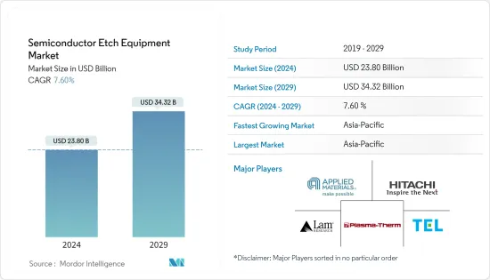
预计2024年全球半导体蚀刻设备市场规模将达238亿美元,2024-2029年预测期间复合年增长率为7.60%,2029年将达343.2亿美元。
主要亮点
- 蚀刻是半导体製造週期中的关键製程之一。该过程从半导体表面去除材料并为应用创建图案。半导体蚀刻设备市场的成长高度依赖半导体晶圆沉积和晶圆加工产业的市场开拓。
- Lam Research 表示,人工智慧、5G 和物联网等日益增长的长期推动因素是第一位的。此外,製造先进半导体装置的复杂性持续快速增加,导致所有细分市场的设备能力不断增强。
- 许多大公司正在投资扩大其製造工厂。 2022 年 2 月,博世宣布有意扩建其位于德国罗伊特林根的晶圆製造工厂。到2025年,博世计画斥资超过2.5亿欧元(2.782亿美元)扩大生产空间并建造必要的无尘室设施。这些扩张计划正在推动半导体蚀刻设备市场的成长。
- 然而,半导体是广泛交易的产品,具有复杂的製造供应链。过于复杂的海关和贸易程序、要求和做法可能会极大地扰乱半导体供应链,并造成代价高昂的壁垒,损害企业和消费者的利益。
- 由于COVID-19疫情爆发,该产业出现高额亏损和需求增加,导致供应链出现巨大缺口。由于担心汽车等关键产业对晶片的需求下降,病毒最初的传播导致晶圆代工厂关闭并降低了运转率。儘管半导体代晶圆代工厂最初预测需求增加,但产量下降导致全球半导体短缺。
半导体蚀刻设备市场趋势
导体蚀刻占最大市场占有率
- 导体蚀刻设备广泛用于形成用于半导体装置各部分的电激活材料。即使这些小型半导体结构中的微小变化也可能导致影响装置性能的电气缺陷。
- 对半导体电路小型化的需求不断增长,以及批量生产具有微小缺陷的多层薄膜迭层的需求,预计将在预测期内推动各类导体蚀刻设备的需求增加。
- 导体蚀刻有助于在半导体装置中形成电活性材料。即使这些微观结构的微小变化也会降低装置性能。此外,随着DRAM晶片的需求不断增加,许多公司正在引入导体蚀刻系统来大规模生产先进的DRAM。
- 例如,Applied Materials 的 Centris Sym3 Y 是最先进的导体蚀刻系统之一,专为 3D NAND、DRAM 和晶圆代工厂逻辑节点中的关键导体蚀刻应用而客製化。应用材料公司最先进的导体蚀刻设备专门用于 3D NAND、DRAM 和晶圆代工厂逻辑节点中的关键导体蚀刻应用。
- 此外,金属-绝缘体-金属(MIM)电容器中导体蚀刻应用的成长也是导体蚀刻的机会因素。 MIM 电容器是能源储存、讯号滤波和高频调谐应用的关键元件。
亚太地区正在经历显着成长
- 亚太地区在全球半导体晶圆代工厂中占有最显着的份额,主要企业有台积电和三星电子等。台湾、韩国、日本和中国大陆占很大比例。
- 根据半导体产业协会2021年7月的调查显示,中国已经掌握了多项晶片技术,商用半导体产业还比较年轻。儘管如此,中国政府仍在努力缩小差距,2014 年至 2030 年间在半导体领域投资超过 1,500 亿美元。在蓬勃发展的市场和政府投资的支持下,中国预计将在某些半导体细分市场变得更具竞争力。
- 此外,CNBC 于 2022 年 12 月报道称,中国正在为其半导体行业製定价值超过 1 万亿元美国(1,430 亿美元)的一揽子支持计划,标誌着朝着芯片自给自足迈出了重要一步。的技术进步。北京计划推出预计将成为其最重要的财政激励措施之一,在五年内分配,主要以补贴和税额扣抵的形式,以促进国内半导体生产和研究活动。
- 日本政府也提供财政援助,鼓励外国晶片製造商在日本建厂,为市场创造积极的成长前景。例如,2022年6月,日本经济产业省将为台积电、索尼集团和日本半导体公司在熊本县建造的半导体工厂提供高达4760亿日元(35亿美元)的补贴。Denso. 宣布计划提供该工厂的总投资预计将达到约86亿美元,其中日本政府将支持约40%的成本。
- 该地区其他国家也出现了类似的趋势。例如,2022年2月,美国半导体设备製造商Lam Research在韩国製造了下一代半导体製造核心设备。这些高选择性蚀刻机支援 Gate All around (GAA) 和 3D 沉积技术。预计它将在三星电子下一代记忆体和系统半导体的开发中发挥重要作用。
半导体蚀刻设备产业概况
由于有多家现有公司,半导体蚀刻设备市场竞争适度。本公司的品牌形象对该市场有重大影响。由于资本需求较高,新进入障碍较高,各大公司纷纷采取併购策略来扩大市场占有率。该市场的主要企业包括应用材料公司、日立高新技术美国公司、泛林研究公司和东京电子有限公司。
2022 年 6 月,AlixLab 开发了原子层蚀刻间距分裂 (APS),这是一种製造高填充半导体元件的创新方法,消除了製造过程中的多个步骤。该公司表示,这种方法使零件更便宜并且使用更少的资源。该公司还宣布已完成瑞典隆德 ProNano RISE无尘室中原子层蚀刻 (ALE) 设备的连接。
2022 年 2 月,泛林集团宣布推出全新选择性蚀刻产品线,利用突破性晶圆製造技术和新化学物质,支援晶片製造商开发环栅 (GAA) 电晶体结构。该公司的选择性蚀刻产品线由Argos、Prevos和Selis三款新产品组成,在先进逻辑和储存半导体解决方案的设计和製造方面具有强大的优势。
其他福利:
- Excel 格式的市场预测 (ME) 表
- 3 个月分析师支持
目录
第一章简介
- 研究假设和市场定义
- 调查范围
第二章调查方法
第三章执行摘要
第四章市场洞察
- 市场概况
- 产业吸引力-波特五力分析
- 供应商的议价能力
- 买方议价能力
- 新进入者的威胁
- 替代品的威胁
- 竞争公司之间敌对关係的强度
- COVID-19 市场影响评估
第五章市场动态
- 市场驱动因素
- 增加半导体製程的资本投资
- 快速的技术进步与迁移
- 市场限制因素
- 贸易担忧和半导体记忆体市场
第六章市场区隔
- 依产品类型
- 高密度蚀刻设备
- 低密度蚀刻设备
- 蚀刻膜类型
- 导体蚀刻
- 介电蚀刻
- 多晶硅蚀刻
- 按用途
- 晶圆代工厂
- MEMS
- 感应器
- 功率元件
- 按地区
- 北美洲
- 欧洲
- 亚太地区
- 其他地区
第七章 竞争形势
- 公司简介
- Applied Materials Inc.
- Hitachi High Technologies America, Inc.
- Lam Research Corporation
- Tokyo Electron Limited
- Plasma-Therm LLC
- Panasonic Corporation
- SPTS Technologies Limited(Orbotech)
- Suzhou Delphi Laser Co., Ltd
- ULVAC Inc.
第八章投资分析
第九章 市场机会及未来趋势
The Semiconductor Etch Equipment Market size is estimated at USD 23.80 billion in 2024, and is expected to reach USD 34.32 billion by 2029, growing at a CAGR of 7.60% during the forecast period (2024-2029).
Key Highlights
- Etching is one of the vital processes in a semiconductor fabrication cycle. This process eliminates the material from the surface of the semiconductor to generate patterns based on its applications. The growth of the semiconductor etch equipment market is highly dependent on the development of the semiconductor wafer deposition and wafer processing industry.
- As per Lam Research, there is a strong demand for etch and other fab equipment owing to several factors, the first being the strengthening of secular tailwinds such as AI, 5G, and IoT. Also, the complexity of manufacturing advanced semiconductor devices continues to increase at a rapid rate, as per the organization, leading to a rise in equipment capacity across all market segments.
- Many major players are investing in the expansion of their fabrication plants. In February 2022, Bosch disclosed its intention to increase the size of its wafer production facility in Reutlingen, Germany. It plans to spend more than EUR 250 million (USD 278.2 million) by 2025 to build expanded production space and the necessary clean-room amenities. Such expansion plans are fueling the growth of the semiconductor etching equipment market.
- However, semiconductors are a widely traded commodity with a complicated manufacturing supply chain. Overly complex customs and trade procedures, requirements, and practices can dramatically disrupt semiconductor supply chains, causing costly barriers that harm businesses and consumers.
- Owing to the outbreak of COVID-19, the industry was riddled with a high deficit and increasing demand, which has led to a significant supply chain gap. The initial spread of the virus led to the shutting down or the reduction of foundry capacity utilization, fearing the decreasing demand for the chips across major sectors, like automotive. The diminished output led to a global shortage of semiconductors as the demand increased despite the initial estimates by semiconductor foundries.
Semiconductor Etch Equipment Market Trends
Conductor Etching to Hold the Largest Market Share
- Conductor etching equipment is used widely to shape the electrically activated materials used in different parts of the semiconductor device. Even a minimal variation in these small semiconductor structures can lead to an electrical fault impacting the device's performance.
- The increasing demand for miniaturization of semiconductor circuits is anticipated to catalyze the ever-increasing demand for different types of conductor etching equipment, along with the need for high production of multi-film stacks with a minor fault during the forecasted period.
- Conductor etching helps in shaping the electrically active materials of a semiconductor device. The presence of even a slight variation in these miniature structures can degrade device performance. Moreover, with the growing demand for DRAM chips, many players have introduced conductor etch systems for the volume production of advanced DRAMs.
- For instance, Centris Sym3 Y is one of the most advanced conductor etch systems by Applied Materials and is tailored to critical conductor etch applications in 3D NAND, DRAM, and foundry-logic nodes. It enables chipmakers to precisely pattern and shape ever-smaller features in state-of-the-art memory and logic chips.
- Moreover, the growth of usage of conductor etching in Metal Insulator Metal (MIM) capacitors also acts as an opportunity factor for Conductor Etching. MIM capacitors are important components for energy storage, signal filtering, and high-frequency tuning applications.
Asia-Pacific to Witness Significant Growth
- The Asia-Pacific region has the most prominent share of global semiconductor foundries, with major companies such as TSMC, Samsung Electronics, etc. Taiwan, South Korea, Japan, and China have a significant market share in the region.
- According to a survey conducted by the Semiconductor Industry Association in July 2021, China mastered several chip technologies, and its commercial semiconductor industry is still relatively young. Still, the Chinese government is trying to close the gap, investing more than USD 150 billion in semiconductors between 2014 and 2030. Supported by booming markets and these government investments, China is poised to become increasingly competitive in some semiconductor market segments.
- Moreover, as per a report by CNBC in December 2022, China is working on a more than CNY 1 trillion (USD 143 billion) support package for its semiconductor industry, in a major step toward self-sufficiency in chips and to counter the United States moves aimed at slowing its technological advances. Beijing has planned to roll out what is expected to be one of its most significant fiscal incentive packages, allocated over five years, mainly as subsidies and tax credits to strengthen semiconductor production and research activities at home.
- Also, Japan's government is offering financial aid to encourage foreign chip makers to build plants in Japan, which is creating a positive growth outlook for the market. For instance, in June 2022, Japan's Ministry of Economy, Trade and Industry (METI) announced plans to offer subsidies worth up to JPY 476 billion (USD 3.5 billion) for a semiconductor plant being built in Kumamoto Prefecture by Taiwan Semiconductor Manufacturing Co. (TSMC), Sony Group and Denso. Total investment in the plant was expected to reach around USD 8.6 billion, with Japan's government supporting about 40% of the costs.
- A similar trend has also been observed across other countries in the region. For instance, in February 2022, Lam Research, a US semiconductor equipment company, manufactured next-generation core equipment for semiconductor manufacturing in South Korea. These highly selective etching devices support Gate All Around (GAA) and 3D stacking technology. The new equipment is expected to play an important role in developing Samsung Electronics' next-generation memory and system semiconductors.
Semiconductor Etch Equipment Industry Overview
The Semiconductor Etch Equipment Market is moderately competitive owing to the presence of some established players. The brand identity associated with the companies has a major influence in this market. As the barrier for the new entrants is high in the market due to the high capital incorporated, major players are adopting mergers and acquisition strategies to gain more market share. Some major players operating in the market include Applied Materials Inc., Hitachi High Technologies America, Inc., Lam Research Corporation, and Tokyo Electron Limited.
In June 2022, AlixLab developed a new, innovative method for manufacturing semiconductor components with a high degree of packing, eliminating several steps in the manufacturing process - Atomic Layer Etch Pitch Splitting (APS). According to the company, the method makes the components cheaper and less resource-intensive. The company also announced the completion of the Atomic Layer Etch (ALE) equipment hook-up in its clean room at ProNano RISE in Lund, Sweden.
In February 2022, Lam Research Corp. announced a new suite of selective etch products that apply breakthrough wafer fabrication techniques and novel chemistries to support chipmakers in developing gate-all-around (GAA) transistor structures. Composed of three new products, Argos, Prevos, and Selis, the company's selective etch portfolio provides a powerful advantage in the design and manufacture of advanced logic and memory semiconductor solutions.
Additional Benefits:
- The market estimate (ME) sheet in Excel format
- 3 months of analyst support
TABLE OF CONTENTS
1 INTRODUCTION
- 1.1 Study Assumptions and Market Definition
- 1.2 Scope of the Study
2 RESEARCH METHODOLOGY
3 EXECUTIVE SUMMARY
4 MARKET INSIGHTS
- 4.1 Market Overview
- 4.2 Industry Attractiveness - Porter's Five Forces Analysis
- 4.2.1 Bargaining Power of Suppliers
- 4.2.2 Bargaining Power of Buyers
- 4.2.3 Threat of New Entrants
- 4.2.4 Threat of Substitute Products
- 4.2.5 Intensity of Competitive Rivalry
- 4.3 Assessment of the Impact of COVID-19 on the Market
5 MARKET DYNAMICS
- 5.1 Market Drivers
- 5.1.1 Increase in Capital Spending on Semiconductor Processing
- 5.1.2 Rapid Technological Advances and Transition
- 5.2 Market Restraints
- 5.2.1 Trade Uncertainties and Semiconductor Memory Markets
6 MARKET SEGMENTATION
- 6.1 By Product Type
- 6.1.1 High-density Etch Equipment
- 6.1.2 Low-density Etch Equipment
- 6.2 By Etching Film Type
- 6.2.1 Conductor Etching
- 6.2.2 Dielectric Etching
- 6.2.3 Polysilicon Etching
- 6.3 By Application
- 6.3.1 Foundries
- 6.3.2 MEMS
- 6.3.3 Sensors
- 6.3.4 Power Devices
- 6.4 By Geography
- 6.4.1 North America
- 6.4.2 Europe
- 6.4.3 Asia-Pacific
- 6.4.4 Rest of the World
7 COMPETITIVE LANDSCAPE
- 7.1 Company Profiles
- 7.1.1 Applied Materials Inc.
- 7.1.2 Hitachi High Technologies America, Inc.
- 7.1.3 Lam Research Corporation
- 7.1.4 Tokyo Electron Limited
- 7.1.5 Plasma-Therm LLC
- 7.1.6 Panasonic Corporation
- 7.1.7 SPTS Technologies Limited (Orbotech)
- 7.1.8 Suzhou Delphi Laser Co., Ltd
- 7.1.9 ULVAC Inc.
8 INVESTMENT ANALYSIS
9 MARKET OPPORTUNITIES AND FUTURE TRENDS
 2025年全球半导体蚀刻设备市场报告2025年蚀刻机全球市场报告
 全球硅蚀刻零件市场:市场占有率和排名、总收入和需求预测(2025-2031)
 2025-2033 年半导体介质蚀刻设备市场报告(按类型(湿蚀刻设备、干蚀刻设备)、应用(代工厂、整合装置製造商 (IDM))和地区
 半导体蚀刻设备市场规模、份额、成长分析、按产品类型、蚀刻膜类型、应用、地区 - 产业预测,2025-2032
 亚太地区半导体蚀刻设备:市场占有率分析、产业趋势、成长预测(2025-2030)全球电介质蚀刻市场:市场占有率分析、产业趋势、成长预测(2025-2030)北美半导体蚀刻设备:市场占有率分析、行业趋势和成长预测(2025-2030 年)欧洲半导体蚀刻设备:市场占有率分析、产业趋势/统计、成长预测(2025-2030)
 半导体干蚀刻系统市场,按蚀刻技术、应用、最终用途、国家和地区 - 2024-2032 年行业分析、市场规模、市场份额和预测