


 |
市场调查报告书
商品编码
1685905
半导体封装:市场占有率分析、产业趋势与统计、成长预测(2025-2030 年)Semiconductor Packaging - Market Share Analysis, Industry Trends & Statistics, Growth Forecasts (2025 - 2030) |
||||||
※ 本网页内容可能与最新版本有所差异。详细情况请与我们联繫。
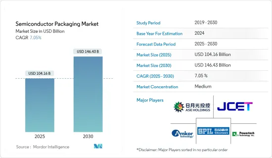
半导体封装市场规模预计在 2025 年为 1,041.6 亿美元,预计到 2030 年将达到 1,464.3 亿美元,预测期内(2025-2030 年)的复合年增长率为 7.05%。
半导体封装是指塑胶、陶瓷、金属或玻璃製成的外壳,内含一个或多个离散半导体装置或积体电路。封装对于保护电子系统免受高频噪音辐射、静电放电、机械损坏和冷却至关重要。
高效能运算、资料中心网路和自动驾驶汽车正在推动该市场的采用率并加速技术进步。目前趋势是云端运算、边缘运算和设备层面拥有更多的运算资源。此外,通讯业和基础设施产业的高端性能应用和人工智慧(AI)的成长也推动了所研究市场的发展。
随着前端节点的缩小,设计成本变得越来越重要。先进封装 (AP) 解决方案透过提高系统效能同时降低成本、提供更低的延迟、更高的频宽和更高的功率效率来帮助解决这些问题。
职场的数位化位化、远端工作和远端工作趋势的出现以及消费者对电子设备日益增长的偏好,正在推动对半导体设备的需求,从而可以释放广泛的新机会。随着半导体装置的成长不断加速,先进的封装技术提供了数位化时代所需的尺寸和处理能力。
世界各国政府正透过降低门槛、增加生产和研发补贴等方式加大对半导体产业的支持。例如,韩国承诺投入高达 4,560 亿美元的私人投资来打造全球最大的晶片中心,彰显其主导该产业的雄心壮志。
同时,韩国政府推出大规模扶持半导体产业措施,总额高达26兆韩元(约191亿美元)。该计划涵盖财政援助、基础设施建设、研发和对中小企业的针对性支持。韩国目前正在首尔郊外建造一个“巨型晶片丛集”,预计将成为全球最大的半导体中心,并成为创造许多新的就业机会的关键驱动力。
设计、开发和安装半导体封装设备以满足汽车、家电、医疗保健、IT 和通讯、航太和国防等各行业的需求,需要大量的前期投资。这可能会限制半导体封装市场的成长。
此外,每个国家的国防预算都受到通货膨胀、经济成长、政府支出重点以及全球贸易和地缘政治动态等关键宏观经济因素的影响。
2023年3月,拜登总统提案了美国史上最大的和平时期国防预算,总额达8,860亿美元。该预算包括士兵薪资增加5.2%以及创纪录的研发累计。在俄罗斯在乌克兰采取行动的背景下,增加军事装备支出的必要性进一步凸显。
根据美国预算办公室预测,美国国防支出将持续增加,直至2033年。 2023年,美国国防支出预计将达7,460亿美元,到2033年将增加至1.1兆美元。
半导体封装市场趋势
通讯和电讯业作为最终用户正在快速成长
- 网路和连接性的演变是显而易见的。我们已经从透过有线基础设施进行语音和视讯讯号的基本交换发展到目前透过无线基础设施进行多媒体和大量资料的交换。
- 半导体在通讯基础设施中至关重要,处理从资料撷取和编码到加密、传输以及最终呈现给使用者的各种任务。 5G 技术预示着 IT 和通讯网路及设备的重大飞跃,提供更快的速度和重点的极低延迟。这种降低的延迟对于云端游戏和 VR 内容流等应用尤其重要。因此,通讯和通讯业对半导体的需求增加预计将推动半导体封装市场的成长。
- 同样,美国政府在2024年2月拨款4,200万美元,用于促进美国的无线创新。这笔资金将用于一个涉及美国通讯业者、国际通讯业者、领先大学和设备供应商的合作计划。该倡议旨在达拉斯技术走廊建立一个测试、评估和研发中心,并在华盛顿特区设立一个卫星设施。这些设施的主要重点是测试网路效能、确保互通性、加强安全措施以及带头研究新的测试方法。
- 同样在 2023 年 4 月,爱立信宣布打算与加拿大政府合作,五年内投资 4.7 亿加元(3.4544 亿美元)。该投资主要针对 6G、5G Advanced、人工智慧、Cloud RAN 和核心网路等技术的研发。该倡议的目的是促进该地区通讯的发展并支持研究设施的发展。这些投资将推动广泛应用于通讯产业的半导体装置需求激增,进一步促进市场成长。
- 2024年,新兴通讯业将迎来技术进步与策略市场发展的结合。采用创新、先进的半导体解决方案将在这一转变中发挥关键作用,满足日益增长的连接性和速度需求,同时解决安全性、永续性和客製化用户体验等关键因素。随着技术的不断进步,电讯和半导体技术的合作预计将对全球数位格局产生重大影响。
- 云端技术的日益普及、资料中心的不断普及以及 5G 技术的日益普及,进一步推动了半导体封装市场的成长。全球资料中心和云端运算市场的扩张预计将刺激资料储存的需求,进一步推动市场成长。例如,根据Cloudscene的数据,截至2024年3月,美国拥有5,381个资料中心,比世界上任何其他国家都多。
台湾可望占较大市场占有率
- 台湾是台积电 (台湾半导体製造公司) 和联华电子 (联合微电子) 等主要半导体製造商的所在地。这些公司的强大影响力创造了对先进封装解决方案的需求。
- 例如,2024年3月,台积电为了满足AI晶片需求,在台湾北部、中部和南部启动大规模扩建。此次扩建包括增加一个 2 奈米晶圆厂和一个最先进的封装设施。台积电甚至表示,可能需要投资 8 到 10 个设施来支援台湾即将推出的 1 奈米技术。
- 对人工智慧晶片的不断增长的需求推动了对基板晶圆上晶片(CoWoS)等先进封装技术的需求。为了满足日益增长的需求,台积电正在扩建位于台湾科学园区中心竹南的先进封装工厂。该公司计划今年开始整合工具和生产线。此外,嘉义先进封装工厂的建设也计划于今年开始。
- 台湾数位经济的成长满足了客户需求并支援高效能运算(HPC)、人工智慧(AI)和行动应用等产品,为台湾半导体封装市场创造了机会,该市场使用堆迭在一起的半导体晶粒来实现更小的晶片尺寸和更高性能的应用。 GSMA预测,2025年,全球超过50%的行动网路连线将由台湾的5G技术支援。
- 例如,2023 年 5 月,合约晶片製造商台湾半导体製造股份有限公司 (TSMC) 宣布计划在 2024 年建造七座新工厂,以增强其全球竞争力。这些设施包括台湾的三座晶圆厂、两座封装厂和海外的两座晶圆厂。此次扩张是对全球对高效能运算设备和智慧型手机的需求的策略性响应。该先进封装工厂预计将于2023年在台湾中部破土动工。
- 此外,嘉义工厂预计将于今年稍后开始运作,计划到 2026 年部署晶圆上晶片 (CoWoS) 和小外形积体电路 (SoIC) 技术。 2024 年 6 月,台湾半导体公司台积电面临对其先进技术的飙涨需求。苹果、Nvidia 等主要企业的台积电生产订单已全部预订,订单将延续到 2026 年。
- 为了因应此次涨价,台积电希望将 3nm 价格上调 5%,但先进封装价格明年可能还会上涨 10% 至 20%。台积电3nm产品线包括N3、N3E、N3P,以及新增加的N3X和N3A。虽然它代表了对原始 N3 技术的改进,但去年第四季开始量产的 N3E 是为 AI 加速器、高阶智慧型手机和资料中心而设计的。
- 半导体作为医疗保健行业的工具和设备有多种用途。超音波技术的日益广泛应用推动了该国半导体封装的使用,这与医疗保健数位化以及该国医院中电子设备的使用日益广泛相一致。在台湾,製造商主要透过为跨国公司契约製造的方式,生产和出口价格分布医疗设备。
- 2024年1月,国际贸易局引用台湾经济部的资料,强调台湾医疗设备产量激增。该部宣布,2023 年国内生产总值将达到 8,928,333 美元,呈现持续上升趋势,显示市场成长轨迹良好。
半导体封装市场概况
半导体封装市场半固体,主要企业包括日月光科技控股、安靠科技、江苏长江、长电科技、硅品精准工业和力成科技股份有限公司。市场参与者正在采用合作和收购等策略来加强其产品供应并获得永续的竞争优势。
- 2024年4月,三星AVP团队订单NVIDIA AI晶片的先进封装合同,从而实现未来高频宽记忆体晶片的供应。三星电子的AVP团队将负责为NVIDIA的AI处理器的封装提供内插器和2.5D封装技术。不过,这些处理器使用的HBM和GPU晶片将来自其他供应商。 2.5D封装技术可以将CPU、GPU、HBM等晶片水平整合在内插器上。
- 2023年12月,长电科技在江苏省江阴市开设半导体封测博物馆。该博物馆是展示积体电路封装和测试领域的专业设施。这标誌着长电科技推动封测产业迈出新的一步。该博物馆是江阴积体电路领域科技发展的标誌性工程,也是展示封测产业成果的平台。
其他福利
- Excel 格式的市场预测 (ME) 表
- 3 个月的分析师支持
目录
第 1 章 简介
- 研究假设和市场定义
- 研究范围
第二章调查方法
第三章执行摘要
第四章 市场洞察
- 市场概况
- 产业吸引力-波特五力分析
- 供应商的议价能力
- 买家的议价能力
- 新进入者的威胁
- 替代品的威胁
- 竞争对手之间的竞争
- 产业价值链分析
- COVID-19 的副作用和其他宏观经济因素将如何影响市场
第五章 市场动态
- 市场驱动因素
- 各行业对半导体装置的消费不断增加
- 新兴国家有利的政府法规和政策
- 市场限制
- 初期投资高,半导体IC设计复杂
第六章 市场细分
- 按包装平台
- 先进封装
- 覆晶
- SIP
- 2.5D/3D
- 内建晶粒
- 扇入晶圆级封装 (FI-WLP)
- 扇出型晶圆级封装 (FO-WLP)
- 传统包装
- 先进封装
- 按最终用户产业
- 消费性电子产品
- 航太和国防
- 医疗设备
- 通讯和电讯
- 汽车
- 能源与照明
- 按地区
- 美国
- 中国
- 台湾
- 韩国
- 日本
- 欧洲
- 拉丁美洲
- 中东和非洲
第七章 竞争格局
- 公司简介
- ASE Technology Holding Co. Ltd
- Amkor Technology
- Jiangsu Changjiang Electronics Technology Co. Ltd(JCET)
- Siliconware Precision Industries Co. Ltd
- Powertech Technology Inc.
- Tianshui Huatian Technology Co. Ltd
- Fujitsu Semiconductor Ltd
- UTAC Holdings Ltd
- Chipmos Technologies Inc.
- Chipbond Technology Corporation
- Intel Corporation
- Samsung Electronics Co. Ltd
- Unisem(M)Berhad
- Interconnect Systems Inc.(ISI)
第八章投资分析
第九章:市场的未来
The Semiconductor Packaging Market size is estimated at USD 104.16 billion in 2025, and is expected to reach USD 146.43 billion by 2030, at a CAGR of 7.05% during the forecast period (2025-2030).
Semiconductor packaging refers to a casing that contains one or more discrete semiconductor devices or integrated circuits made up of plastic, ceramic, metal, or glass casing. Packaging is crucial for protecting an electronic system from radio frequency noise emission, electrostatic discharge, mechanical damage, and cooling.
High-performance computing, data center networking, and autonomous vehicles are pushing the adoption rates for the market studied and accelerating its technological evolution. The trend is to have more enormous computing resources at the cloud, edge computing, and device levels. The advancements in the market studied are also possible due to the growth in high-end performance applications and artificial intelligence (AI) in the telecom and infrastructure industry.
As the front-end node becomes smaller, design cost becomes increasingly important. Advanced packaging (AP) solutions aid in solving these problems by reducing the cost while enhancing system performance and offering lower latency, increased bandwidth, and power efficiency.
The increasing digitization of the workplace, the emergence of remote working and remote operation trends, and the growing consumer preference for electronics have increased the demand for semiconductor devices capable of unlocking a wide range of new opportunities. As the growth of semiconductor devices continues to accelerate, advanced packaging technologies provide the size and processing power necessary for the digitized era.
Global governments are increasingly supporting the semiconductor industry by lowering barriers and ramping up production, research, and development subsidies. For instance, South Korea committed a staggering USD 456 billion in private investments to construct the world's largest chip center, underlining its ambitions for industry dominance.
In tandem with this, the South Korean government rolled out an extensive support initiative for its semiconductor industry, valued at KRW 26 trillion (approximately USD 19.1 billion). This program spans financial aid, infrastructure development, R&D, and targeted assistance for its SMEs. Just outside Seoul, South Korea is currently in the works of creating a "mega chip cluster," which is projected to become the largest semiconductor hub globally and a key driver in creating numerous new employment opportunities.
A significantly high initial investment is required in designing, developing, and setting up semiconductor packaging units as per the requirements of different industries such as automotive, consumer electronics, healthcare, IT and telecommunication, and aerospace and defense. This can restrict the growth of the semiconductor packaging market.
Moreover, the defense budgets of various countries are significantly influenced by major macroeconomic factors such as inflation, economic growth, government spending priorities, and global trade and geopolitical dynamics.
In March 2023, President Joe Biden proposed the largest peacetime US defense budget, totaling USD 886 billion. This budget notably included a 5.2% pay raise for troops and marked the highest-ever allocation for research and development. The backdrop of Russia's actions in Ukraine further underscored the need for increased spending on munitions.
As per the US Congressional Budget Office, the United States is set to witness a consistent rise in defense spending, with projections extending until 2033. In 2023, the United States spent USD 746 billion on defense, with forecasts indicating a climb to USD 1.1 trillion by 2033.
Semiconductor Packaging Market Trends
The Communication and Telecom Segment to be the Fastest Growing End User
- The evolution in networking and connectivity is quite visible. It has evolved from the basic exchange of voice and visual signals through wired infrastructure to the current state of exchanging multimedia and large volumes of data through wireless infrastructure.
- Semiconductors are pivotal in telecom infrastructure, handling tasks from capturing and encoding data to encryption, transmission, and, ultimately, user presentation. 5G technology heralds a significant leap in telecommunication networks and devices, offering notably faster speeds than its predecessors and, crucially, boasting remarkably low latency. This reduced latency is especially vital for applications like cloud gaming and VR content streaming. Thus, the increasing demand for semiconductors in the communication and telecom industry is expected to propel the growth of the semiconductor packaging market.
- Similarly, in February 2024, the US government allocated a substantial USD 42 million toward fostering wireless innovation within the nation. This funding was earmarked for a collaborative project involving US carriers, international counterparts, leading universities, and equipment suppliers. The initiative aimed to set up a testing, evaluation, and R&D center in the Dallas Technology Corridor, complemented by a satellite facility in Washington, DC. The primary focus of these facilities would be testing network performance, ensuring interoperability, enhancing security measures, and spearheading research into novel testing methodologies.
- Similarly, in April 2023, Ericsson expressed its intention to collaborate with the Canadian government and invest CAD 470 million (USD 345.44 million) over five years. This investment was directed toward researching and developing technologies such as 6G, 5G advanced, artificial intelligence, Cloud RAN, and core networks. The objective of this initiative was to foster the growth of the telecommunications industry in the region and support the development of research facilities. These investments were poised to surge the demand for semiconductor devices due to their widespread use in the telecommunications industry, further bolstering the market's growth.
- In 2024, the telecommunications industry across emerging nations showcased a mix of technological advancements and strategic market development. Incorporating innovative and advanced semiconductor solutions played a vital role in this shift, meeting the increasing needs for connectivity and speed and addressing crucial elements like security, sustainability, and customized user experience. With ongoing progress, the collaboration between telecom and semiconductor technologies is expected to significantly influence the global digital landscape.
- The growing adoption of cloud technology, increasing penetration of data centers, and rising popularity of 5G technology are further bolstering the growth of the semiconductor packaging market. The increasing expansion of the data center and cloud market worldwide is expected to fuel the demand for data storage, further propelling the market's growth. For instance, according to Cloudscene, as of March 2024, there were 5,381 data centers in the United States, the most of any country worldwide.
Taiwan is Expected to Hold Significant Market Share
- Taiwan is home to some of the largest semiconductor manufacturers, such as TSMC (Taiwan Semiconductor Manufacturing Company) and United Microelectronics Corporation (UMC). The robust presence of these companies creates a demand for advanced packaging solutions.
- For instance, in March 2024, TSMC, considering the surging demand for AI chips, launched a significant expansion across Northern, Central, and Southern Taiwan. This expansion encompasses the introduction of 2-nanometer fabs and cutting-edge packaging plants. TSMC had even hinted at the potential need to invest in eight to ten facilities to support the upcoming 1-nanometer technology in Taiwan.
- The rising demand for AI chips is fueling the necessity for advanced packaging technologies, such as CoWoS (Chip-on-Wafer-on-Substrate). To meet this escalating demand, TSMC is ramping up its advanced packaging facilities in Zhunan, located in the heart of Taiwan's Science Park. The company will kick off tool-in and production line integration this year. Additionally, construction for an advanced packaging facility in Chiayi is slated to begin this year.
- The growth of Taiwan's digital economy to meet customers' needs and support products such as high-performance computing (HPC), artificial intelligence (AI), and mobile applications has created an opportunity for the semiconductor packaging market in Taiwan as its use in combining semiconductor dies on top of each other for miniaturized and high-performance applications of semiconductor chips. GSMA's forecast predicts that by 2025, over 50% of global mobile internet connections will be powered by 5G technology in Taiwan.
- For instance, in May 2023, Taiwan Semiconductor Manufacturing Co. (TSMC), the contract chip manufacturer, announced its plans to construct seven new facilities in 2024 to enhance its global competitive edge. These facilities would include three wafer plants, two packaging factories in Taiwan, and two overseas wafer plants. This expansion was a strategic response to the worldwide appetite for high-performance computing devices and smartphones. Construction commenced on an advanced packaging factory in Central Taiwan in 2023.
- Additionally, a facility in Chiayi is set to kick off later this year, with plans to roll out Chip-on-Wafer-on-Substrate (CoWoS) and small outline integrated circuit (SoIC) technologies by 2026. In June 2024, Taiwan's semiconductor company, TSMC, grappled with a soaring demand for its advanced technology. Key players like Apple and NVIDIA have fully booked TSMC's production, with orders stretching into 2026.
- In response to this surge, TSMC is eyeing a 5% hike in its 3 nm prices, while its advanced packaging rates could see a steeper rise of 10% to 20% in the coming year. TSMC's 3 nm lineup comprises N3, N3E, and N3P, alongside newer additions N3X and N3A. While the original N3 technology undergoes enhancements, N3E, which commenced mass production in Q4 of the previous year, is designed for AI accelerators, premium smartphones, and data centers.
- Semiconductors are used in various ways as tools and equipment in the healthcare industry. The expanding use of ultrasound technology encourages the use of semiconductor packaging in the country, which is in line with the growth of healthcare digitalization and electronic device usage in the country's hospitals. In Taiwan, manufacturers significantly focus on producing and exporting mid-to-low-end medical equipment through contract manufacturing for multinational companies.
- In January 2024, the International Trade Administration highlighted a surge in the country's medical device production by data from the Taiwan Ministry of Economic Affairs. The ministry published that the total local production in 2023 reached USD 8,928,333, marking a consistent upward trend and showing a promising growth trajectory for the market.
Semiconductor Packaging Market Overview
The semiconductor packaging market is semi-consolidated with the presence of significant players like ASE Technology Holding Co. Ltd, Amkor Technology, Jiangsu Changjiang, Electronics Technology Co. Ltd (JCET), Siliconware Precision Industries Co. Ltd, and Powertech Technology Inc. Players in the market are adopting strategies, such as partnerships and acquisitions, to enhance their product offerings and gain sustainable competitive advantage.
- In April 2024, Samsung's AVP team received an order for advanced packaging for NVIDIA's AI chip, allowing for the future supply of high-bandwidth memory chips. The AVP team at Samsung Electronics will be responsible for providing interposer and 2.5D packaging technology for packaging NVIDIA's AI processors. However, the HBM and GPU chips used in these processors will come from other suppliers. The 2.5D packaging technology allows for the horizontal integration of chips such as CPUs, GPUs, and HBMs on an interposer.
- In December 2023, JCET opened the Semiconductor Packaging and Test Museum in Jiangyin, Jiangsu Province. The museum is a dedicated establishment that exhibits the realm of integrated circuit packaging and testing. It signifies a fresh endeavor by JCET to propel the packaging and testing industry. The museum acts as a prominent symbol for fostering science and technology in the IC sector within Jiangyin while also serving as a platform to showcase the accomplishments of the packaging and testing industry.
Additional Benefits:
- The market estimate (ME) sheet in Excel format
- 3 months of analyst support
TABLE OF CONTENTS
1 INTRODUCTION
- 1.1 Study Assumptions and Market Definition
- 1.2 Scope of the Study
2 RESEARCH METHODOLOGY
3 EXECUTIVE SUMMARY
4 MARKET INSIGHTS
- 4.1 Market Overview
- 4.2 Industry Attractiveness - Porter's Five Forces Analysis
- 4.2.1 Bargaining Power of Suppliers
- 4.2.2 Bargaining Power of Buyers
- 4.2.3 Threat of New Entrants
- 4.2.4 Threat of Substitutes
- 4.2.5 Intensity of Competitive Rivalry
- 4.3 Industry Value Chain Analysis
- 4.4 Impact of COVID-19 Aftereffects and Other Macroeconomic Factors on the Market
5 MARKET DYNAMICS
- 5.1 Market Drivers
- 5.1.1 Growing Consumption of Semiconductor Devices Across Industries
- 5.1.2 Favorable Government Policies and Regulations in Developing Countries
- 5.2 Market Restraints
- 5.2.1 High Initial Investment and Increasing Complexity of Semiconductor IC Designs
6 MARKET SEGMENTATION
- 6.1 By Packaging Platform
- 6.1.1 Advanced Packaging
- 6.1.1.1 Flip Chip
- 6.1.1.2 SIP
- 6.1.1.3 2.5D/3D
- 6.1.1.4 Embedded Die
- 6.1.1.5 Fan-in Wafer Level Packaging (FI-WLP)
- 6.1.1.6 Fan-out Wafer Level Packaging (FO-WLP)
- 6.1.2 Traditional Packaging
- 6.1.1 Advanced Packaging
- 6.2 By End-user Industry
- 6.2.1 Consumer Electronics
- 6.2.2 Aerospace and Defense
- 6.2.3 Medical Devices
- 6.2.4 Communications and Telecom
- 6.2.5 Automotive Industry
- 6.2.6 Energy and Lighting
- 6.3 By Geography
- 6.3.1 United States
- 6.3.2 China
- 6.3.3 Taiwan
- 6.3.4 South Korea
- 6.3.5 Japan
- 6.3.6 Europe
- 6.3.7 Latin America
- 6.3.8 Middle East and Africa
7 COMPETITIVE LANDSCAPE
- 7.1 Company Profiles
- 7.1.1 ASE Technology Holding Co. Ltd
- 7.1.2 Amkor Technology
- 7.1.3 Jiangsu Changjiang Electronics Technology Co. Ltd (JCET)
- 7.1.4 Siliconware Precision Industries Co. Ltd
- 7.1.5 Powertech Technology Inc.
- 7.1.6 Tianshui Huatian Technology Co. Ltd
- 7.1.7 Fujitsu Semiconductor Ltd
- 7.1.8 UTAC Holdings Ltd
- 7.1.9 Chipmos Technologies Inc.
- 7.1.10 Chipbond Technology Corporation
- 7.1.11 Intel Corporation
- 7.1.12 Samsung Electronics Co. Ltd
- 7.1.13 Unisem (M) Berhad
- 7.1.14 Interconnect Systems Inc. (ISI)
8 INVESTMENT ANALYSIS
9 FUTURE OF THE MARKET
 半导体原型製作和封装市场分析及预测(至 2034 年):类型、产品、服务、技术、应用、材料类型、组件、流程、最终用户、设备
 全球 3D 半导体封装市场:未来预测(至 2032 年)—材料、技术、最终用户和地区分析
 3-D TSV:关键问题洞察与市场分析
 高密度封装(MCM、MCP、SIP、3D-TSV):市场分析与技术趋势
 2025年先进晶片封装全球市场报告2025年全球3D半导体封装市场报告
 半导体先进封装市场(按平台、材料类型、组件、间距、应用和最终用途行业)- 全球预测,2025 年至 2030 年2025年全球四方扁平封装市场报告先进晶片封装市场(按封装类型和地区)
 日本半导体封装市场规模、份额、趋势及预测(按类型、封装材料、技术、最终用户和地区),2025 年至 2033 年