


 |
市场调查报告书
商品编码
1630179
半导体晶圆抛光研磨设备:市场占有率分析、产业趋势、成长预测(2025-2030)Semiconductor Wafer Polishing and Grinding Equipment - Market Share Analysis, Industry Trends & Statistics, Growth Forecasts (2025 - 2030) |
||||||
价格
※ 本网页内容可能与最新版本有所差异。详细情况请与我们联繫。
简介目录
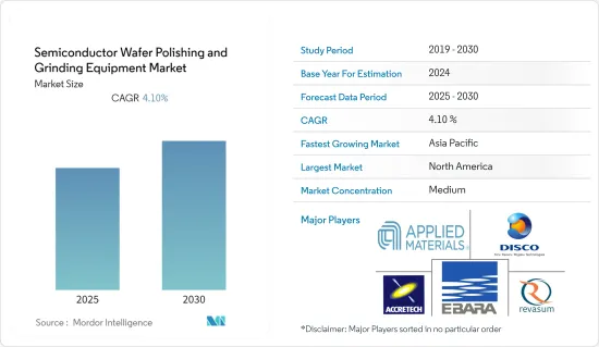
预计半导体晶圆抛光和研磨设备市场在预测期内的复合年增长率为4.1%。
主要亮点
- 对MEMS、IC製造、光学和化合物半导体的需求增加将推动半导体装置的平坦化。在当前的市场场景下,笔记型电脑、智慧型手机、电脑等几乎所有电子设备都采用硅IC和其他晶圆相关封装,因此对先进研磨和抛光设备的需求不断增加。
- 根据SEMI统计,2022年第二季全球整体硅晶圆出货量达37.04亿平方英寸,较去年同期的35.34亿平方英吋成长5%。这样的市场格局预计将在不久的将来为市场带来一些新的机会。
- 此外,对电子设备小型化的需求不断增长(由于对更薄且功耗更低的晶圆的需求)预计将在预测期内推动半导体晶圆抛光和研磨设备市场的若干进步。
- 然而,蚀刻技术的最新进展与抛光技术相比具有更多优势,影响了对抛光设备的需求。此外,使用传统 CMP(化学机械抛光)技术进行抛光来去除局部缺陷可以保留表面形貌,这使得参与晶圆回收的製造商和服务供应商变得极其困难。
- 2020 年初,COVID-19 严重扰乱了世界各地的半导体供应链和生产,尤其是在中国。然而,疫情导致的数位化趋势日益增强,预计将增加对半导体元件的需求,并对未来市场产生正面影响。
半导体晶圆抛光研磨设备市场趋势
消费性电子产品消费的增加预计将对市场产生正面影响
- 智慧型手机和平板电脑等家用电子电器的技术进步以及智慧家居设备和穿戴式装置领域的发展正在推动对小型积体电路的需求。因此,在半导体晶圆製造过程中发挥重要作用的晶圆抛光和研磨设备的需求不断增加。
- 半导体材料市场的整体需求是由智慧型手机、消费性电子和汽车等应用所推动的。这些产业受到无线技术(5G)、人工智慧等技术转型的启发。此外,物联网(IoT)设备的成长趋势预计将迫使半导体产业投资该设备以实现智慧产品。
- 所有智慧型手机均由 SoC(系统单晶片)构成,这是一种包含电脑或其他电子系统的全部或大部分组件的积体电路。 SoC 晶片通常使用金属氧化物半导体 (MOS) 技术製造,并发送到晶圆製造工厂,在封装和测试之前对晶圆进行抛光和研磨,以创建 SoC 晶片。因此,智慧型手机渗透率的不断提高预计将对市场产生积极影响。
- 此外,微电子设备正在向消费性电子产品领域取得重大进展。微电子学的应用正在帮助设计穿戴在人体上的装置。透过这种实现,腕带、穿戴式显示器、穿戴式医疗保健产品等旨在监测个人健康。化学机械抛光是硅片製造和加工的关键技术,有助于实现尖端的微电子装置和电子机械系统(MEMS)。
- 此外,高性能且轻巧的电子设备正在兴起。因此,为了在此类设备中安装更多元件,半导体必须做得更小、封装更紧密、更轻,以便为其他元件腾出空间。因此,晶片抛光是半导体製造的重要製程。
北美预计将占据很大份额
- 多年来,美国半导体产业在全球销售市场占有率上一直保持主导地位。该国也是半导体封装领域的领先创新者之一,拥有遍布各州的众多晶圆製造厂。该地区的主要无厂半导体公司包括 Broadcom、AMD、Qualcomm、Apple、Marvell、Xilinx 和 NVIDIA。
- 随着无厂半导体公司(间接)、集成设备製造商和工厂活性化半导体晶圆製造商的活动,预计该地区在预测期内仍将是所研究市场的主要收益贡献者之一。
- 此外,该地区消费性电子产业的扩张也是推动市场成长的关键因素。例如,根据 CTA 的数据,该地区的消费电子产业预计到 2022 年将产生超过 5,050 亿美元的零售额,而 2021 年与 2020 年相比增长了 9.6%,令人印象深刻。
- 汽车功率半导体 IC 的成长也推动了晶圆需求。电力基础设施投资的增加和充电站数量的增加正在推动美国半导体市场的成长。该地区也是一些投资电动车行业的世界领先汽车製造商的所在地。
- 根据美国能源部的数据,2020年至2021年电动车销量成长了85%,插电式混合动力电动车(PHEV)销量在2021年增长了一倍多,与前一年同期比较增长138%。半导体构成了电动车领域电气化动力传动系统组件(例如充电器、DC-DC 逆变器和牵引驱动逆变器)的核心要素。
半导体晶圆抛光研磨设备产业概况
半导体晶圆抛光和研磨设备市场适度整合,并由一些大型企业组成。过去20年,市场竞争力不断增强。从市场占有率来看,目前该市场由几家主要企业占据。各个供应商不断更新现有设备以提高效率。
- 2022 年 6 月 - 应用材料公司宣布收购了总部位于芬兰的私人半导体製造设备公司 Picosun Oy。此次收购预计将扩大应用材料公司的 ICAPS(物联网、通讯、汽车、电力、感测器)产品系列和客户开发。
- 2022 年 2 月 - Reversum 宣布已从 SQN Venture Partners, LLC 筹集成长资金。该贷款提供高达 800 万美元的债务融资,以加速新产品开发并提供营运资金以支持快速成长。
其他好处:
- Excel 格式的市场预测 (ME) 表
- 3 个月的分析师支持
目录
第一章简介
- 研究假设和市场定义
- 调查范围
第二章调查方法
第三章执行摘要
第四章市场动态
- 市场概况
- 产业吸引力-波特五力分析
- 新进入者的威胁
- 买方议价能力
- 供应商的议价能力
- 替代品的威胁
- 竞争公司之间敌对关係的强度
- 产业价值链分析
- 评估 COVID-19 对产业的影响
- 市场驱动因素
- 扩大消费性电子产品消费
- 对半导体小型化的需求日益增长
- 市场挑战
- 製造复杂性
第五章市场区隔
- 按地区
- 北美洲
- 欧洲
- 亚太地区
- 世界其他地区
第六章 竞争状况
- 公司简介
- Applied Materials Inc.
- Ebara Corporation
- Lapmaster Wolters GmbH
- Logitech Ltd
- Entrepix Inc.
- Revasum Inc.
- Tokyo Seimitsu Co. Ltd(Accretech Create Corp.)
- Logomatic GmbH
- Disco Corporation
- Komatsu NTC Ltd
- Okamoto Corporation
第七章 投资分析
第八章市场的未来
简介目录
Product Code: 59311
The Semiconductor Wafer Polishing and Grinding Equipment Market is expected to register a CAGR of 4.1% during the forecast period.
Key Highlights
- The increasing demand in MEMS, IC manufacturing, optics, and compound semiconductors will boost the planarization in semiconductor devices. In the current market scenario, as almost all electronic devices, including laptops, smartphones, computers, etc., make use of Silicon ICs and other wafer-dependent packages, the demand for advanced grinding and polishing machinery is always on the rise.
- According to SEMI, silicon wafer shipments across the world in the second quarter of 2022 saw a 5% growth reaching 3,704 million square inches from 3,534 million square inches reported during the same quarter in the previous year. Such a market scenario is expected to unlock several new opportunities for the market in the near future.
- Further, the growing need for miniaturization in electronics (due to the demand for thinner wafers that consume low power) is expected to drive some advancements in the semiconductor wafer polishing and grinding equipment market over the forecast period.
- However, the recent advancements in etching, which offer more advantages compared to polishing techniques, are affecting the demand for polishing machinery. Moreover, the removal of partial defects through polishing with traditional CMP (chemical-mechanical-polishing) technology preserves the surface profile, making it extremely difficult for manufacturers and service providers involved in wafer reclaim activities.
- Covid-19 significantly disrupted the supply chain and production of semiconductors worldwide, especially in China, during the initial phase of 2020. However, the rising trends of digitalization due to the pandemic have increased the demand for semiconductor components, which is expected to have a positive impact on the market going forward.
Semiconductor Wafer Polishing and Grinding Equipment Market Trends
Growing Consumption of Consumer Electronics is Expected to Positively Impact the Market
- The technological advancements in consumer electronic devices, such as smartphones and tablets, and the development of smart home devices and wearables globally are driving the need for small integrated circuits. This, in turn, is fueling the demand for wafer polishing and grinding equipment, which plays a crucial role in the semiconductor wafer fabrication process.
- The overall demand for the semiconductor materials market is being driven by smartphones and other applications across consumer electronics, automotive applications, etc. These industries have been inspired by technology transitions such as wireless technologies (5G), Artificial intelligence, etc. Also, the trend of increasing numbers of Internet of Things (IoT) devices is expected to force the semiconductor industry to invest in this equipment, in a bid to attain intelligent products.
- Every smartphone is comprised of a System On a Chip (SoC), which is an integrated circuit that integrates all or most components of a computer or other electronic system. SoC chips are typically fabricated using metal-oxide-semiconductor (MOS) technology and are sent to a wafer fabrication plant to create the SoC dice before packaging and testing where wafer polishing and grinding is done. As such, the growing penetration of smartphones is expected to have a positive impact on the market.
- Further, microelectronic devices have significantly permeated consumer electronics. The application of microelectronics has helped in the design of devices that are attached to the human body. Owing to this implementation, wristbands, wearable displays, and wearable healthcare products have been designed to monitor an individual's well-being. Chemical-mechanical polishing, as a key technology in the production and processing of silicon wafers, has helped in the realization of state-of-the-art microelectronic devices and micro-electro-mechanical systems (MEMS).
- Moreover, there is an emergence of electronic innovations that are becoming more powerful in performance yet lighter in weight than their predecessor. As such, for more components to fit into such devices, the semiconductors have to be smaller, tightly packed, and lighter in weight to reserve space for other elements to fit in as well. Thus, wafer grinding is a critical process for the manufacturing of semiconductors.
North America is Expected to Hold Significant Share
- Over the years, the United States semiconductor industry has maintained its leadership position in terms of the global sales market share. The country is also one of the major innovators in semiconductor packaging, boasting many wafer fabrication plants spread across different states. Some major fabless companies in this region include Broadcom, AMD, Qualcomm, Apple, Marvell, Xilinx, and NVIDIA.
- The region is likely to remain one of the major revenue contributors to the market studied over the forecast period, as fabless companies (indirect), integrated device manufacturers, and factories are increasing several activities for semiconductor wafer manufacturers.
- Moreover, the proliferating consumer electronics industry in the region is also an important factor driving the growth of the market. For instance, according to CTA, the consumer electronics industry in the region is projected to generate over USD 505 billion in retail sales revenue in 2022, representing a 2.8% revenue increase from 2021's impressive 9.6% growth over 2020.
- The demand for wafers is also due to the rise of power semiconductors ICs for automotive applications. Increasing investments in electric infrastructure and an increasing number of charging stations are boosting the growth of the semiconductor market in the US. The region is also home to some of the major automotive players in the world, which are investing in the electric car segment.
- As per the US DoE, EV sales grew by 85% from 2020 to 2021, while sales of plug-in hybrid electric vehicles (PHEVs) more than doubled in 2021, with an increase of 138% over the previous year. Semiconductors form a core element of the EV landscape for electrified powertrain components like chargers, DC to DC inverters, and traction drive inverters.
Semiconductor Wafer Polishing and Grinding Equipment Industry Overview
The semiconductor wafer polishing and grinding equipment market is moderately consolidated and consists of certain major players. The market has gained a competitive edge over the past two decades. In terms of market share, few major players dominate the market, currently. Various vendors are continually updating their existing equipment for better efficiency.
- June 2022 - Applied Materials announced that it had acquired Picosun Oy, a privately held semiconductor equipment company based in Finland. The acquisition was expected to broaden the Applied ICAPS (IoT, Communications, Automotive, Power and Sensors) product portfolio and customer engagements.
- February 2022 - Revasum announced that it had secured a growth capital facility from SQN Venture Partners, LLC. The facility would provide up to USD 8 million in debt financing to accelerate new product development and provide working capital to support rapid growth.
Additional Benefits:
- The market estimate (ME) sheet in Excel format
- 3 months of analyst support
TABLE OF CONTENTS
1 INTRODUCTION
- 1.1 Study Assumptions and Market Definition
- 1.2 Scope of the Study
2 RESEARCH METHODOLOGY
3 EXECUTIVE SUMMARY
4 MARKET DYNAMICS
- 4.1 Market Overview
- 4.2 Industry Attractiveness - Porter's Five Forces Analysis
- 4.2.1 Threat of New Entrants
- 4.2.2 Bargaining Power of Buyers
- 4.2.3 Bargaining Power of Suppliers
- 4.2.4 Threat of Substitute Products
- 4.2.5 Intensity of Competitive Rivalry
- 4.3 Industry Value Chain Analysis
- 4.4 Assessment of COVID-19 impact on the industry
- 4.5 Market Drivers
- 4.5.1 Growing Consumption of Consumer Electronics
- 4.5.2 Increasing Need for Miniaturization of Semiconductors
- 4.6 Market Challenges
- 4.6.1 Complexity Regarding Manufacturing
5 MARKET SEGMENTATION
- 5.1 Geography
- 5.1.1 North America
- 5.1.2 Europe
- 5.1.3 Asia Pacific
- 5.1.4 Rest of the World
6 COMPETITIVE LANDSCAPE
- 6.1 Company Profiles
- 6.1.1 Applied Materials Inc.
- 6.1.2 Ebara Corporation
- 6.1.3 Lapmaster Wolters GmbH
- 6.1.4 Logitech Ltd
- 6.1.5 Entrepix Inc.
- 6.1.6 Revasum Inc.
- 6.1.7 Tokyo Seimitsu Co. Ltd (Accretech Create Corp.)
- 6.1.8 Logomatic GmbH
- 6.1.9 Disco Corporation
- 6.1.10 Komatsu NTC Ltd
- 6.1.11 Okamoto Corporation
7 INVESTMENT ANALYSIS
8 FUTURE OF THE MARKET
02-2729-4219
+886-2-2729-4219
 2032年半导体晶圆抛光和研磨设备市场预测:按设备类型、晶圆尺寸、技术节点、半导体类型、应用和地区的全球分析
 全球半导体抛光垫片市场全球半导体晶圆抛光研磨设备市场
 2025 年至 2033 年半导体晶圆抛光和研磨设备市场报告(按类型(半导体晶圆抛光设备、半导体晶圆研磨设备)、最终用户(代工厂、内存製造商、IDM 等)和地区)
 半导体晶圆抛光和研磨设备市场按设备类型、晶圆尺寸、应用和最终用户划分 - 2025 年至 2030 年全球预测
 2025 年至 2035 年全球半导体晶圆抛光研磨设备市场半导体晶圆抛光和研磨设备市场规模、份额、趋势分析报告:按产品、晶圆尺寸、最终用途、地区和细分市场进行预测,2025 年至 2030 年
 半导体抛光垫市场,按类型、按应用、按材料、按国家和地区 - 2025 年至 2032 年全球行业分析、市场规模、市场份额和预测半导体晶圆抛光和研磨设备市场,按应用、最终用户、国家和地区划分 - 2024-2032 年行业分析、市场规模、市场份额和预测
 2024-2028年全球半导体晶圆抛光研磨设备市场
▼