


 |
市场调查报告书
商品编码
1651039
3D TSV 和 2.5D -市场占有率分析、行业趋势和统计、成长预测(2025-2030 年)3D TSV And 2.5D - Market Share Analysis, Industry Trends & Statistics, Growth Forecasts (2025 - 2030) |
||||||
※ 本网页内容可能与最新版本有所差异。详细情况请与我们联繫。
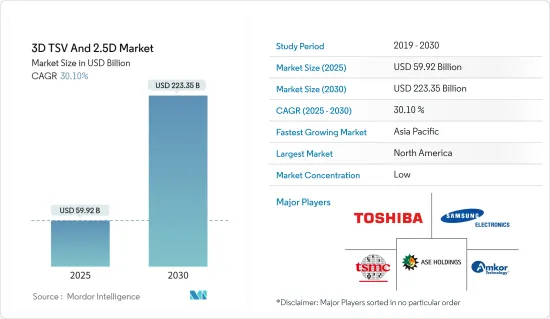
3D TSV 和 2.5D 市场规模在 2025 年预计为 599.2 亿美元,预计到 2030 年将达到 2233.5 亿美元,预测期内(2025-2030 年)的复合年增长率为 30.1%。
半导体产业的封装正在经历持续的变革。随着半导体应用的成长,CMOS 扩展放缓和价格上涨迫使该行业依赖IC封装的进步。 3D增材技术是满足AI、ML和资料中心等应用效能要求的解决方案。因此,在预测期内,对高效能运算应用的不断增长的需求主要推动了硅通孔 (TSV) 市场的发展。
关键亮点
- 3D TSV 封装技术也越来越受到重视。与目前的焊线技术相比,晶片之间的资料传输时间减少,从而提高速度并显着降低功耗。 2022年10月,台积电宣布推出开箱即用的3DFabric联盟。这是台积电开放创新平台(OIP)的介绍,该平台可协助客户克服快速成长的半导体和系统级设计挑战。它还将有助于加速下一代 HPC 和行动技术进步与台积电 3DFabric 技术的融合。
- 消费者对电子设备的需求不断增长,引发了对先进半导体设备的需求,以实现各种新功能。随着对半导体设备的需求不断增长,先进的封装技术正在提供当今数位化世界所需的外形规格和处理能力。例如,根据半导体产业协会的数据,2022年8月全球半导体产业销售额为474亿美元,总合2021年8月的473亿美元小幅成长0.1%。
- 而根据 GSM 协会的预测,到 2025 年,美国将成为全球智慧型手机普及率最高的国家(占连线的 49%)。根据美国物联网协会的数据,美国是每个家庭智慧家庭设备拥有率最高的国家,消费者拥有涵盖两到三个使用案例(能源、安全和家用电子电器)的家用电子电器产品的趋势最为明显。
- 此外,2022年9月,拜登政府宣布将投资500亿美元发展国内半导体产业,以抵销对中国的依赖,因为美国生产了零,却消费量了全球25%对国家安全至关重要的最先进晶片。总统拜登于 2022 年 8 月签署了价值 2800 亿美元的《CHIPS 法案》,以促进国内高科技製造业的发展,这是加强美国与中国竞争的一部分。预计半导体领域的如此强劲投资将为研究市场的成长提供有利机会。
- MEMS 和感测器的成长是由汽车和工业自动化等各种应用对感测器和显示器的需求快速增长所推动的。 2022年8月,MEMS製造商、全球半导体产业主要参与企业意法半导体(STMicroelectronics)宣布推出其第三代MEMS感测器,专为消费智慧工业、行动装置、医疗和零售领域设计。强大的晶片大小的运动和环境感测器使当今采用 MEMS 技术构建的智慧型手机和穿戴式装置能够实现用户友好的情境察觉功能。 ST 的最新一代 MEMS 感测器突破了输出精度和功耗的技术极限,将性能提升到了新的水平。
- 此外,製造 TSV 设备的高成本限制了市场的成长。这不仅包括设备的成本,还包括设备正常运作所需的任何配件和消耗品的成本。此外,製造 TSV 设备的严格准则和规定也会推高成本。
- 此外,全球半导体短缺促使参与企业专注于疫情后扩大生产能力。例如,中芯国际已宣布了积极的计划,将在各个城市建设自己的晶片製造厂,到2025年将产能翻倍。此外,许多亚太地方政府正在透过长期计划资助半导体产业,预计这将有助于恢復市场成长。例如,中国政府已引入约230至300亿美元资助国家积体电路投资基金2030的第二阶段。
- 此外,俄罗斯和乌克兰之间持续的衝突预计将对电子产业产生重大影响。这场衝突已经加剧了影响该行业一段时间的半导体供应链问题和晶片短缺问题。这种中断可能表现为镍、钯、铜、钛、铝和铁矿石等主要原料的价格波动,并可能导致材料短缺。这导致3D堆迭记忆体的生产受到阻碍。
3D TSV 和 2.5D 市场趋势
LED构装可望大幅成长
- LED 在产品中的使用日益增多,推动了高功率、更高密度、更低成本设备的扩张。与二维封装不同,采用硅穿孔电极(TSV) 技术的3D(3D) 封装可实现高密度垂直互连。
- TSV积体电路提供更短的连接长度,从而降低寄生电容、电感和电阻,从而实现单晶片和多功能整合的有效组合,并实现高速、低功耗互连。根据IEA预测,2025年LED在国际照明市场的渗透率预计将达到76%左右,2030年将进一步达到87.4%。
- 此外,政府采用节能 LED 的措施和法规也在推动所研究市场的发展。根据国际能源总署(IEA)的预测,到2025年,LED在照明市场的份额预计将成长75.8%。
- LED构装要求还有待提高。如果LED晶片在封装中的位置不准确,可能会直接影响整个封装设备的发光效率。如果没有对准,LED光就不会从反光杯中充分反射,进而影响LED的亮度。
- 美国能源局最近宣布将投资 6,100 万美元用于 10 个试点计划,利用最新技术将数千个家庭和企业转变为先进的节能网路。这也适用于从白炽灯或卤素灯泡转换为更节能的 LED 照明。因此,随着 LED 的扩张,预测期内美国的LED构装需求将会成长。
- 此外,市场中的各种参与企业正在研究的市场中开发新产品。 2022 年 5 月,Lumileds LLC 推出高功率 CSP(晶片级封装)LED。 LUXEON HL1Z 是一种非圆顶型单面光源,可在仅 1.4 平方毫米的小盒子中提供高发光效率(137lm/W 或更高)。
- LED构装应用的快速进步预计将在未来几年推动技术创新和消费,从而推动研究市场的成长。另一方面,高饱和度可能会限制产品的接受度,从而限制市场成长。
亚太地区可望占据主要市场占有率
- 亚太地区是该市场的一个重要的成长地区。智慧型手机普及率的不断上升使得该地区成为全球领先的行动市场之一。
- 根据GSM协会统计,智慧型手机宽频网路覆盖亚太地区96%的人口,共有12亿人使用行动网路服务。 5G 发展势头在亚洲持续,目前已有 14 个市场供应商使用 5G 服务。预计印度和越南等其他几个市场也将在未来几年内推出商业服务。到 2025 年,预计该全部区域将拥有 4 亿个 5G 连接,占总人口的 14% 以上。此外,工业4.0也是亚太地区最热门的趋势之一。物联网设备和小型化是利用 3D TSV 的工业 4.0 的主要趋势。该地区正在大力投资物联网以支援智慧城市基础设施。
- 科技的发展推动了家用电子电器、通讯、医疗设备、通讯设备和汽车的进步。中国即将推出 5G 服务,将刺激需求,尤其是对智慧型手机的需求。
- 据工信部称,中国计划在2022年安装200万个5G基地台,以发展下一代行动网路。根据工信部统计,目前,中国当地已建成142.5万个5G基地台,支撑全国5亿多5G用户,是全球最完善的网路。该地区 5G 的日益普及预计将推动对 5G 设备的需求,从而增加对 2.5D 和 3D 半导体封装的需求。
- 此外,根据中国信通院统计,5G智慧型手机出货量占国内出货量的75.9%,高于全球平均的40.7%。到2022年7月,预计5G智慧型手机将占中国行动电话整体出货量的74%。截至2022年7月,5G行动电话总出货量约在1.24亿支部左右,中国将推出121款新5G行动电话。这些趋势预计将加速该地区对 2.5D 和 3D 半导体封装解决方案的需求。
- 自动驾驶汽车和电动车的使用日益增多也增加了全部区域先进半导体的需求,进一步推动了研究市场的成长。 2022年2月,特斯拉计划在中国建造第二家电动车工厂,以满足国内和出口市场日益增长的需求。短期内,特斯拉打算将在中国的生产能力提升至至少每年100万辆,并计画在上海临港自贸区目前的展览中心附近建立第二家工厂。此外,中国政府的目标是到2025年将电动车占汽车总销量的20%,其中包括采用新能源汽车作为下一代公务车。
- 此外,对半导体製造和封装工厂的投资增加也为所研究的市场创造了有利的成长前景。例如,领先的半导体晶片製造商英特尔最近宣布将投资70亿美元在马来西亚建造先进的晶片封装工厂。同样,2022年11月,日月光(ASE)宣布投资3亿美元扩建其在马来西亚的生产基地。
3D TSV 和 2.5D 产业概览
3D TSV 和 2.5D 市场竞争激烈且多样化,拥有多种主要参与者。市场上有小型、大型和本地供应商,形成了良好的竞争。这些公司正在建立策略合作关係,以扩大市场占有率并提高盈利。此外,该市场中的公司正在收购致力于企业网路设备技术的新兴企业,以增强其产品能力。
2022 年 8 月,英特尔公布了独特的架构和封装突破,有助于基于 2.5D 和 3D 的晶片设计,开创了晶片製造技术及其重要性的非凡时代。英特尔System Foundry模式的显着特点就是增强封装。该组织计划在2030年将封装电晶体的数量从1000亿个提高到1兆个。
2022 年 3 月,Apple 采用 2.5D 方法为其最新的 M1 Ultra 设备提供动力,为未来利用小晶片的设计打开了大门。这种名为 UltraFusion 的封装架构将两个 M1 Max 晶片晶粒在硅内插器上互连,从而形成一个包含 1,140 亿个电晶体的系统单晶片 (SoC)。它利用硅基基板和内插器来支援两个具有 10,000 个低延迟互连的晶粒,并且两个晶粒之间的处理器间频宽为 2.5TB/s。它还连接到以 800GB/s 介面运行的 128GB 低延迟统一记忆体。
其他福利
- Excel 格式的市场预测 (ME) 表
- 3 个月的分析师支持
目录
第 1 章 简介
- 研究假设和市场定义
- 研究范围
第二章调查方法
第三章执行摘要
第四章 市场洞察
- 市场概况
- 产业吸引力-波特五力分析
- 供应商的议价能力
- 买家的议价能力
- 新进入者的威胁
- 替代品的威胁
- 竞争对手之间的竞争强度
- 产业价值链分析
- 宏观经济趋势对市场的影响
第五章 市场动态
- 市场驱动因素
- 高效能运算应用市场的扩大
- 资料中心和储存设备的成长
- 市场问题
- IC封装单价高
第六章 技术简介
第七章 市场区隔
- 按包装类型
- 3D堆迭内存
- 2.5D内插器
- 带有 TSV 的 CIS
- 3D SoC
- 其他封装类型(LED、MEMS 和感测器等)
- 按最终用户应用
- 消费性电子产品
- 车
- 高效能运算 (HPC) 和网络
- 其他最终用户应用程式
- 按地区
- 北美洲
- 美国
- 加拿大
- 欧洲
- 英国
- 德国
- 法国
- 义大利
- 欧洲其他地区
- 亚太地区
- 中国
- 印度
- 日本
- 澳洲
- 东南亚
- 其他亚太地区
- 其他的
- 北美洲
第八章 竞争格局
- 公司简介
- Toshiba Corp.
- Samsung Electronics Co. Ltd.
- ASE Group
- Taiwan Semiconductor Manufacturing Company Limited
- Amkor Technology, Inc.
- Pure Storage Inc.
- United Microelectronics Corp.
- STMicroelectronics NV
- Broadcom Ltd.
- Intel Corporation
- Jiangsu Changing Electronics Technology Co. Ltd.
第九章投资分析
第十章:市场的未来
The 3D TSV And 2.5D Market size is estimated at USD 59.92 billion in 2025, and is expected to reach USD 223.35 billion by 2030, at a CAGR of 30.1% during the forecast period (2025-2030).
Packaging in the semiconductor industry has noticed a continuous transformation. As the semiconductor applications are growing, the slowdown in CMOS scaling and escalating prices have forced the industry to rely on the advancement in IC packaging. 3D stacking technologies are the solution that meets the required performance of applications like AI, ML, and data centers. Therefore, the growing requirement for high-performance computing applications mainly drives the TSV (Through Silicon Via) market over the forecast period.
Key Highlights
- The 3D TSV packaging technology is also achieving traction. It reduces data transmission time between chips and the current wire bonding technology, resulting in significantly lower power consumption with faster speed. In October 2022, TSMC announced the launch of the creative 3DFabric Alliance, a considerable introduction to TSMC's Open Innovation Platform (OIP) to help customers overcome the surging hurdles of semiconductor and system-level design challenges. It will also help in gaining rapid integration of advancements for next-generation HPC and mobile technologies using TSMC's 3DFabric technologies.
- Increasing consumer demand for electronics has sparked the need for advanced semiconductor devices that enable various new capabilities. As the demands for semiconductor appliances intensify consistently, advanced packaging techniques deliver the form factor and processing power required for today's digitized world. For instance, according to the Semiconductor Industry Association, during August 2022, global semiconductor industry sales were USD 47.4 billion, a slight boost of 0.1% over the August 2021 total of USD 47.3 billion.
- In addition, according to the GSM Association, by 2025, the United States is expected to have the highest smartphone adoption globally (49% of connections). As per the United States IoT Association, it has the highest smart home device ratio per household and the most significant consumer tendency to own appliances across two or three use cases (energy, security, and appliances).
- Moreover, in September 2022, the Biden administration announced that it would invest USD 50 billion in building up the domestic semiconductor industry to counter dependency on China, as the US produces zero and consumes 25% of the world's leading-edge chips vital for its national security. President Joe Biden signed a USD 280 billion CHIPS bill in August 2022 to boost domestic high-tech manufacturing, part of his administration's push to increase US competitiveness over China. Such robust investments in the semiconductor sector would present lucrative opportunities for the growth of the studied market.
- The growth of MEMS and Sensors is attributed to the rapidly increasing demand for sensors and displays in various applications such as automotive, industrial automation, and many others. In August 2022, STMicroelectronics, a maker of MEMS and a significant player in the worldwide semiconductor industry, launched its third generation of MEMS sensors designed for consumer smart industries, mobile devices, healthcare, and retail sectors. The robust, chip-sized motion and environmental sensors power the user-friendly, context-aware features of today's smartphones, and wearables are made on MEMS technology. ST's most recent MEMS sensor generation drives technical boundaries regarding output accuracy and power consumption, elevating performance to a new level.
- Furthermore, the high costs associated with TSV device manufacturing restrict market growth. This includes not only the cost of devices but also the cost of accessories and consumables needed for their proper functioning. Moreover, the stringent guidelines and regulations governing TSV device manufacturing also add to the charges.
- Furthermore, the worldwide semiconductor shortage encouraged players to focus on expanding production capacity during a post-pandemic. For instance, the SMIC announced aggressive plans to double its production capacity by 2025 by constructing unique chip fabrication plants in different cities. Also, many Asian-Pacific local governments have funded the semiconductor industry in a long-term program, hence anticipated to regain market growth. For instance, the Chinese government introduced roughly USD 23-30 billion to pay for the second stage of its National IC Investment Fund 2030.
- Moreover, the ongoing conflict between Russia and Ukraine is expected to impact the electronics industry significantly. The conflict has already exacerbated the semiconductor supply chain issues and the chip shortage that have affected the industry for some time. The disruption may come in the form of volatile pricing for critical raw materials such as nickel, palladium, copper, titanium, aluminum, and iron ore, resulting in material shortages. This would obstruct the manufacturing of 3D Stacked Memory.
3D TSV And 2.5D Market Trends
LED Packaging Expected to Witness the Significant Growth
- The increasing use of LED in products has promoted the expansion of higher power, greater density, and lower-cost devices. Using three-dimensional (3D) packaging through silicon via (TSV) technology authorizes a high density of vertical interconnects, unlike 2D packaging.
- TSV integrated circuits reduce connection lengths; thus, smaller parasitic capacitance, inductance, and resistance are required where a combination of monolithic and multifunctional integration is done efficiently, providing high-speed, low-power interconnects. According to IEA, the penetration rate of LEDs into the international lighting market is expected to reach some 76% in 2025 and further to 87.4% in 2030.
- Further, government initiatives and rules to adopt energy-efficient LEDs drive the studied Market. According to the International Energy Agency (IEA), the growth rate of LEDs in the lighting market is anticipated to be 75.8% in 2025.
- The requirements for LED packaging could be much better. If LED chips are not positioned into the package precisely, the luminescence efficiency of the overall packaging appliance might be affected directly. Any deviation from the established position will prevent LED light from being fully reflected from the reflective cup, affecting the LED's brightness.
- The US Department of Energy recently announced investing USD 61 million in 10 pilot projects using the latest technologies to turn thousands of homes and businesses into cutting-edge, energy-efficient networks. This applies to switching out incandescent and halogen bulbs for better energy-efficient LED lighting. As a result, with the expansion in LEDs, the LED packaging need in the United States will grow in the forecasted period.
- Furthermore, various players in the market are developing new products in the studied Market. In May 2022, Lumileds LLC launched high-power CSP (chip-scale package) LED. The LUXEON HL1Z is an un-domed, single-sided emitter that delivers high luminous efficacy (137lm/W or more) from a tiny box, just 1.4mm square.
- Rapid advancements in LED package applications are projected to raise innovation and consumption in the coming years, propelling the studied market growth. On the other hand, high saturation may limit product acceptance, which, in turn, limits market growth.
Asia-Pacific is Expected to Hold the Significant Market Share
- Asia-Pacific is the significant-growing region in the Market studied. The rising smartphone adoption rates have made the region one of the major mobile markets in the world, primarily due to the increasing population evolution and urbanization.
- As per the GSM Association, smartphone broadband networks cover 96% of the population of APAC, with 1.2 billion people accessing mobile internet services. 5G momentum continues revving across the region, with commercial 5G services currently available across 14 markets. Several others, including India and Vietnam, are expected to board in the coming years. By 2025, there will be 400 million 5G connections across the region, over 14% of the population. Further, industry 4.0 is also one of Asia-Pacific's most emerging trends. IoT devices and miniaturization are important trends in Industry 4.0, utilizing 3D TSV. The region is investing heavily in IoT to support smart city infrastructure.
- Advancing technologies have contributed to the development of consumer electronics, telecom, medical devices, communication devices, and automotive. With the launch of 5G benefits in the country, the demand for smartphones, among other things, has been rising.
- According to the MIIT, China desired 2 million installed 5G base stations in 2022 to develop the country's next-generation mobile network. The Chinese mainland presently has 1.425 million installed 5G base stations that support more than 500 million 5G users nationally, making it the most comprehensive network in the world, as per MIIT. The growing implementation of 5G in the region is also expected to promote the demand for 5G-enabled devices, thereby increasing the need for 2.5D and 3D semiconductor packaging.
- Further, according to CAICT, 5G smartphone shipments are recorded for 75.9% of domestic shipments, more significant than a global average of 40.7%. By July 2022, 5G smartphones will have reached 74% of all cellphone shipments in China. The total number of 5G cell phone shipments by July 2022 was 124mm units, and China introduced 121 latest 5G mobile phone models. Such trends would accelerate the region's demand for 2.5D and 3D semiconductor packaging solutions.
- The increasing use of autonomous and electric vehicles has also increased the demand for advanced semiconductors across the region, further supporting the studied Market's growth. In February 2022, Tesla plans to build a 2nd EV facility in China to keep up with rising demand locally and in export markets. In the short term, Tesla intends to increase capacity in China to at least 1mm cars yearly, with a second plant planned around its present exhibition in Shanghai's Lingang free trade zone. In addition, the Chinese government seeks 20% of all vehicle sales to be electric by 2025, including adopting NEVs as the next generation of government vehicles.
- Moreover, the growing investments in semiconductor manufacturing and packaging plants also create a favorable growth scenario for the studied Market. For instance, Intel, a significant semiconductor chip manufacturer, recently announced a USD 7 billion investment to build an advanced chip packaging facility in Malaysia. Similarly, in November 2022, Advanced Semiconductor Engineering (ASE) announced a USD 300 million investment to expand its production site in Malaysia.
3D TSV And 2.5D Industry Overview
The 3D TSV and 2.5D market is highly competitive and consists of various significant performers as it is diversified. The existence of small, large, and local vendors in the Market creates excellent competition. These firms leverage strategic collaborative endeavors to expand their market share and increase profitability. The companies in the Market are also acquiring start-ups performing on enterprise network equipment technologies to strengthen their product capabilities.
In August 2022, Intel showcased the unique architectural and packaging breakthroughs that help 2.5D and 3D-based chip designs, ushering in a remarkable era in chipmaking technologies and their importance. Intel's system foundry model features enhanced packaging. The organization intends to improve the number of transistors on a package from 100 billion to 1 trillion by 2030.
In March 2022, Apple adopted a 2.5D approach to boost the enactment of its latest M1 Ultra device that unlocks the door to future designs utilizing chiplets. A packaging architecture called UltraFusion interconnects the die of two M1 Max chips on a silicon interposer to build a system on a chip (SoC) with 114bn transistors. This utilizes a silicon substrate and interposer that supports the two dies with 10,000 interconnects with 2.5 TB/s of low latency and inter-processor bandwidth between the die. This also connects the die to 128 GB of low-latency unified memory operating an 800 GB/s interface.
Additional Benefits:
- The market estimate (ME) sheet in Excel format
- 3 months of analyst support
TABLE OF CONTENTS
1 INTRODUCTION
- 1.1 Study Assumptions and Market Definitions
- 1.2 Scope of the Study
2 RESEARCH METHODOLOGY
3 EXECUTIVE SUMMARY
4 MARKET INSIGHTS
- 4.1 Market Overview
- 4.2 Industry Attractiveness - Porter's Five Forces Analysis
- 4.2.1 Bargaining Power of Suppliers
- 4.2.2 Bargaining Power of Buyers
- 4.2.3 Threat of New Entrants
- 4.2.4 Threat of Substitute Products
- 4.2.5 Intensity of Competitive Rivalry
- 4.3 Industry Value Chain Analysis
- 4.4 Impact of Macroeconomic Trends on the Market
5 MARKET DYNAMICS
- 5.1 Market Drivers
- 5.1.1 Expanding Market for High Performance Computing Application
- 5.1.2 Expanding Scope of Data Centers and Memory Devices
- 5.2 Market Challenges
- 5.2.1 High Unit Cost of IC Packages
6 TECHNOLOGICAL SNAPSHOT
7 MARKET SEGMENTATION
- 7.1 By Packaging Type
- 7.1.1 3D Stacked Memory
- 7.1.2 2.5D Interposer
- 7.1.3 CIS with TSV
- 7.1.4 3D SoC
- 7.1.5 Other Packaging Types ( LED, MEMS & Sensors, etc.)
- 7.2 By End User Application
- 7.2.1 Consumer Electronics
- 7.2.2 Automotive
- 7.2.3 High Performance Computing (HPC) and Networking
- 7.2.4 Other End User Applications
- 7.3 By Geography
- 7.3.1 North America
- 7.3.1.1 U.S.
- 7.3.1.2 Canada
- 7.3.2 Europe
- 7.3.2.1 United Kingdom
- 7.3.2.2 Germany
- 7.3.2.3 France
- 7.3.2.4 Italy
- 7.3.2.5 Rest of Europe
- 7.3.3 Asia-Pacific
- 7.3.3.1 China
- 7.3.3.2 India
- 7.3.3.3 Japan
- 7.3.3.4 Australia
- 7.3.3.5 South East Asia
- 7.3.3.6 Rest of Asia-Pacific
- 7.3.4 Rest of the World
- 7.3.1 North America
8 COMPETITIVE LANDSCAPE
- 8.1 Company Profiles
- 8.1.1 Toshiba Corp.
- 8.1.2 Samsung Electronics Co. Ltd.
- 8.1.3 ASE Group
- 8.1.4 Taiwan Semiconductor Manufacturing Company Limited
- 8.1.5 Amkor Technology, Inc.
- 8.1.6 Pure Storage Inc.
- 8.1.7 United Microelectronics Corp.
- 8.1.8 STMicroelectronics NV
- 8.1.9 Broadcom Ltd.
- 8.1.10 Intel Corporation
- 8.1.11 Jiangsu Changing Electronics Technology Co. Ltd.
9 INVESTMENT ANALYSIS
10 FUTURE OF THE MARKET
 3D积体电路(3D IC)在半导体产业转型的技术进步
 2026年三维(3D)积体电路(IC)全球市场报告
 3D IC市场规模、份额和成长分析(按组件、应用、最终用户和地区划分)—产业预测,2026-2033年全球3D TSV元件市场-2025-2030年预测
 3D TSV 市场(按 TSV材料类型、晶圆尺寸、封装类型、应用和最终用户行业)- 全球预测,2025 年至 2032 年
 3D TSV 与 2.5D 全球市场3D积体电路市场 - 2025年至2030年预测
 3D IC 市场按最终用途领域、基板类型、製造流程、产品类型和地区划分 - 市场规模、份额、展望、机会分析,2020-2027 年
 3D 积体电路市场分析和预测至 2033 年:按类型、产品、服务、技术、应用、材料类型、流程、部署、最终用户和功能
 2025-2033 年按类型、组件(硅通孔、玻璃通孔、硅中介层)、应用、最终用户和地区分類的 3D IC 市场