


 |
市场调查报告书
商品编码
1687872
面板级封装:市场占有率分析、产业趋势与统计资料、成长预测(2025-2030 年)Panel Level Packaging - Market Share Analysis, Industry Trends & Statistics, Growth Forecasts (2025 - 2030) |
||||||
※ 本网页内容可能与最新版本有所差异。详细情况请与我们联繫。
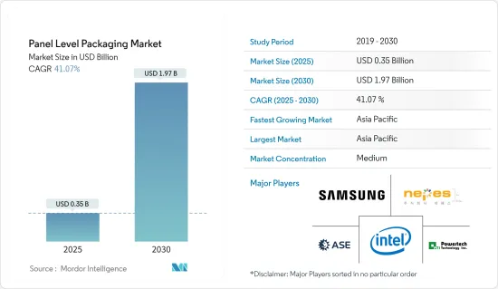
面板级封装市场规模预计在 2025 年为 3.5 亿美元,预计到 2030 年将达到 19.7 亿美元,预测期内(2025-2030 年)的复合年增长率为 41.07%。
半导体产业正在经历快速成长,半导体成为所有现代技术的基本组成部分。该领域的进步和创新直接影响所有下游技术,推动市场研究的需求。
关键亮点
- 随着半导体产业重要性的不断增长,对增强型封装解决方案的需求也日益增长,从而推动了新型半导体封装技术的发展。
- 面板级封装(PLP)是一项最近备受关注的技术。 PLP是指以面板尺寸加工的半导体封装。在面板级封装中,组装过程包括面板级的晶片贴装、重新布线、成型和凸点製造。
- 由于采用面板平行格式处理大量封装,因此与圆形晶圆形式相比,这种封装类型有利于实现更好的面积利用率(面板/晶圆尺寸与封装尺寸的比率)。因此,降低包装成本是市场成长的主要驱动力之一。 PLP 对环境的影响也很小,因为它产生的废弃物较少,留下的碳足迹也较少。
- 面板级封装(PLP)市场并不缺乏挑战。该技术的巨大成本及其实施的复杂性可能会阻碍其广泛接受。封装製程有两种:先塑封 (mold 领先)和先RDL (RDL 领先)。然而,某些类型的封装可能会导致晶片移位问题。晶片移位被认为是最大的问题之一,因为它会降低产量比率并对产量比率负面影响。这导致对包装过程的控制需求不断增加,增加了复杂性并抑制了市场成长。
- 在新冠疫情 (COVID-19) 之后,我们预计由于成本效益以及封装尺寸从晶圆到大面板格式的扩展,面板级封装将受到更多关注。并行生产的封装数量不断增加也是支持市场成长的一大优势。 PLP 可能会采用其其他技术部门的製程、材料和设备。印刷电路基板(PCB)、液晶显示器(LCD)、太阳能设备等都是以面板尺寸製造的,为扇出面板级封装提供了一种新方法。
面板级封装市场趋势
市场区隔以消费性电子领域为主
- 智慧型手机、穿戴式装置、平板装置等家用电子电器产品正变得越来越薄、越来越小。 PLP 满足了对更小、更轻的组件的需求,使製造商能够提高组件密度并更有效地利用空间。对于这些设备,PLP 提供的减少的占用空间对于实现时尚的设计和最大限度地利用可用空间至关重要。
- 家用电子电器产业与力求产品差异化的製造商竞争。 PLP 可实现家用电子电器更时尚的设计、更强大的功能和更佳的效能,从而为您带来市场优势。为了维持市场地位,製造商正在使用 PLP 来满足消费者需求并推出创新产品。
- 近年来,5G和物联网的日益普及为市场带来了巨大的成长机会。例如,根据5G Americas的预测,全球5G用户数将在2024年达到28亿,2027年达到59亿。
- 随着对 5G 的投资不断增长,对支援 5G 的智慧型手机的需求也在同步增长。根据 CyberMedia Research 的报告,自 2020 年首次推出以来,5G 智慧型手机销量成长了 13 倍,到 2023 年底,5G 智慧型手机出货量预计将以每年 70% 的速度成长。 5G 智慧型手机市场占有率在 2020 年仅为 4%,预计到 2023 年将达到 45%。
- 同样,由于物联网 (IoT) 的日益普及,近年来连接设备的数量也迅速增长,物联网是一种使事物和人们能够使用互联网和 IP通讯协定进行通讯的技术。例如,根据思科预测,到2023年,连网设备数量将达到293亿台。物联网用例的大幅扩展预计将成为市场成长的主要驱动力。
中国可望引领市场
- 中国是最大的半导体消费国,这主要得益于其国内电子产品市场的规模。中国是世界上最大的家用电子电器生产国和出口国,许多全球供应商已在该国设立工厂,以利用其低廉的劳动力成本。
- 电子製造业近年来也稳定扩张。根据工业信部报告,2023年电子资讯製造业主要企业工业增加价值年平均成长3.4%。根据工信部统计,主要产品中,行动电话产量15.7亿部,与前一年同期比较去年成长6.9%。其中,智慧型手机产量11.4亿部,与前一年同期比较增1.9%。近年来,政府采取了多项措施来促进电子产业的发展。
- 中国在5G部署方面也处于世界领先地位。据工业和资讯化部称,中国的目标是到 2023 年 2 月拥有 5.9201 亿 5G 用户。预计到 2025 年,这一数字将超过 10 亿。中国正在进行基础设施建设,以扩大 5G 在全国的覆盖范围。
- 例如,截至2023年10月,中国拥有约322万个5G基地台,占行动基地台总数的28.1%。
- 随着5G在国内的推广与推进,5G设备的普及率也不断提高。例如,根据中国资讯通讯研究院(CAICT)的预测,2023年中国5G智慧型手机出货量将达到2.4亿部,与前一年同期比较增长约11.9%,而整体智慧型手机出货量市场将比与前一年同期比较增长约1.1%。由于先进的封装技术可以帮助满足 5G 晶片的许多性能要求,预计这一趋势将有利于该国研究市场的成长。
- 此外,中国在汽车生产和消费方面均处于领先地位,预计这将有利于该国的市场成长。对更清洁、更安全的汽车的需求不断增长是该国汽车行业的主要趋势之一,推动了市场的成长。自动驾驶汽车、电气化、座舱丰富化、连接性和软体定义以及区域架构等市场大趋势也在支持汽车领域的市场成长。
面板级封装产业概览
面板级封装市场处于半固体状态,主要参与者包括三星电子、英特尔公司、Nepes 公司、ASE 集团和 Powertech Technology Inc.。市场参与企业正在采取联盟和收购等策略来加强其产品供应并获得可持续的竞争优势。
- 2023年12月-NEPES开发用于边缘运算的智慧半导体「METIS」。 Metis 采用了 Nepes 最先进的 2.5D 和 3D 封装平台 nePAC™ 的 cx-BGA(球栅阵列)。 nePACTM是基于扇出型和覆晶键合技术实现多层、精细RDL布线的下一代尖端封装技术。适用于人工智慧半导体等高整合、高性能晶片。
- 2023年6月,日月光科技控股子公司USI在波兰设立工厂。此举反映出欧洲客户对该公司产品的需求不断成长。此次扩张将使 USI 能够在波兰生产更多产品,以满足客户需求并跟上市场成长。
其他福利
- Excel 格式的市场预测 (ME) 表
- 3个月的分析师支持
目录
第一章 引言
- 研究假设和市场定义
- 研究范围
第二章调查方法
第三章执行摘要
第四章 市场洞察
- 市场概览
- 产业吸引力-波特五力分析
- 供应商的议价能力
- 买家的议价能力
- 新进入者的威胁
- 替代品的威胁
- 竞争对手之间的竞争强度
- 产业价值链/供应链分析
- 评估宏观经济因素对市场的影响
第五章市场动态
- 市场驱动因素
- 降低包装过程的成本
- 对紧凑、高功能电子设备的需求不断增长
- 增加研发投入
- 市场限制
- 包装工艺日益复杂
第六章市场区隔
- 产业应用
- 消费性电子产品
- 车
- 通讯
- 其他工业应用
- 按地区
- 美国
- 中国
- 韩国
- 台湾
- 日本
- 欧洲
- 其他的
第七章竞争格局
- 公司简介
- Samsung Electronics Co. Ltd
- Intel Corporation
- Nepes Corporation
- ASE Group
- Powertech Technology Inc.
- Fraunhofer Institute for Reliability and Micro integration IZM
- Unimicron Technology Corporation
- DECA Technologies Inc.
- JCET/STATSChipPAC
第八章投资分析
第九章:市场的未来
The Panel Level Packaging Market size is estimated at USD 0.35 billion in 2025, and is expected to reach USD 1.97 billion by 2030, at a CAGR of 41.07% during the forecast period (2025-2030).
The semiconductor industry is witnessing rapid growth, with semiconductors emerging as the basic building blocks of all modern technology. The advancements and innovations in this field directly impact all downstream technologies and drive the need for the market studied.
Key Highlights
- With the importance of the semiconductor industry growing, the demand for enhanced packaging solutions is also increasing, leading to the development of new semiconductor packaging techniques.
- Panel-level packaging (PLP) is a technology that has gained prominence recently. PLP refers to semiconductor packaging processed on a panel size. In panel-level packaging, the assembly process includes the fabrication of die attach, redistribution lines, molding, and bumping at the panel level.
- As more packages may be processed in panel and parallel formats, this type of packaging facilitates a much better area utilization (ratio between panel/wafer size and package size) compared to round wafer shapes. Hence, a lower packaging cost is among the primary drivers for the market's growth. PLP has a lower environmental impact due to a lower waste generation and carbon footprint.
- The panel-level packaging (PLP) market also encounters certain challenges. The substantial expenses linked to the technology and the intricate nature of its implementation might impede its extensive acceptance. The packaging process involves both types, mold first and RDL first. However, the type of packaging involves problems in die shift. Shifting the die is considered one of the biggest issues as it may cause lesser yield or negatively influence the yields. This increases the need for more control over the packaging process and adds complexity, restraining the market's growth.
- In the post-COVID-19 period, the focus on panel-level packaging is anticipated to increase due to the cost benefits and the expansion of the packaging size from wafers to larger panel formats. Increasing the number of packages manufactured in parallel is another major advantage supporting the market's growth. PLP may adopt processes, materials, and equipment from other technology areas. Printed circuit boards (PCB), liquid crystal displays (LCD), or solar equipment are manufactured on panel sizes and offer new approaches for fan-out panel-level packaging.
Panel Level Packaging Market Trends
Consumer Electronics Segment to Hold Major Market Share
- Consumer electronics such as smartphones, wearables, and tablets are becoming increasingly thin and compact. To meet the needs of miniaturization and light form factors, PLP allows manufacturers to achieve greater component density and more efficient use of space. For these devices, the reduced footprint caused by PLP is essential as it will enable sleek designs and maximize their utilization of available space.
- The consumer electronics industry competes with manufacturers who strive to differentiate products. By enabling sleek designs, increased functionality, and improved performance for consumer electronics devices, PLP provides an advantage to the market. To maintain their position in the market, manufacturers take advantage of PLP to meet consumer demands and introduce innovative products.
- The increasing penetration of 5G and IoT in recent years presents significant growth opportunities for the market. For instance, as per 5G Americas, the 5G subscriptions worldwide are estimated to reach 2.8 billion in 2024 and 5.9 billion by 2027.
- With the rising investments in 5G, the demand for 5G-enabled smartphones is also increasing parallelly. According to a report from Cybermedia Research, by the end of 2023, after recording a 13 times increase in 5G smartphone sales since its first introduction in 2020, shipments of 5G smartphones increased by 70% yearly. From only 4% in 2020, 5G smartphones were projected to capture a possible 45% market share in 2023.
- Similarly, owing to the rising adoption of the Internet of Things (IoT), the technology that enables communications between things and people using the Internet and IP-enabled protocols, the number of connected devices has been increasing rapidly in recent years. For instance, as per Cisco, there would be 29.3 billion networked devices in 2023. The massive expansion in IoT use cases will provide a significant impetus to market growth.
China is Expected to Lead the Market
- China is the largest semiconductor consumer, primarily due to the size of the domestic electronics market. The country is the world's largest producer and exporter of consumer electronics, as a significantly more significant number of global vendors have established their facilities to leverage the benefits of cheap labor costs.
- The electronics manufacturing industry has also recently continued to maintain steady expansion. As per a report by the Ministry of Industry and Information Technology via China Daily, in 2023, the industrial added value of major companies in the electronic information manufacturing sector grew by 3.4% yearly. According to the ministry, among significant products, the output of mobile phones increased by 6.9% Y-o-Y to 1.57 billion units, within which the number of smartphones increased by 1.9% Y-o-Y to 1.14 billion units. Several initiatives have been taken in recent years to boost the electronics industry's growth.
- China also leads in 5G adoption globally. According to the Ministry of Industry and Information Technology (MIIT), China aims to have 592.01 million 5G users as of February 2023. This number is anticipated to surpass 1 billion mark by 2025. A combined effort is being made to develop the supporting infrastructure to expand the footprint of 5G across the country.
- For instance, as of October 2023, China had about 3.22 million 5G base stations, constituting 28.1% of its entire mobile base station.
- The growing implementation of 5G in the country has also increased the uptake of 5G-enabled devices. For instance, according to the China Academy of Information and Communications Technology (CAICT), in 2023, 5G smartphone shipments in the country grew by about 11.9% Y-o-Y to 240 million units, while the overall smartphone shipments market grew by about 1.1%, compared to the previous year. As advanced packaging technologies may help resolve many of the 5G chip performance requirements, such trends are anticipated to favor the studied market's growth in the country.
- China is also a leading automotive market in production and consumption, which is anticipated to favor the market's growth in the country. The rising demand for cleaner and safer vehicles is among the major trends in the country's automotive industry, which supports the studied market's growth. Industry megatrends, including autonomous vehicles, electrification, enriched cabins, connectivity and software definition, and zonal architecture, also support the market's growth in the automotive segment.
Panel Level Packaging Industry Overview
The panel level packaging market is semi-consolidated with the presence of major players like Samsung Electronics Co. Ltd, Intel Corporation, Nepes Corporation, ASE Group, and Powertech Technology Inc. Players in the market are adopting strategies such as partnerships and acquisitions to enhance their product offerings and gain sustainable competitive advantage.
- December 2023 - NEPES developed 'METIS,' an intelligent semiconductor for edge computing. Metis applied cx-BGA (Ball Grid Array) of nePACTM, Nepes' cutting-edge 2.5D & 3D package platform. nePACTM is a next-generation cutting-edge package technology that implements multi-layer and fine RDL wiring based on fan-out technology and flip-chip bonding technology. It is suitable for highly integrated, high-performance chips such as artificial intelligence semiconductors.
- June 2023 - USI, a subsidiary of ASE Technology Holding Co. Ltd, inaugurated another factory in Poland. This move reflects the growing need for the company's products from European customers. By expanding, USI may make more goods in Poland, meet customer needs, and keep up with market growth.
Additional Benefits:
- The market estimate (ME) sheet in Excel format
- 3 months of analyst support
TABLE OF CONTENTS
1 INTRODUCTION
- 1.1 Study Assumptions and Market Definition
- 1.2 Scope of the Study
2 RESEARCH METHODOLOGY
3 EXECUTIVE SUMMARY
4 MARKET INSIGHTS
- 4.1 Market Overview
- 4.2 Industry Attractiveness - Porter's Five Forces Analysis
- 4.2.1 Bargaining Power of Suppliers
- 4.2.2 Bargaining Power of Buyers
- 4.2.3 Threat of New Entrants
- 4.2.4 Threat of Substitute Products
- 4.2.5 Intensity of Competitive Rivalry
- 4.3 Industry Value Chain/Supply Chain Analysis
- 4.4 Assessment of Impact of Macroeconomic Factors on the Market
5 MARKET DYNAMICS
- 5.1 Market Drivers
- 5.1.1 Reduced Cost of Packaging Process
- 5.1.2 Increasing Demand for Compact and High Functionality Electronic Devices
- 5.1.3 Increased Investment on Research and Development Activities
- 5.2 Market Restraints
- 5.2.1 Complexity in Packaging Process
6 MARKET SEGMENTATION
- 6.1 By Industry Application
- 6.1.1 Consumer Electronics
- 6.1.2 Automotive
- 6.1.3 Telecommunication
- 6.1.4 Other Industry Applications
- 6.2 By Geography
- 6.2.1 United States
- 6.2.2 China
- 6.2.3 Korea
- 6.2.4 Taiwan
- 6.2.5 Japan
- 6.2.6 Europe
- 6.2.7 Rest of the World
7 COMPETITIVE LANDSCAPE
- 7.1 Company Profiles
- 7.1.1 Samsung Electronics Co. Ltd
- 7.1.2 Intel Corporation
- 7.1.3 Nepes Corporation
- 7.1.4 ASE Group
- 7.1.5 Powertech Technology Inc.
- 7.1.6 Fraunhofer Institute for Reliability and Micro integration IZM
- 7.1.7 Unimicron Technology Corporation
- 7.1.8 DECA Technologies Inc.
- 7.1.9 JCET/ STATSChipPAC

