


 |
市场调查报告书
商品编码
1911415
2.5D 和 3D 半导体封装:市场占有率分析、产业趋势和统计数据、成长预测(2026-2031 年)2.5D And 3D Semiconductor Packaging - Market Share Analysis, Industry Trends & Statistics, Growth Forecasts (2026 - 2031) |
||||||
※ 本网页内容可能与最新版本有所差异。详细情况请与我们联繫。
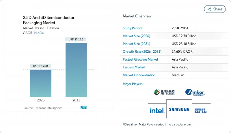
预计 2.5D 和 3D 半导体封装市场将从 2025 年的 111.2 亿美元成长到 2026 年的 127.4 亿美元,到 2031 年将达到 251.8 亿美元,2026 年至 2031 年的复合成长率为 14.6%。
在每秒Terabyte级频宽需求的AI训练丛集、汽车感测器融合平台以及空间受限的行动装置的推动下,整个生态系统正在投资于中介层产能、晶片标准和高效散热基板,以满足不断增长的需求。代工厂正在推进内部封装以确保利润率和蓝图控制,而OSAT(外包组装和测试)公司则专注于为汽车和光电应用场景提供专用组装。美国、欧洲和亚洲的政府补贴正在支持地域多角化,但硅中介层短缺和散热限制制约了短期成长空间。随着玻璃芯基板、混合键合和共封装光学元件的日益普及,未来十年,封装创新而非晶体管密度将决定係统性能。
全球2.5D及3D半导体封装市场趋势及洞察
AI/ML工作负载需要超高的记忆体频宽
拥有超过兆个参数的超大规模学习模型正使传统的DDR介面达到饱和,促使GPU厂商推广逻辑封装,从而实现每个插槽3TB/s的频宽。穿透硅通孔(TSV)缩短了互连长度,降低了延迟,并支援相邻记忆体操作,与分立式布局相比,系统电力消耗降低了15%。 CoWoS和Foveros平台将记忆体和晶粒放置在共用的中介层上。这种拓朴结构也有利于边缘推理设备,因为外形尺寸的限制使得它们无法采用分立式DIMM。三星和SK海力士的记忆体处理原型进一步模糊了逻辑和储存之间的界限,证实了2.5D和3D半导体封装市场是消除效能瓶颈的关键。资料中心营运商现在将机架能源效率指标与封装记忆体频宽直接挂钩,将封装决策转化为超大规模扩展的资本支出槓桿。
智慧型手机和穿戴式装置的微型化
高阶智慧型手机将超过 50 种功能整合到系统级封装)模组中,从而减少了 40% 的基板面积。扇出型晶圆层次电子构装将 Z 轴高度降低至 0.5 毫米以下。智慧型手錶正在追求更高的密度,需要在小于 100 平方毫米的封装内异构整合无线电、感测器和电源管理等功能。用于下一代穿戴式装置的可拉伸电子元件对机械应变提出了更高的要求,而有机基板无法满足这项要求,这推动了抗翘曲的 RDL 优先扇出製程的应用。穿戴式音讯设备和医疗设备日益普及,使得生物相容性封装和防潮层成为必需,从而扩大了 2.5D 和 3D 半导体封装在消费健康领域的市场份额。封装级电磁干扰 (EMI) 屏蔽曾经是可选的,但现在已成为口袋大小设备中毫米波通讯和超宽频测距的必备功能。
扩大对TSV/中介层製造设备的资本投资
专用CoWoS生产线的成本是标准组装的3到4倍,每条生产线的总投资额高达100亿美元。折旧免税额期延长至10年,迫使OSAT製造商承担高昂的固定成本,从而削弱了其价格竞争力。设备供应商的垄断导致前置作业时间超过18个月,增加了供应链风险。小规模的组装製造商无法资金筹措,因此正在退出高端2.5D和3D半导体封装市场,并将资源集中到上游代工厂。
细分市场分析
到2025年,3D TSV解决方案将占总收入的43.72%,维持14.85%的复合年增长率,使其在2.5D和3D半导体封装市场份额竞争中处于领先地位。三星的HBM3E堆迭每个装置可提供1.15TB/s的频宽,与平面布局相比,尺寸缩小了60%,基板电源轨减少了30%。
对人工智慧处理能力日益增长的需求推动了混合键合技术的发展,该技术无需微凸点,并将互连间距缩小至10µm以下。台积电的SoIC样品显示互连密度提高了10倍,在高产量比率下几乎可以媲美单晶片的效能。扇出晶圆层次电子构装在行动电话领域仍然至关重要,在该领域,薄化比TSV更为重要;而基于中介层的2.5D桥接技术正逐渐成为晶片级CPU的主流。在预测期内,玻璃芯和背面馈电TSV技术的应用正在模糊不同封装类型之间的界限,使混合模式封装成为事实上的高端配置,并扩大2.5D和3D半导体封装市场的整体规模。
区域分析
到2025年,亚太地区将占总营收的60.05%,主要得益于台湾的CoWoS生产线和马来西亚在全球后端生产中13%的份额。到2031年,越南和泰国为提升基板和测试产能而推出的激励措施将推动亚太地区实现15.14%的复合年增长率。
北美地区借助 CHIPS 法案拨款加速发展:英特尔位于俄亥俄州的工厂和安姆科投资 20 亿美元的亚利桑那州工厂将共同将区域处理能力提高 20%;国防封装法规将把安全工作负载转移到国内;SK 海力士计划在堪萨斯州建设的工厂将扩大 HBM组装,使其更靠近重要的云数据中心客户。
欧洲正着力发展汽车和工业可靠性领域,德国的「硅谷萨克森」(Silicon Saxony)和荷兰的光子丛集( 光电 Cluster)都获得了欧洲地平线基金的支持。儘管欧盟的市场份额落后于亚洲,但其在高可靠性领域的比例正在不断提高,从而推动了该地区2.5D和3D半导体封装市场的规模增长。虽然南美、中东和非洲等新兴地区仍在进口成品封装装置,但它们正在吸引投资以实现最终测试的本地化,这反映出全球集中供应链风险的逐步分散。
其他福利:
- Excel格式的市场预测(ME)表
- 3个月的分析师支持
目录
第一章 引言
- 研究假设和市场定义
- 调查范围
第二章调查方法
第三章执行摘要
第四章 市场情势
- 市场概览
- 市场驱动因素
- AI/ML工作负载需要超高的记忆体频宽
- 智慧型手机和穿戴式装置的微型化
- 推动汽车高阶驾驶辅助系统的电气化
- 玻璃芯基板向大量生产测试阶段过渡
- 美国国防部强制要求国内3D-IC OSAT厂商使用安全晶片
- 晶片组设计的快速普及
- 市场限制
- TSV/中介层工厂资本支出增加
- 测试设计复杂性与产量比率损耗
- 全球硅锭短缺,无法满足中介层需求
- 温度控管和可靠性限制
- 产业价值链分析
- 监管环境
- 技术展望
- 波特五力分析
- 供应商的议价能力
- 买方的议价能力
- 新进入者的威胁
- 替代品的威胁
- 竞争对手之间的竞争
第五章 市场规模与成长预测
- 透过包装技术
- 2.5D 中介层/光纤封装
- 3D堆迭(TSV/混合键结)
- 晶圆级CSP
- 按最终用户行业划分
- 家用电子电器
- 资料中心和高效能运算
- 通讯和电信
- 汽车和ADAS
- 医疗设备
- 工业和物联网
- 其他终端用户产业
- 透过使用
- 高效能逻辑晶片(CPU、GPU、AI加速器、ASIC、FPGA)
- 记忆体(HBM、DRAM 堆迭、3D NAND)
- 射频和光电
- 混合讯号和感测器整合(ADC/DAC混合讯号积体电路、MEMS感测器、感测器集线器封装)
- 按地区
- 北美洲
- 美国
- 加拿大
- 墨西哥
- 欧洲
- 德国
- 法国
- 英国
- 义大利
- 其他欧洲地区
- 亚太地区
- 中国
- 日本
- 韩国
- 印度
- 亚太其他地区
- 南美洲
- 巴西
- 阿根廷
- 南美洲其他地区
- 中东
- 以色列
- 沙乌地阿拉伯
- 阿拉伯聯合大公国
- 其他中东地区
- 非洲
- 南非
- 埃及
- 其他非洲地区
- 北美洲
第六章 竞争情势
- 市场集中度
- 策略趋势
- 供应商定位分析
- 公司简介
- Advanced Semiconductor Engineering Inc.
- Amkor Technology Inc.
- Taiwan Semiconductor Manufacturing Company Limited
- Samsung Electronics Co., Ltd.
- Intel Corporation
- Siliconware Precision Industries Co., Ltd.
- Powertech Technology Inc.
- Jiangsu Changjiang Electronics Technology Co., Ltd.
- GlobalFoundries Inc.
- United Microelectronics Corporation
- Tezzaron Semiconductor Corporation
- STATS ChipPAC Pte. Ltd.
- TongFu Microelectronics Co., Ltd.
- Hana Micron Inc.
- Kulicke and Soffa Industries Inc.
第七章 市场机会与未来展望
The 2.5D and 3D semiconductor packaging market is expected to grow from USD 11.12 billion in 2025 to USD 12.74 billion in 2026 and is forecast to reach USD 25.18 billion by 2031 at 14.6% CAGR over 2026-2031.
Driven by AI training clusters that demand terabytes-per-second bandwidth, automotive sensor fusion platforms, and space-constrained mobile devices, the ecosystem is investing in interposer capacity, chiplet standards, and thermally efficient substrates to keep pace. Foundries have moved packaging in-house to secure margins and roadmap control, while OSATs double down on specialty assembly for automotive and photonics use cases. Government subsidies in the United States, Europe, and Asia support regional diversification, yet silicon interposer shortages and cooling limits temper near-term upside. As glass-core substrates, hybrid bonding, and co-packaged optics move toward mass adoption, packaging innovation-not transistor density-will define the next decade of system performance.
Global 2.5D And 3D Semiconductor Packaging Market Trends and Insights
AI/ML Workloads Demanding Ultra-High Memory Bandwidth
Hyperscale training models that now exceed 1 trillion parameters saturate traditional DDR interfaces, prompting GPU vendors to co-package logic with HBM3 stacks delivering 3 TB/s bandwidth-per-socket . Through-silicon vias shorten trace lengths and cut latency, enabling near-memory compute that lowers system power budgets by 15% versus discrete layouts. CoWoS and Foveros platforms position memory and accelerator dies on a shared interposer, a topology that also benefits edge inference devices where form factors prohibit discrete DIMMs. Processing-in-memory prototypes from Samsung and SK Hynix further blur boundaries between logic and storage, reinforcing the 2.5D and 3D semiconductor packaging market as a performance bottleneck eliminator. Data-center operators now tie rack energy efficiency metrics directly to packaged memory bandwidth, converting packaging decisions into capital-expense levers for hyperscale expansions.
Smartphone and Wearable Miniaturization
Premium smartphones integrate more than 50 functions inside system-in-package modules, shrinking board footprint by 40% and cutting z-height below 0.5 mm through fan-out wafer-level packaging . Smartwatches push density further, demanding heterogeneous integration of radios, sensors, and power management in packages under 100 mm2. Stretchable electronics for next-gen wearables add mechanical-strain constraints that organic substrates cannot meet, spurring adoption of warpage-resistant RDL-first fan-out processes. Biocompatible encapsulants and moisture barriers become mandatory as hearables and medical wearables proliferate, enlarging the 2.5D and 3D semiconductor packaging market addressable share within consumer health. Package-level EMI shielding, once optional, is now table stakes for millimeter-wave connectivity and ultra-wideband ranging inside pocket-sized devices.
Escalating CapEx for TSV/Interposer Fabs
Individual CoWoS lines cost 3-4 times standard assembly capacity and push total investment toward USD 10 billion per site . Depreciation periods elongate to 10 years, locking OSATs into high fixed costs that erode price agility. Equipment vendor oligopolies raise tool lead-times beyond 18 months, heightening supply-chain risk. Smaller assemblers, unable to finance TSV etch modules or hybrid-bond aligners, exit the high-end 2.5D and 3D semiconductor packaging market, concentrating power upstream at foundries.
Other drivers and restraints analyzed in the detailed report include:
- Automotive ADAS Electrification Push
- Glass-Core Substrates Entering Volume Trials
- Design-for-Test Complexity and Yield Loss
For complete list of drivers and restraints, kindly check the Table Of Contents.
Segment Analysis
3D TSV solutions captured 43.72% of 2025 revenue, and their 14.85% CAGR keeps them at the forefront of the 2.5D and 3D semiconductor packaging market share race. Samsung's HBM3E stacks supply 1.15 TB/s bandwidth per device, shrinking footprint 60% and cutting board power rails by 30% over planar layouts .
Demand for AI throughput encourages hybrid bonding that eliminates micro-bumps and pushes interconnect pitch below 10 µm. TSMC SoIC samples show 10X interconnect density gains that nearly equal monolithic reticle performance at higher yields. Fan-out wafer-level packaging stays relevant in handsets where thinness outranks TSV, while interposer-based 2.5D bridges dominate chiplet CPUs. Over the forecast, glass-core adoption and backside-power TSVs will blur categorical lines, establishing mixed-mode packages as the de facto high-end configuration, enlarging the overall 2.5D and 3D semiconductor packaging market size.
The 2. 5D and 3D Semiconductor Packaging Market Report is Segmented by Packaging Technology (2. 5D Interposer/FO-SoW, 3D Stacked TSV/Hybrid Bond, and More), End-User Industry (Consumer Electronics, Data Centre and HPC, Communications and Telecom, and More), Application (High-Performance Logic, Memory, RF and Photonics, Mixed-Signal and Sensor Integration), and Geography. The Market Forecasts are Provided in Terms of Value (USD).
Geography Analysis
Asia Pacific commanded 60.05% of 2025 revenue, driven by Taiwan's CoWoS lines and Malaysia's 13% share of global back-end output . Ongoing 15.14% CAGR through 2031 arises from Vietnamese and Thai incentives that add substrate and test capacity.
North America accelerates on the back of CHIPS Act subsidies: Intel's Ohio complex and Amkor's USD 2 billion Arizona plant together raise local throughput by 20% . Defense packaging mandates concentrate secure workloads stateside, and SK Hynix's planned Kansas facility expands HBM-logic assembly near key cloud data-center customers.
Europe focuses on automotive and industrial reliability, with Germany's Silicon Saxony and the Netherlands' photonics clusters receiving Horizon Europe funds. While share lags Asia, EU content rises in high-reliability sectors, lifting the regional 2.5D and 3D semiconductor packaging market size. Emerging regions, South America, the Middle East, and Africa, import fully packaged devices but court investment to localize final test, reflecting a gradual de-risking of globally concentrated supply chains.
- Advanced Semiconductor Engineering Inc.
- Amkor Technology Inc.
- Taiwan Semiconductor Manufacturing Company Limited
- Samsung Electronics Co., Ltd.
- Intel Corporation
- Siliconware Precision Industries Co., Ltd.
- Powertech Technology Inc.
- Jiangsu Changjiang Electronics Technology Co., Ltd.
- GlobalFoundries Inc.
- United Microelectronics Corporation
- Tezzaron Semiconductor Corporation
- STATS ChipPAC Pte. Ltd.
- TongFu Microelectronics Co., Ltd.
- Hana Micron Inc.
- Kulicke and Soffa Industries Inc.
Additional Benefits:
- The market estimate (ME) sheet in Excel format
- 3 months of analyst support
TABLE OF CONTENTS
1 INTRODUCTION
- 1.1 Study Assumptions and Market Definition
- 1.2 Scope of the Study
2 RESEARCH METHODOLOGY
3 EXECUTIVE SUMMARY
4 MARKET LANDSCAPE
- 4.1 Market Overview
- 4.2 Market Drivers
- 4.2.1 AI/ML workloads demanding ultra-high memory bandwidth
- 4.2.2 Smartphone and wearable miniaturisation
- 4.2.3 Automotive ADAS electrification push
- 4.2.4 Glass-core substrates entering volume trials
- 4.2.5 U.S. DoD secure-chip mandates for on-shore 3D-IC OSATs
- 4.2.6 Rapid Uptake of Chiplet Designes
- 4.3 Market Restraints
- 4.3.1 Escalating CapEx for TSV/interposer fabs
- 4.3.2 Design-for-test complexity and yield loss
- 4.3.3 Global interposer silicon-ingot shortage issue
- 4.3.4 Thermal-management and reliability limits
- 4.4 Industry Value-Chain Analysis
- 4.5 Regulatory Landscape
- 4.6 Technological Outlook
- 4.7 Porters Five Forces Analysis
- 4.7.1 Bargaining Power of Suppliers
- 4.7.2 Bargaining Power of Buyers
- 4.7.3 Threat of New Entrants
- 4.7.4 Threat of Substitutes
- 4.7.5 Intensity of Competitive Rivalry
5 MARKET SIZE AND GROWTH FORECASTS (VALUE)
- 5.1 By Packaging Technology
- 5.1.1 2.5D Interposer / FO-SoW (includes CoWoS, EMIB, InFO-SoW, other interposer/fan-out-on-substrate)
- 5.1.2 3D Stacked (TSV / hybrid bond) (includes SoIC, Foveros, stacked DRAM like HBM)
- 5.1.3 Wafer-Level CSP
- 5.2 By End-User Industry
- 5.2.1 Consumer Electronics
- 5.2.2 Data Centre and HPC
- 5.2.3 Communications and Telecom
- 5.2.4 Automotive and ADAS
- 5.2.5 Medical Devices
- 5.2.6 Industrial and IoT
- 5.2.7 Other End-user Industries
- 5.3 By Application
- 5.3.1 High-Performance Logic(CPUs, GPUs, AI accelerators, ASICs, FPGAs)
- 5.3.2 Memory (HBM, DRAM stacks, 3D NAND)
- 5.3.3 RF and Photonics
- 5.3.4 Mixed-Signal and Sensor Integration (ADC/DAC mixed-signal ICs, MEMS sensors, sensor-hub packages)
- 5.4 By Geography
- 5.4.1 North America
- 5.4.1.1 United States
- 5.4.1.2 Canada
- 5.4.1.3 Mexico
- 5.4.2 Europe
- 5.4.2.1 Germany
- 5.4.2.2 France
- 5.4.2.3 United Kingdom
- 5.4.2.4 Italy
- 5.4.2.5 Rest of Europe
- 5.4.3 Asia Pacific
- 5.4.3.1 China
- 5.4.3.2 Japan
- 5.4.3.3 South Korea
- 5.4.3.4 India
- 5.4.3.5 Rest of Asia Pacific
- 5.4.4 South America
- 5.4.4.1 Brazil
- 5.4.4.2 Argentina
- 5.4.4.3 Rest of South America
- 5.4.5 Middle East
- 5.4.5.1 Israel
- 5.4.5.2 Saudi Arabia
- 5.4.5.3 United Arab Emirates
- 5.4.5.4 Rest of Middle East
- 5.4.6 Africa
- 5.4.6.1 South Africa
- 5.4.6.2 Egypt
- 5.4.6.3 Rest of Africa
- 5.4.1 North America
6 COMPETITIVE LANDSCAPE
- 6.1 Market Concentration
- 6.2 Strategic Moves
- 6.3 Vendor Positioning Analysis
- 6.4 Company Profiles (includes Global level Overview, Market level overview, Core Segments, Financials as available, Strategic Information, Products and Services, and Recent Developments)
- 6.4.1 Advanced Semiconductor Engineering Inc.
- 6.4.2 Amkor Technology Inc.
- 6.4.3 Taiwan Semiconductor Manufacturing Company Limited
- 6.4.4 Samsung Electronics Co., Ltd.
- 6.4.5 Intel Corporation
- 6.4.6 Siliconware Precision Industries Co., Ltd.
- 6.4.7 Powertech Technology Inc.
- 6.4.8 Jiangsu Changjiang Electronics Technology Co., Ltd.
- 6.4.9 GlobalFoundries Inc.
- 6.4.10 United Microelectronics Corporation
- 6.4.11 Tezzaron Semiconductor Corporation
- 6.4.12 STATS ChipPAC Pte. Ltd.
- 6.4.13 TongFu Microelectronics Co., Ltd.
- 6.4.14 Hana Micron Inc.
- 6.4.15 Kulicke and Soffa Industries Inc.
7 MARKET OPPORTUNITIES AND FUTURE OUTLOOK
- 7.1 White-space and Unmet-Need Assessment
 全球防静电载带捲市场(按载带类型、材料、胶带材料成分、胶带层数和最终用途产业划分)预测(2026-2032年)导线架固定胶带市场(按黏合剂类型、背衬材料、胶带宽度、胶带厚度、应用、最终用途行业和销售管道),全球预测,2026-2032年
 先进半导体封装市场分析及预测(至2035年):依类型、产品类型、服务、技术、应用、材料类型、装置、製程、最终用户及功能划分
 高端半导体封装:市场占有率分析、产业趋势与统计、成长预测(2026-2031)
 3-D TSV:关键问题洞察与市场分析
 高密度封装(MCM、MCP、SIP、3D-TSV):市场分析与技术趋势
 2026年全球四方扁平包装市场报告先进晶片封装全球市场报告,2026年TSV电镀电解市场(按电解类型、镀液类型、应用和最终用途行业划分),全球预测(2026-2032年)半导体塑胶载带市场按产品类型、材料类型、厚度范围、宽度范围、应用和最终用户划分-全球预测(2026-2032 年)