


 |
市场调查报告书
商品编码
1850261
半导体晶圆抛光和研磨设备:市场份额分析、行业趋势、统计数据和成长预测(2025-2030 年)Semiconductor Wafer Polishing And Grinding Equipment - Market Share Analysis, Industry Trends & Statistics, Growth Forecasts (2025 - 2030) |
||||||
※ 本网页内容可能与最新版本有所差异。详细情况请与我们联繫。
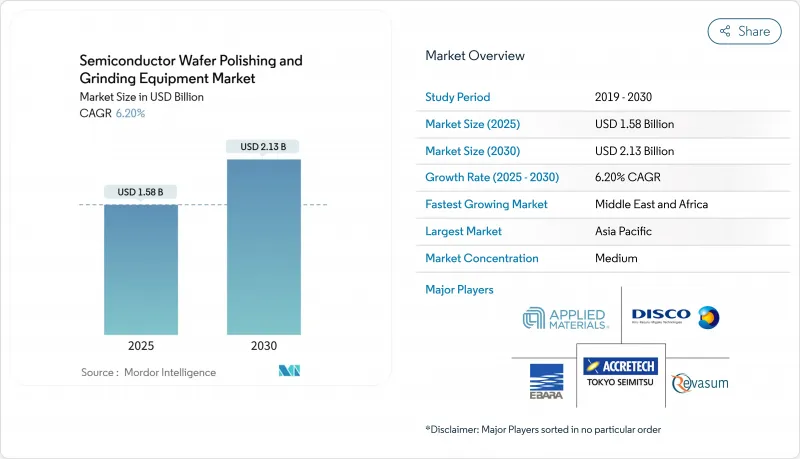
预计到 2025 年,半导体晶圆抛光和研磨设备市场规模将达到 15.8 亿美元,到 2030 年将达到 21.3 亿美元。
在此期间,对更大尺寸晶圆、宽能带隙材料和自动化工具的资本投资推动了精密材料移除系统订单量的持续成长。设备供应商扩展了即时製程控制能力,以实现原子级公差管理,而人工智慧诊断技术则弥补了工程师短缺并提高了产量比率。出口限制重塑了筹资策略,同时在北美和欧洲的同步投资降低了对亚洲的过度依赖,并增强了各地区的服务能力。永续性要求也影响了工具的选择,加速了向无浆料化学机械抛光 (CMP)垫片和消费量研磨技术的转变。
全球半导体晶圆抛光研磨设备市场趋势及洞察
亚洲地区搭载先进节点晶片的家用电器消耗量不断成长
在中国、印度和东南亚,旗舰智慧型手机和人工智慧穿戴装置的快速普及正在加速对3纳米以下装置的需求,这些装置需要原子级光滑的晶圆表面和十亿分之一等级的缺陷密度。儘管出口许可证存在不不确定性,但当地代工厂已扩大了其化学机械抛光(CMP)和精密研磨能力,工具製造商也推出了符合严格环保法规且不影响平整度的无氯垫片。多核心SoC的普及使得不同材料堆迭的製程一致性至关重要,从而推动了对可针对不同层进行调整的自适应控制CMP系统的投资。
小型化推动了对 300 毫米和 450 毫米 CMP 工具的需求。
为了追求成本效益高的晶粒密度,300mm 晶片尺寸成为主流,但随着更大尺寸的坯料使晶粒面积增加 2.25 倍,450mm 晶片的研发再次兴起。模具製造商透过加固压板、优化浆料分布以及引入原位计量技术来应对尺寸缩小带来的挑战,从而在大面积表面上保持奈米级的去除均匀性。台积电的 510mm x 515mm 矩形基板原型则提出了另一种无需彻底改造传统模具结构即可将可用面积扩大三倍的途径。
300毫米刀具的资本成本高,投资回报週期长。
到2024年,一台300毫米CMP平台的售价将达到300万至500万美元,设备升级还将额外花费100万至200万美元,这意味着对于产量较小的晶圆厂而言,投资回收期将超过四年。规模较小的晶圆厂推迟了扩张计划,转而选择维修或共享产能模式,儘管规模化生产具有明显的晶粒晶片成本优势,但整体设备普及速度仍然放缓。
细分市场分析
2024年,CMP设备占总收入的56.4%,并且仍然是实现先进节点平整度目标(需要0.1nm或更低的去除精度)的关键。随着晶圆厂采用无磨料浆料和人工智慧辅助的终点检测技术来提高3nm以下良率,半导体晶圆抛光和研磨设备市场也从中受益。整合式研磨机抛光平台减少了晶圆搬运次数,降低了颗粒风险,并缩短了等待产量比率。
到2030年,整合式研磨系统将以7.9%的复合年增长率超越独立式研磨机,因为客户会整合製程步骤以释放无尘室空间。供应商将闭合迴路温度控制、预测性维护和耗材寿命分析等功能捆绑在一起,以提高多品种生产的整体设备效率(OEE)。用于钻石和其他超硬基板的研磨和切割工具的出现,拓展了半导体晶圆抛光和研磨设备市场,使其延伸到光电和量子装置等细分领域。
300mm节点占了62.4%的市场收入,这得益于数十年的製程成熟度、优化的耗材以及折旧免税额的晶圆厂资产。 CMP垫片纹理和研磨几何形状的持续改进进一步提高了生产效率,巩固了该细分市场在半导体晶圆抛光和研磨设备市场中的经济主导地位。
相反,450mm及以上规格的晶圆尺寸实现了11.2%的最快复合年增长率,这主要得益于探索矩形晶圆规格的试点生产线,该规格有望使每片晶圆的晶粒增加3倍。设备製造商正在研发更大尺寸的压板以适应多种直径,并开发机器人搬运系统和大容量浆料输送系统,随着半导体晶圆抛光和研磨设备行业规模的扩大和投资回报率的评估,该行业预计将在2028年及以后实现大规模应用。
半导体晶圆抛光和研磨设备市场按设备类型(晶圆磨床、其他)、晶圆尺寸(小于 150 毫米、200 毫米、300 毫米、450 毫米及以上)、技术(研磨、其他)、半导体类型(记忆体、逻辑晶片、SoC、其他)、最终用户(集成设备製造商、其他细分市场)(记忆体、欧洲晶片、SoC、其他)、最终用户(整合装置製造商、其他细分市场)。
区域分析
到2024年,亚太地区将占全球收入的68.5%,其中台湾、韩国、日本和中国将引领市场。在台湾,集成设备蓝图和不断扩张的晶圆代工厂正在推动设备采购。台积电推出的无氯垫片以及日本的补贴支持型晶圆厂丛集,进一步强化了该地区对环保设备的偏好。出口限制的不确定性促使中国晶圆厂转向本地供应商,而高端CMP设备的进口则透过许可证豁免得以继续,从而维持了半导体晶圆抛光和研磨设备市场的基本需求。
自2022年《晶片与科学法案》颁布以来,北美经历了投资復兴。该法案注入了520亿美元的激励资金,并促使宣布到2025年将建造90多个晶圆厂,总价值约4,500亿美元。预计到2030年将出现6.7万名工程师的缺口,这使得自动化成为更高的优先事项,并推动了与学术联盟的合作,以加快人才培养。
欧洲颁布了一项价值 430 亿欧元(498.3 亿美元)的晶片法,目标是到 2030 年占据全球晶片产量的 20%。一家德国精密工程公司、一家法国先进封装中心和一家北欧材料科学研究所要求采购配备能源回收泵和水循环迴路的 CMP 系统,这使得采购符合欧盟绿色交易的目标,并促进了差异化的半导体晶圆抛光和研磨设备市场解决方案的发展。
其他福利:
- Excel格式的市场预测(ME)表
- 3个月的分析师支持
目录
第一章 引言
- 研究假设和市场定义
- 调查范围
第二章调查方法
第三章执行摘要
第四章 市场情势
- 市场概览
- 市场驱动因素
- 亚洲地区搭载尖端晶片的家用电器消耗量不断成长
- 受小型化趋势驱动,对 300 毫米和 450 毫米 CMP 工具的需求不断增长。
- 根据《晶片製造和升级法案》(CHIPS Act)对美国和欧洲晶圆代工产能的投资
- 向SiC/GaN功率元件的过渡需要超精密研磨。
- 3D-IC和异质整合中的产量比率提升需求
- 永续性要求推动无浆抛光技术进步
- 市场限制
- 300毫米刀具的资本成本高,投资回报週期长。
- 耗材成本上涨(垫片、浆料、钻石砂轮)
- 出口管制和智慧财产权壁垒限制了对中国的货物运输。
- 缺乏工艺设置和维护方面的熟练技术人员
- 价值链分析
- 监管或技术前景
- 波特五力模型
- 新进入者的威胁
- 买方的议价能力
- 供应商的议价能力
- 替代品的威胁
- 竞争对手之间的竞争
- 产业价值链分析
- 二手设备市场动态
- 投资分析
- 宏观经济影响评估
第五章 市场规模与成长预测
- 透过装置
- 晶圆研磨机
- 晶圆抛光(CMP)设备
- 多功能研磨机抛光工具
- 其他(包装,切薄)
- 按晶圆尺寸
- 150毫米或更小
- 200 mm
- 300 mm
- 450毫米或以上
- 透过技术
- 研磨
- 双面研磨
- 化学机械抛光(CMP)
- 边缘研磨和斜面抛光
- 依半导体类型
- 记忆体(DRAM、NAND)
- 逻辑电路和片上系统
- 功率和类比(Si、SiC、GaN)
- 微机电系统和感测器
- CMOS影像感测器
- LED和光电子学
- 最终用户
- 晶圆代工厂
- 整合装置製造商(IDM)
- OSAT/先进包装设施
- 研发机构及试验生产线
- 按地区
- 北美洲
- 美国
- 加拿大
- 南美洲
- 巴西
- 其他南美洲
- 欧洲
- 德国
- 英国
- 法国
- 义大利
- 其他欧洲地区
- 亚太地区
- 中国
- 台湾
- 日本
- 韩国
- 印度
- 亚太其他地区
- 中东和非洲
- 中东
- 沙乌地阿拉伯
- 阿拉伯聯合大公国
- 土耳其
- 其他中东地区
- 非洲
- 南非
- 奈及利亚
- 其他非洲地区
- 北美洲
第六章 竞争情势
- 市场集中度
- 策略趋势
- 市占率分析
- 公司简介
- Applied Materials Inc.
- Ebara Corporation
- DISCO Corporation
- Tokyo Seimitsu Co. Ltd(ACCRETECH)
- Revasum Inc.
- Komatsu NTC Ltd.
- Okamoto Machine Tool Works Co. Ltd.
- Lapmaster Wolters GmbH(Precision Surfacing Solutions)
- Logitech Ltd.
- Entrepix Inc.(Amtech Systems)
- G&N Genauigkeits Maschinenbau Nurnberg GmbH
- Hantop Intelligence Tech Co. Ltd.
- CMP-Tec Inc.
- Koyo Machinery Co. Ltd.
- Shanghai ShinEne Technology Co. Ltd.
- Qingdao Lapping & Polishing Equipment Co. Ltd.
- Nagase Integrex Co. Ltd.
- Strausbaugh Inc.(S-Cubed)
- Pureon AG
- Vibrantz Technologies Inc.
- Axus Technology
- SHANGHAI FAMOUS TRADE CO.,LTD(ZMSH)
- Huahai Machinery Group
- Hansung Engineering Co. Ltd.
- GPMT Co. Ltd.
第七章 市场机会与未来展望
The semiconductor wafer polishing and grinding equipment market size stood at USD 1.58 billion in 2025 and is forecast to reach USD 2.13 billion by 2030, reflecting a 6.2% CAGR as device makers pursue smaller geometries and higher performance.
During the period, capital spending on larger wafers, wide-bandgap materials, and automation tools has driven sustained order volumes for precision material-removal systems. Equipment suppliers scaled real-time process-control features to manage atomic-level tolerances, while AI-enabled diagnostics offset technician shortages and improved yield. Export-control rules reshaped sourcing strategies, prompting parallel investments in North America and Europe that reduced over-reliance on Asia and strengthened regional service footprints. Sustainability mandates also influenced tool selection, accelerating the shift toward slurry-free CMP pads and low-consumable grinding technologies.
Global Semiconductor Wafer Polishing And Grinding Equipment Market Trends and Insights
Growing consumption of consumer electronics with advanced-node chips in Asia
Rapid uptake of flagship smartphones and AI-enabled wearables across China, India, and Southeast Asia accelerated demand for sub-3 nm devices that require atomically smooth wafer surfaces and defect densities measured in parts per billion. Local foundries expanded CMP and fine-grinding capacity despite export-license uncertainty, while tool makers introduced chlorine-free pads that met strict environmental codes without compromising planarity. As multi-core SoCs proliferated, process uniformity across diverse material stacks became critical, spurring investment in adaptive-control CMP systems tailored for heterogeneous layers.
Miniaturization push driving demand for 300 mm and 450 mm CMP tools
The search for cost-effective die density sustained 300 mm as the mainstream format, yet exploratory 450 mm development resurfaced because a larger blank yields 2.25 times more die area. Tool makers tackled the scale-up challenge by reinforcing platens, optimizing slurry distribution, and embedding in-situ metrology to maintain nanometer-level removal uniformity across wider surfaces. TSMC's prototype 510 mm X 515 mm rectangular substrate hinted at an alternate path that could triple usable area without fully overhauling legacy tool architectures.
High capital cost and long ROI cycle for 300 mm tools
A single 300 mm CMP platform carried a USD 3-5 million price tag in 2024, with facility upgrades adding USD 1-2 million, stretching payback beyond 4 years in lower-volume fabs. Smaller players delayed expansion and opted for refurbished or shared-capacity models, slowing overall tool uptake despite clear cost-per-die advantages at scale.
Other drivers and restraints analyzed in the detailed report include:
- Foundry capacity investments in the U.S. and Europe under the CHIPS Act
- Transition to SiC/GaN power devices requires ultra-precision grinding
- Export controls and IP barriers limiting shipments to China
For complete list of drivers and restraints, kindly check the Table Of Contents.
Segment Analysis
CMP tools generated 56.4% of 2024 revenue and remained central to advanced-node planarity targets that mandate removal accuracy below 0.1 nm. The semiconductor wafer polishing and grinding equipment market benefited as fabs adopted abrasive-free slurries and AI-assisted endpoint detection to push sub-3 nm yields upward. Integrated grinder-polisher platforms reduced wafer transfers, trimming particle risks, and cutting queue time.
Integrated systems' 7.9% CAGR through 2030 outpaced standalone grinders as customers consolidated process steps to free cleanroom space. Vendors bundled closed-loop temperature control, predictive maintenance, and consumable-life analytics, enhancing OEE for high-mix production. Emerging lapping and slicing tools addressed diamond and other ultra-hard substrates, extending the semiconductor wafer polishing and grinding equipment market reach into niche photonics and quantum-device lines.
The 300 mm node held 62.4% of market revenue, underlining decades of process maturity, optimized consumables, and well-depreciated fab assets. Continuous enhancements in CMP pad texture and back-grinding wheel geometry further raised throughput, reinforcing the segment's economic moat within the semiconductor wafer polishing and grinding equipment market.
Conversely, the 450 mm and above category registered the fastest 11.2% CAGR, driven by pilot lines exploring rectangular formats that promise 3X more die per wafer. Equipment makers prototyped enlarged platens, robotic handlers, and high-capacity slurry-delivery systems adaptable to multiple diameters, positioning themselves for potential mass adoption beyond 2028 as the semiconductor wafer polishing and grinding equipment industry evaluates ROI at scale.
Semiconductor Wafer Polishing and Grinding Equipment Market is Segmented by Equipment Type (Wafer Grinding Machines, and More), Wafer Size (<=150 Mm, 200 Mm, 300 Mm, and 450 Mm and Above), Technology (Back-Grinding, and More), Semiconductor Type (Memory, Logic and SoC, and More), End-User (Integrated Device Manufacturers, and More), and Geography (North America, South America, Europe, Asia-Pacific, and Middle East and Africa).
Geography Analysis
Asia-Pacific retained 68.5% of global revenue in 2024, anchored by Taiwan, South Korea, Japan, and China, where integrated device roadmaps and foundry expansions sustained tool procurements. TSMC's chlorine-free pad rollout and Japan's subsidy-backed fab clusters reinforced a regional preference for environmentally optimized equipment. Export-control uncertainties nudged Chinese fabs to local suppliers, yet high-end CMP imports persisted via license exceptions, preserving baseline semiconductor wafer polishing and grinding equipment market demand.
North America experienced an investment renaissance following the 2022 CHIPS and Science Act, which mobilized USD 52 billion in incentives and prompted over 90 fab announcements worth nearly USD 450 billion through 2025. Capacity additions raised tool orders, although technician gaps of 67,000 positions by 2030 drove automation priorities and partnerships with academic consortia to accelerate workforce pipelines.
Europe followed with the EUR 43 billion (USD 49.83 billion) Chips Act that targeted a 20% global output share by 2030. Germany's precision-engineering firms, France's advanced-packaging hubs, and Nordic material-science institutes demanded CMP systems featuring energy-recovery pumps and water-recycling loops, aligning procurement with EU Green Deal objectives and fostering differentiated semiconductor wafer polishing and grinding equipment market solutions.
- Applied Materials Inc.
- Ebara Corporation
- DISCO Corporation
- Tokyo Seimitsu Co. Ltd (ACCRETECH)
- Revasum Inc.
- Komatsu NTC Ltd.
- Okamoto Machine Tool Works Co. Ltd.
- Lapmaster Wolters GmbH (Precision Surfacing Solutions)
- Logitech Ltd.
- Entrepix Inc. (Amtech Systems)
- G&N Genauigkeits Maschinenbau Nurnberg GmbH
- Hantop Intelligence Tech Co. Ltd.
- CMP-Tec Inc.
- Koyo Machinery Co. Ltd.
- Shanghai ShinEne Technology Co. Ltd.
- Qingdao Lapping & Polishing Equipment Co. Ltd.
- Nagase Integrex Co. Ltd.
- Strausbaugh Inc. (S-Cubed)
- Pureon AG
- Vibrantz Technologies Inc.
- Axus Technology
- SHANGHAI FAMOUS TRADE CO.,LTD (ZMSH)
- Huahai Machinery Group
- Hansung Engineering Co. Ltd.
- GPMT Co. Ltd.
Additional Benefits:
- The market estimate (ME) sheet in Excel format
- 3 months of analyst support
TABLE OF CONTENTS
1 INTRODUCTION
- 1.1 Study Assumptions and Market Definition
- 1.2 Scope of the Study
2 RESEARCH METHODOLOGY
3 EXECUTIVE SUMMARY
4 MARKET LANDSCAPE
- 4.1 Market Overview
- 4.2 Market Drivers
- 4.2.1 Growing Consumption of Consumer Electronics with Advanced-Node Chips in Asia
- 4.2.2 Miniaturization Push Driving Demand for 300 mm and 450 mm CMP Tools
- 4.2.3 Foundry Capacity Investments in U.S. and Europe under CHIPS Acts
- 4.2.4 Transition to SiC/GaN Power Devices Requiring Ultra-Precision Grinding
- 4.2.5 Yield-Enhancement Needs for 3D-IC and Heterogeneous Integration
- 4.2.6 Sustainability Mandates Advancing Slurry-Free Polishing Technologies
- 4.3 Market Restraints
- 4.3.1 High Capital Cost and Long ROI Cycle for 300 mm Tools
- 4.3.2 Consumables Cost Inflation (Pads, Slurries, Diamond Wheels)
- 4.3.3 Export-Control and IP Barriers Limiting Shipments to China
- 4.3.4 Skilled-Technician Shortage for Process Set-up and Maintenance
- 4.4 Value Chain Analysis
- 4.5 Regulatory or Technological Outlook
- 4.6 Porter's Five Forces
- 4.6.1 Threat of New Entrants
- 4.6.2 Bargaining Power of Buyers
- 4.6.3 Bargaining Power of Suppliers
- 4.6.4 Threat of Substitute Products
- 4.6.5 Intensity of Competitive Rivalry
- 4.7 Industry Value Chain Analysis
- 4.8 Secondary Equipment Market Dynamics
- 4.9 Investment Analysis
- 4.10 Macroeconomic Impact Assessment
5 MARKET SIZE AND GROWTH FORECASTS (VALUE)
- 5.1 By Equipment Type
- 5.1.1 Wafer Grinding Machines
- 5.1.2 Wafer Polishing (CMP) Equipment
- 5.1.3 Integrated Grinder-Polisher Tools
- 5.1.4 Others (Lapping, Slicing Thinners)
- 5.2 By Wafer Size
- 5.2.1 <=150 mm
- 5.2.2 200 mm
- 5.2.3 300 mm
- 5.2.4 450 mm and Above
- 5.3 By Technology
- 5.3.1 Back-Grinding
- 5.3.2 Double-Side Grinding
- 5.3.3 Chemical Mechanical Polishing (CMP)
- 5.3.4 Edge-Grinding / Bevel Polishing
- 5.4 By Semiconductor Type
- 5.4.1 Memory (DRAM, NAND)
- 5.4.2 Logic and SoC
- 5.4.3 Power and Analog (Si, SiC, GaN)
- 5.4.4 MEMS and Sensors
- 5.4.5 CMOS Image Sensors
- 5.4.6 LED and Optoelectronics
- 5.5 By End-User
- 5.5.1 Foundries
- 5.5.2 Integrated Device Manufacturers (IDMs)
- 5.5.3 OSAT / Advanced Packaging Facilities
- 5.5.4 Research and Development Institutes and Pilot Lines
- 5.6 By Geography
- 5.6.1 North America
- 5.6.1.1 United States
- 5.6.1.2 Canada
- 5.6.2 South America
- 5.6.2.1 Brazil
- 5.6.2.2 Rest of South America
- 5.6.3 Europe
- 5.6.3.1 Germany
- 5.6.3.2 United Kingdom
- 5.6.3.3 France
- 5.6.3.4 Italy
- 5.6.3.5 Rest of Europe
- 5.6.4 Asia-Pacific
- 5.6.4.1 China
- 5.6.4.2 Taiwan
- 5.6.4.3 Japan
- 5.6.4.4 South Korea
- 5.6.4.5 India
- 5.6.4.6 Rest of Asia-Pacific
- 5.6.5 Middle East and Africa
- 5.6.5.1 Middle East
- 5.6.5.1.1 Saudi Arabia
- 5.6.5.1.2 United Arab Emirates
- 5.6.5.1.3 Turkey
- 5.6.5.1.4 Rest of Middle East
- 5.6.5.2 Africa
- 5.6.5.2.1 South Africa
- 5.6.5.2.2 Nigeria
- 5.6.5.2.3 Rest of Africa
- 5.6.1 North America
6 COMPETITIVE LANDSCAPE
- 6.1 Market Concentration
- 6.2 Strategic Moves
- 6.3 Market Share Analysis
- 6.4 Company Profiles (includes Global-level Overview, Market-level Overview, Core Segments, Financials, Strategic Information, Market Rank/Share, Products and Services, Recent Developments)
- 6.4.1 Applied Materials Inc.
- 6.4.2 Ebara Corporation
- 6.4.3 DISCO Corporation
- 6.4.4 Tokyo Seimitsu Co. Ltd (ACCRETECH)
- 6.4.5 Revasum Inc.
- 6.4.6 Komatsu NTC Ltd.
- 6.4.7 Okamoto Machine Tool Works Co. Ltd.
- 6.4.8 Lapmaster Wolters GmbH (Precision Surfacing Solutions)
- 6.4.9 Logitech Ltd.
- 6.4.10 Entrepix Inc. (Amtech Systems)
- 6.4.11 G&N Genauigkeits Maschinenbau Nurnberg GmbH
- 6.4.12 Hantop Intelligence Tech Co. Ltd.
- 6.4.13 CMP-Tec Inc.
- 6.4.14 Koyo Machinery Co. Ltd.
- 6.4.15 Shanghai ShinEne Technology Co. Ltd.
- 6.4.16 Qingdao Lapping & Polishing Equipment Co. Ltd.
- 6.4.17 Nagase Integrex Co. Ltd.
- 6.4.18 Strausbaugh Inc. (S-Cubed)
- 6.4.19 Pureon AG
- 6.4.20 Vibrantz Technologies Inc.
- 6.4.21 Axus Technology
- 6.4.22 SHANGHAI FAMOUS TRADE CO.,LTD (ZMSH)
- 6.4.23 Huahai Machinery Group
- 6.4.24 Hansung Engineering Co. Ltd.
- 6.4.25 GPMT Co. Ltd.
7 MARKET OPPORTUNITIES AND FUTURE OUTLOOK
- 7.1 White-space and Unmet-Need Assessment
 2032年半导体晶圆抛光和研磨设备市场预测:按设备类型、晶圆尺寸、技术节点、半导体类型、应用和地区的全球分析
 全球半导体抛光垫片市场全球半导体晶圆抛光研磨设备市场
 2025 年至 2033 年半导体晶圆抛光和研磨设备市场报告(按类型(半导体晶圆抛光设备、半导体晶圆研磨设备)、最终用户(代工厂、内存製造商、IDM 等)和地区)
 半导体晶圆抛光和研磨设备市场按设备类型、晶圆尺寸、应用和最终用户划分 - 2025 年至 2030 年全球预测
 2025 年至 2035 年全球半导体晶圆抛光研磨设备市场半导体晶圆抛光和研磨设备市场规模、份额、趋势分析报告:按产品、晶圆尺寸、最终用途、地区和细分市场进行预测,2025 年至 2030 年
 半导体抛光垫市场,按类型、按应用、按材料、按国家和地区 - 2025 年至 2032 年全球行业分析、市场规模、市场份额和预测半导体晶圆抛光和研磨设备市场,按应用、最终用户、国家和地区划分 - 2024-2032 年行业分析、市场规模、市场份额和预测
 2024-2028年全球半导体晶圆抛光研磨设备市场