


 |
市场调查报告书
商品编码
1549780
高端半导体封装:市场占有率分析、产业趋势与统计、成长预测(2024-2029)High-end Semiconductor Packaging - Market Share Analysis, Industry Trends & Statistics, Growth Forecasts (2024 - 2029) |
||||||
※ 本网页内容可能与最新版本有所差异。详细情况请与我们联繫。
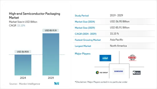
高端半导体封装市场规模预计2024年为369.5亿美元,预计2029年将达到859.1亿美元,在预测期内(2024-2029年)复合年增长率预计为15.10%。
随着封装越来越多地用于提高电子系统的性能、可靠性和成本效益,行业中各个最终用户垂直领域的需求不断增加,整合、能源效率和产品性能的不断发展正在加速市场成长。
主要亮点
- 包装可保护电子系统免受高频噪音辐射、静电放电、机械损坏和冷却的影响。全球半导体产业的成长是推动半导体封装市场成长的主要因素之一。此外,2023年2月,半导体产业协会(SIA)宣布,2022年全球半导体产业销售额将达到5,741亿美元,创历史最高年度总合,比前一年公布的5,559亿美元成长3.3%。
- 此外,物联网和人工智慧的兴起以及复杂电子设备的激增正在推动消费性电子和汽车行业的高端应用。这些因素正在推动更先进的半导体封装技术来维持需求。该领域研究活动的活性化进一步刺激了市场需求。
- 此外,由于 5G、物联网、汽车和 HPC 等多个长期成长驱动因素,半导体封装市场预计将扩大。例如,印度政府已核准一项100亿美元的奖励计划,以建立包括晶圆厂、本土晶片设计和化合物半导体晶圆厂在内的完整半导体生态系统。
- 此外,COVID-19大流行对电子产业产生了重大影响,半导体供应链问题和晶片短缺已经影响该产业一段时间。然而,全球半导体产业投资的增加和半导体製造设施的增加预计将推动后疫情时代的市场成长。
高端半导体封装市场趋势
消费性电子产业可望提振市场
- 消费性电子领域正大力投资半导体封装市场。智慧型手机的成长、穿戴式装置和智慧型装置的渗透率不断提高,以及消费者物联网装置在智慧家庭等应用中的渗透率不断提高,是影响该细分市场成长的一些因素。爱立信预计,2022年全球智慧型手机行动网路用户数量预计将达到约66亿,2028年将超过78亿人。
- 此外,由于复杂的半导体元件可以提供越来越多的功能和特性,智慧型手錶和智慧扬声器市场近年来变得非常受欢迎。因此,对Wi-Fi和蓝牙晶片的需求急剧增加。消费性电子製造商也利用半导体元件为其产品配备物联网和人工智慧模型,以改善用户体验并为产品增添光彩。
- 例如,2023年3月,华为计画在未来几年推出一款电池大幅升级的折迭式智慧型手机。该设备具有电池升级功能。此外,华为预计将采用高硅负极材料来增强智慧型手机的电池容量,预计电池容量将达到5,060mAh。
- 电脑和笔记型电脑现已成为大力投资科技的年轻消费者的必需品。此外,电子领域的技术创新和进步预计将在未来 10 年推动半导体封装销售。物联网和人工智慧的引入预计将增加全球新兴市场和已开发市场的半导体封装销售。
- 英特尔公司和伦敦大学学院 (UCL) 联合推出了一款新型非接触式计算机,可以使用手部和脸部手势进行操作和控制。电子市场不断要求更高的功耗、更高的速度、更多的引脚数、更小的占地面积和更薄的设计。半导体的小型化和整合化正在创造更轻、更小、更便携的家用电器,例如智慧型手机、平板电脑和新兴的物联网设备。
北美市场正在经历显着成长
- 美国和加拿大的半导体产业在人工智慧、量子运算和 5G 等先进无线网路等未来关键技术中保持着重要地位。
- 例如,根据GSMA的预测,2025年5G将成为美国领先的网路技术。 5G 网路部署的不断增加,恰逢对更即时、高效能运算设备的需求不断增长,其中半导体是关键要素。
- 美国政府正在大力投资以促进先进技术的采用,从而增强对先进半导体封装的需求。美国参议院宣布了促进美国製造半导体(FABS)法案。该法案可为半导体製造设备和工厂的投资提供 25% 的投资税额扣抵。
- 此外,美国是最大的电动车市场之一,近年来电动车销量快速成长。汽车创新联盟的数据显示,2023年第四季国内电动车销量超过37.7万辆,较2022年第四季成长34%。
- 近年来,日本实施了多项法规来推广电动车的使用。例如,纽约州立法机关通过了一项法案,实际上要求到 2035 年该州销售的所有新乘用车都必须采用电力驱动。此外,美国也制定了2030年该国销售的汽车一半为电动车的目标。
高端半导体封装产业概况
高端半导体封装市场正在整合。公司正在利用产品创新、扩张和合作伙伴关係来在竞争中生存并扩大市场范围。
- 2024 年 5 月 着名的半导体封装测试公司 Siliconware Precision Industries (SPIL) 最近在槟城决明城科技园区开设了马来西亚 P1 工厂。未来15年,SPIL计划部署包括晶圆凸点在内的新技术,并提供全面的承包解决方案,包括晶圆凸点、晶圆级晶片封装、覆晶构装和测试。
- 2024 年 3 月,韩国 Nepes Corporation 将与西门子 EDA 合作,解决先进 3D-IC 封装中复杂的热学、机械和IC封装设计挑战。 Nepes 专注于晶圆级、扇出晶圆级和麵板级封装设计。 Nepes 利用其专业知识,利用西门子 EDA 技术(包括 Calibre nmPlatform、HyperLynx 和 Xpedition 软体)来推动包装创新。透过整合这些西门子解决方案,Nepes将能够增强其设计能力,并为全球IC客户提供快速可靠的2.5D/3D小晶片设计服务。
其他好处
- Excel 格式的市场预测 (ME) 表
- 3 个月分析师支持
目录
第一章简介
- 研究假设和市场定义
- 调查范围
第二章调查方法
第三章执行摘要
第四章市场洞察
- 市场概况
- 产业吸引力-波特五力分析
- 供应商的议价能力
- 买方议价能力
- 新进入者的威胁
- 替代品的威胁
- 竞争公司之间敌对关係的强度
- 产业价值链分析
- 评估宏观经济趋势对市场的影响
第五章市场动态
- 市场驱动因素
- 各行业半导体元件消费扩大
- 扩大 3D 列印在半导体封装的应用
- 市场限制因素
- 半导体IC设计初始投资高且复杂
第六章 市场细分
- 依技术
- 3D SoC
- 3D堆迭内存
- 2.5D中介层
- UHD FO(超高密度扇出)
- 内置硅桥
- 按最终用户
- 家用电子产品
- 航太/国防
- 医疗设备
- 电讯
- 车
- 其他最终用户
- 按地区
- 北美洲
- 美国
- 加拿大
- 欧洲
- 英国
- 德国
- 法国
- 义大利
- 亚洲
- 中国
- 印度
- 日本
- 澳洲/纽西兰
- 东南亚
- 拉丁美洲
- 中东/非洲
- 北美洲
第七章 竞争格局
- 公司简介
- Intel Corporation
- Taiwan Semiconductor Manufacturing Company
- Advanced Semiconductor Engineering Inc.
- Samsung Electronics Co. Ltd
- Amkor Technology Inc.
- JCET Group Co. Ltd
- TongFu Microelectronics Co. Ltd
- Fujitsu Limited
- Siliconware Precision Industries Co. Ltd
- Powertech Technology Inc.
第八章投资分析
第9章市场的未来
The High-end Semiconductor Packaging Market size is estimated at USD 36.95 billion in 2024, and is expected to reach USD 85.91 billion by 2029, growing at a CAGR of 15.10% during the forecast period (2024-2029).
The continuous advancements in integration, energy efficiency, and product characteristics because of the growing demand across various end-user verticals of the industry and the use of packaging for improving the performance, reliability, and cost-effectiveness of electronic systems accelerate the market's growth.
Key Highlights
- Packaging protects an electronic system from radio frequency noise emission, electrostatic discharge, mechanical damage, and cooling. The rise in the semiconductor industry worldwide is one of the major factors driving the growth of the semiconductor packaging market. In addition, in February 2023, the Semiconductor Industry Association (SIA) announced global semiconductor industry sales totaled USD 574.1 billion in 2022, the highest-ever annual total and an increase of 3.3% compared to the previous year's total of USD 555.9 billion.
- Furthermore, the rise of IoT and AI and the proliferation of complex electronics drive the high-end application segment in the consumer electronics and automotive industries. Due to these factors, more advanced semiconductor packaging technologies are being adopted to sustain demand. The growing research activities in the sector further bolstered the market's demand.
- Furthermore, the semiconductor packaging market is expected to expand due to multiple long-term growth drivers, like 5G, IoT, automotive, and HPC. For instance, the Government of India approved a USD 10 billion incentive package to build a complete semiconductor ecosystem, including fabs, home-grown chip design, and compound semiconductor plants.
- Moreover, the COVID-19 pandemic significantly impacted the electronics industry, with semiconductor supply chain issues and the chip shortage affecting the industry for some time. However, the growing investments in the semiconductor industry and increased establishments of semiconductor manufacturing facilities worldwide are anticipated to propel the market's growth in the post-pandemic era.
High-end Semiconductor Packaging Market Trends
Consumer Electronics Sector is Expected to Boost the Market
- The consumer electronics sector is significantly investing in the semiconductor packaging market. Growth of the smartphone, rising wearable and smart device adoption, and increasing consumer IoT device penetration in applications like smart homes are a few of the influential factors influencing the segment's growth. According to Ericsson, smartphone mobile network subscriptions worldwide reached nearly 6.6 billion in 2022, and they are predicted to exceed 7.8 billion by 2028.
- Additionally, markets for smartwatches and smart speakers have become extremely popular in recent years due to the growing number of features and functionalities they can offer due to sophisticated semiconductor components. As a result, the demand for Wi-Fi and Bluetooth chips increased dramatically. Consumer electronics manufacturers also use semiconductor components to equip their products with IoT and AI models, enhancing user experience and making products brighter.
- For instance, in March 2023, Huawei planned to launch its foldable smartphone with a significant battery upgrade in the coming years. The device will feature an upgrade to its battery. Further, Huawei is expected to use a high-silicon anode material to enhance the smartphone's battery capacity, which is expected to be 5,060 mAh.
- Personal computers and laptops are now essential for young consumers who are heavily invested in technology. In addition, over the next ten years, innovation and advancement in the electronics sector are anticipated to drive semiconductor packaging sales. Sales of semiconductor packaging are expected to increase globally in both developing and developed markets due to the introduction of IoT and AI.
- Intel Corporation and the University College London (UCL) have collaborated to introduce a new touchless computer that can be operated and controlled by gesturing the hands and face. Higher power dissipation, faster speeds, higher pin counts, smaller footprints, and lower profiles are all constant demands in the electronics market. Semiconductor miniaturization and integration have resulted in lighter, smaller, and more portable appliances such as smartphones, tablets, and emerging IoT devices.
North America to Experience Significant Market Growth
- The semiconductor sector in the United States and Canada has maintained a significant position in key future technologies, such as AI, quantum computing, and sophisticated wireless networks like 5G.
- For instance, as per GSMA, 5G will become the lead network technology in the United States by 2025. The increasing implementation of 5G networks coincides with the growing demand for more immediate high-performance computing appliances, for which semiconductors form a critical element.
- The US government has significantly invested in boosting the penetration of advanced technologies, bolstering the demand for high-end semiconductor packaging. The US Senate announced the Facilitating American-Built Semiconductors (FABS) Act, which may provide tax incentives to semiconductor manufacturers. The bill may establish a 25% investment tax credit for semiconductor manufacturing investments in equipment or fabs.
- Furthermore, the United States is one of the largest markets for electric vehicles, and the country has also recorded rapid growth in EV sales in recent years. More than 377,000 EVs were sold in the country in Q4 2023, registering a 34% increase from Q4 2022, according to Alliance for Automotive Innovation.
- Many regulations have been implemented in recent years to promote the use of electric vehicles in the country. For instance, New York state lawmakers passed a bill that essentially mandates that all new passenger cars sold in the state run on electric power by 2035. Moreover, the United States has set a target to ensure half of the vehicles sold in the country are electric by 2030.
High-end Semiconductor Packaging Industry Overview
The high-end semiconductor packaging market is consolidated. Companies employ product innovation, expansions, and partnerships to stay ahead of the competition and widen their market reach.
- May 2024: Siliconware Precision Industries Co. Ltd (SPIL), a prominent player in semiconductor packaging and testing, recently marked the commencement of its Malaysia P1 plant at Bandar Cassia Technology Park, Pulau Pinang. Over the next 15 years, SPIL plans to roll out new technologies, including wafer bumping, and provide a holistic turnkey solution encompassing wafer bumping, wafer-level chip packaging, flip chip packaging, and testing.
- March 2024: Nepes Corporation in South Korea partnered with Siemens EDA to address complex thermal, mechanical, and IC packaging design challenges in advanced 3D-IC packages. Nepes specializes in wafer-level, fan-out wafer-level, and panel-level packaging designs. Expanding on its expertise, Nepes is driving packaging innovations using Siemens EDA's technologies, including the Calibre nmPlatform, HyperLynx, and Xpedition software. By integrating these Siemens solutions, Nepes has enhanced its design capabilities, enabling swift and dependable services in 2.5D/3D chiplet designs for its global IC clientele.
Additional Benefits:
- The market estimate (ME) sheet in Excel format
- 3 months of analyst support
TABLE OF CONTENTS
1 INTRODUCTION
- 1.1 Study Assumptions and Market Definitions
- 1.2 Scope of the Study
2 RESEARCH METHODOLOGY
3 EXECUTIVE SUMMARY
4 MARKET INSIGHTS
- 4.1 Market Overview
- 4.2 Industry Attractiveness - Porter's Five Forces Analysis
- 4.2.1 Bargaining Power of Suppliers
- 4.2.2 Bargaining Power of Buyers
- 4.2.3 Threat of New Entrants
- 4.2.4 Threat of Substitute Products
- 4.2.5 Intensity of Competitive Rivalry
- 4.3 Industry Value Chain Analysis
- 4.4 Assessment of the Impact of Macroeconomic Trends on the Market
5 MARKET DYNAMICS
- 5.1 Market Drivers
- 5.1.1 Growing Consumption of Semiconductor Devices Across Industries
- 5.1.2 Growing Adoption of 3D Printing in Semiconductor Packaging
- 5.2 Market Restraints
- 5.2.1 High Initial Investment and Increasing Complexity of Semiconductor IC Designs
6 MARKET SEGMENTATION
- 6.1 By Technology
- 6.1.1 3D SoC
- 6.1.2 3D Stacked Memory
- 6.1.3 2.5D interposers
- 6.1.4 UHD FO
- 6.1.5 Embedded Si Bridge
- 6.2 By End User
- 6.2.1 Consumer Electronics
- 6.2.2 Aerospace and Defense
- 6.2.3 Medical Devices
- 6.2.4 Telecom and Communication
- 6.2.5 Automotive
- 6.2.6 Other End Users
- 6.3 By Geography
- 6.3.1 North America
- 6.3.1.1 United States
- 6.3.1.2 Canada
- 6.3.2 Europe
- 6.3.2.1 United Kingdom
- 6.3.2.2 Germany
- 6.3.2.3 France
- 6.3.2.4 Italy
- 6.3.3 Asia
- 6.3.3.1 China
- 6.3.3.2 India
- 6.3.3.3 Japan
- 6.3.3.4 Australia and New Zealand
- 6.3.3.5 South East Asia
- 6.3.4 Latin America
- 6.3.5 Middle East and Africa
- 6.3.1 North America
7 COMPETITIVE LANDSCAPE
- 7.1 Company Profiles
- 7.1.1 Intel Corporation
- 7.1.2 Taiwan Semiconductor Manufacturing Company
- 7.1.3 Advanced Semiconductor Engineering Inc.
- 7.1.4 Samsung Electronics Co. Ltd
- 7.1.5 Amkor Technology Inc.
- 7.1.6 JCET Group Co. Ltd
- 7.1.7 TongFu Microelectronics Co. Ltd
- 7.1.8 Fujitsu Limited
- 7.1.9 Siliconware Precision Industries Co. Ltd
- 7.1.10 Powertech Technology Inc.
8 INVESTMENTS ANALYSIS
9 FUTURE OF THE MARKET
 全球半导体塑胶载带市场:实际结果与预测(2019-2030)
 先进半导体封装市场预测至 2030 年:按封装类型、装置类型、材料类型、技术、应用、最终用户和地区进行的全球分析
 3-D TSV:关键问题洞察与市场分析
 高密度封装(MCM、MCP、SIP、3D-TSV):市场分析与技术趋势
 2024 年先进晶片封装全球市场报告
 2030 年 3D TSV 封装市场预测:按产品类型、製程实现、技术、应用、最终用户和地区进行的全球分析
 2.5D/3D半导体封装的全球市场:市场占有率分析、产业趋势/统计、成长预测(2024-2029)
 半导体封装:市场占有率分析、产业趋势与统计、成长预测(2024-2029)
 3D TSV 封装市场报告:2030 年趋势、预测与竞争分析
 载带市场报告:2030 年趋势、预测与竞争分析