


 |
市场调查报告书
商品编码
1940553
先进积体电路基板:市场占有率分析、产业趋势与统计、成长预测(2026-2031)Advanced IC Substrates - Market Share Analysis, Industry Trends & Statistics, Growth Forecasts (2026 - 2031) |
||||||
※ 本网页内容可能与最新版本有所差异。详细情况请与我们联繫。
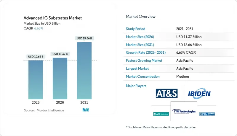
预计先进积体电路基板市场将从 2025 年的 106.6 亿美元成长到 2026 年的 113.7 亿美元,到 2031 年将达到 156.6 亿美元,2026 年至 2031 年的复合年增长率为 6.63%。
市场需求已从传统运算转向以人工智慧为中心的工作负载,这需要更高的层数、更细的线宽和更严格的翘曲控制。亚太地区的基板供应商受益于此转变,因为他们已经拥有强大的ABF产能,并与代工厂的封装生产线建立了紧密的合作关係。主要云端服务供应商将长期采购协议的期限提前至2025年,以确保CoWoS和FC-BGA的稳定供应,这进一步增强了基板製造商的定价权。同时,玻璃芯技术的发展日益成熟,为超高密度封装提供了一种替代ABF的策略选择,预计将在2020年代末期实现商业化。
全球先进积体电路基板市场趋势与洞察
AI/HPC加速器对ABF基板的需求快速成长
2025 代 AI 伺服器的大规模部署导致味之素增材製造膜 (ABF) 供应紧张。 ABF 面板的前置作业时间已超过 35 週,现货价格较 2024 年合约价格溢价高达 25%。台湾供应商 Unimicron、Kinsus 和南亚 PCB 在经历了长期的库存调整后,营收已恢復两位数成长,但为满足需求,其运转率仍维持在 90%。三星马达在 2025 年第二季提高了其 AI 伺服器的 ABF 产能,并开始试生产玻璃芯。这体现了其为降低单一材料风险而采取的双源策略。台积电已宣布计划将 CoWoS 的年产量翻一番,这意味着基板需求将显着超过现有产能。这些发展已使供不应求扩大至 20%,基板製造商预计这种短缺状况将持续到 2026 年新生产线运作为止。
几何缩放和异质整合的趋势
晶片组架构、无芯中介层和穿透硅通孔(TSV) 技术重新定义了封装设计规则,使生产环境中的基板线宽低于 10µm。应用材料公司强调,与单晶粒方案相比,封装内整合离散晶片组可实现更高的每瓦性能。凸版印刷推出了一种无芯有机中介层,其热膨胀係数比传统的 ABF 解决方案低 45%,从而降低了多晶片堆迭中的机械应力。博通公司的 3.5D XDSiP 技术将超过 6000mm² 的硅片整合到 12 层 HBM 堆迭中,凸显了对能够在有限面积内布线数千个高速讯号的基板的需求。台积电和日月光投资建造了尺寸高达 310x310mm 的面板级封装生产线,以提高步进马达效率并降低每平方英吋成本。这些变化正将先进 IC基板市场定位为实现下一代运算密度的关键基础技术。
ABF基板供不应求和前置作业时间突然延长
从2024年到2025年,ABF面板持续的供不应求阻碍了先进IC基板市场的发展。 ABF树脂的近乎垄断供应商味之素株式会社承认,在新的树脂反应器于2026年运作之前,供需缺口将达到20%。台积电表示其只能满足CoWoS需求的80%,证实了代工厂面临的限制。积水化学等竞争对手试图摆脱对积层製造的依赖,但高端AI封装的认证週期延缓了他们的实施。同时,因其低膨胀係数而备受青睐的T-Glass芯材的短缺,延缓了日东纺的产能扩张,并加剧了前置作业时间的延长。儘管基板製造商实施了在线连续计量以提高一次产量比率并优化现有产能,但大多数客户在2025年之前仍需遵守配额计画。
细分市场分析
到2025年,FC-BGA基板占据了先进IC基板市场44.32%的份额。其主导地位源自于其久经考验的电气性能,而这正是AI加速器和伺服器CPU所必需的。由于GPU製造商竞相确保产能,FC - BGA基板的运转率在2025年全年保持高位。然而,成长重心转向了用于汽车网域控制器和折迭式行动装置的刚挠性CSP生产线。软硬复合CSP的出货量以7.94%的复合年增长率成长,吸引了能够平衡弯曲半径和可控电阻的新型基板供应商。 FC-CSP继续为中阶行动处理器提供基板,但成本压力限制了平均售价的成长。有机BGA/LGA对于传统桌面平台仍然很重要,但其设计应用逐渐被覆晶技术所取代。面板级FC基板(归类为「其他」)已在台积电和日月光开始试生产,实现了单面板七倍的可用面积,并释放了新的规模经济效益。
FC-BGA 已成为 CoWoS 堆迭的主要基板。设计人员对 14-26 层电路板的需求日益增长,并对对准公差提出了更高的要求。为此, 基板製造商采用了人工智慧光学检测设备,以便在堆迭初期阶段即可侦测出过孔和走线的错位。随着汽车製造商将资讯娱乐系统升级到 15 吋曲面显示器(需要 Z 轴方向的柔软性),对软硬复合CSP 的需求也随之成长。折迭式设备中摄影机整合度的提高也带来了额外的需求。预计到 2031 年,这些趋势将使软硬复合基板的市场渗透率持续保持成长,而 FC-BGA 将继续在先进 IC基板市场中保持其高价值地位。
截至2025年,ABF(铝基复合材料)占据了先进IC基板市场60.35%的份额。味之素株式会社的专有树脂配方技术确保了稳定的介电性能和可钻孔性,赢得了客户在2.5D和3D堆迭方面的信赖。儘管供应商在2025年扩大了ABF混合生产线,但产量成长却落后于需求,从而巩固了卖方优势。玻璃基板在2025年的出货量占比不到2%,预计复合年增长率(CAGR)为13.58%。玻璃基板在200 mm x 200 mm的基板上实现了±5 μm的平整度,与ABF相比,能够实现更精细的线路重布和更高的I/O密度。英特尔退出内部研发验证了第三方玻璃供应商的可靠性,加速了生态系统的发展。
在汽车控制单元中,BT树脂仍发挥效用,因为基板温度通常高达150°C。陶瓷和低温共烧陶瓷(LTCC)基板为承受持续热循环的功率元件提供基板,在ABF生产线超卖时,它们能够提供一定的收入缓衝。玻璃基板的认证在通孔形成均匀性方面遇到了一些挑战,但最初的原型产品在回流焊接过程中展现了良好的抗翘曲特性。 AMD计画在2026年CPU平台上使用玻璃化材料,促使基板製造商争相在量产开始前锁定生产名额。如果产量比率保持稳定,到2031年,玻璃基板的收入份额可能会达到或超过5.3%。
先进 IC基板市场按基板类型(FC-BGA、FC-CSP、有机 BGA/LGA 等)、核心材料(ABF、BT、玻璃等)、封装技术(2D覆晶、2.5D 中介层等)、装置节点(28nm 及以上、16/14-10nm 等)、终端用户(A)、终端用户、北美区域
区域分析
到2025年,亚太地区将占据先进积体电路基板市场68.35%的份额。台湾的优尼美光、金硕和南亚PCB在人工智慧伺服器需求的推动下,于2025年实现了两位数的成长,弥补了2023年因库存调整而导致的出货量下滑。在日本,台积电位于熊本的工厂凭藉3.9兆日圆(约255亿美元)的补贴,重新确立了其在九州的封装中心地位。韩国宣布了一项4,710亿美元的综合丛集计划,目标是到2030年实现每月770万片晶圆的开工量,併计划在其逻辑晶片工厂附近建设一条ABF-CoWoS生产线。中国推出了区域性激励措施以扩大覆晶和系统级封装(SiP)产能,但出口限制制约了製造设备的采购,并减缓了玻璃芯的普及。
在北美,基于《晶片封装法案》(CHIPS Act)的先进在地化正在推进。台积电位于亚利桑那州的园区正计划建造六家工厂,并配备ABF生产线以分散风险。 Entegris公司已获得高达7,500万美元的联邦援助,用于基板铜电镀过滤介质的生产。一家大型OSAT公司正考虑拓展美国市场,以满足国防工业对晶片封装的需求,但不断上涨的薪资水准令人担忧。
欧洲正聚焦汽车和功率元件领域。安森美半导体位于捷克的碳化硅工厂正在该地区建立一条完整的逆变器基板供应链。德国和法国正考虑建立一条联合ABF(先进基板)试点生产线,以支援英特尔和台积电的晶圆代工业务扩张。与此同时,越南、印度和马来西亚正在推行组装补贴计画。安姆科在北宁省开设了一家价值16亿美元的工厂,印度政府核准了760亿卢比(约9.1亿美元)的OSAT(外包半导体组装和测试)业务投资,该业务由CG Power和瑞萨电子主导。这些发展进一步分散了先进积体电路基板市场的地理风险。
其他福利:
- Excel格式的市场预测(ME)表
- 3个月的分析师支持
目录
第一章 引言
- 研究假设和市场定义
- 调查范围
第二章调查方法
第三章执行摘要
第四章 市场情势
- 市场概览
- 市场驱动因素
- AI/HPC加速器对ABF基板的需求快速成长
- 小型化和异质整合趋势
- 5G基础设施发展带动了高频射频封装的需求成长。
- 汽车和电动车的电气化需要高度可靠的基板
- 玻璃芯基板允许的层数增加一倍以上。
- CHIPS补贴与基板製造厂挂钩
- 市场限制
- ABF基板供不应求和前置作业时间突然延长
- 高资本密集度与流程复杂性
- 覆铜层压板价格波动
- 加强对复合薄膜化学物质排放的监管
- 价值链分析
- 监管环境
- 技术展望
- 波特五力分析
- 供应商的议价能力
- 消费者议价能力
- 新进入者的威胁
- 替代品的威胁
- 竞争对手之间的竞争
- 定价分析
- 宏观经济因素的影响
第五章 市场规模与成长预测
- 依基材类型
- FC-BGA
- FC-CSP
- 有机BGA/LGA
- 软硬复合和柔性CSP
- 其他的
- 依核心材料
- ABF
- BT
- 玻璃
- LTCC/HTCC
- 陶瓷製品
- 透过包装技术
- 2D覆晶
- 2.5D 中介层
- 3D-IC/SoIC
- 扇出WLP
- SiP/模组
- 按器件节点(nm)
- 28奈米或更大
- 16/14-10 nm
- 7-5 nm
- 4奈米或更小
- 按最终用途行业划分
- 行动和消费者
- 汽车和运输设备
- 资讯科技和通讯基础设施
- 资料中心/人工智慧和高效能运算
- 工业、医疗及其他
- 按地区
- 北美洲
- 我们
- 加拿大
- 南美洲
- 巴西
- 南美洲其他地区
- 欧洲
- 德国
- 法国
- 英国
- 义大利
- 西班牙
- 俄罗斯
- 其他欧洲地区
- 亚太地区
- 中国
- 日本
- 韩国
- 台湾
- 印度
- 亚太其他地区
- 中东和非洲
- 中东
- 沙乌地阿拉伯
- 阿拉伯聯合大公国
- 土耳其
- 其他中东地区
- 非洲
- 南非
- 奈及利亚
- 其他非洲地区
- 中东
- 北美洲
第六章 竞争情势
- 市场集中度
- 策略趋势
- 市占率分析
- 公司简介
- ASE Technology Holding Co., Ltd.
- AT&S Austria Technologie & Systemtechnik AG
- Siliconware Precision Industries Co., Ltd.
- TTM Technologies, Inc.
- Ibiden Co., Ltd.
- Kyocera Corporation
- Fujitsu Interconnect Technologies Ltd.
- JCET Group Co., Ltd.
- Panasonic Holdings Corporation
- Kinsus Interconnect Technology Corp.
- Unimicron Technology Corp.
- Nan Ya Printed Circuit Board Corp.
- Samsung Electro-Mechanics Co., Ltd.
- LG Innotek Co., Ltd.
- Simmtech Co., Ltd.
- Shinko Electric Industries Co., Ltd.
- Shennan Circuits Co., Ltd.
- Zhen Ding Technology Holding Ltd.
- Daeduck Electronics Co., Ltd.
- Meiko Electronics Co., Ltd.
- WUS Printed Circuit Co., Ltd.
- Zhejiang Kingdom Sci-Tech Co., Ltd.
- SKC Absolics Inc.
- Tripod Technology Corp.
- Toppan Inc.
第七章 市场机会与未来展望
The advanced IC substrates market is expected to grow from USD 10.66 billion in 2025 to USD 11.37 billion in 2026 and is forecast to reach USD 15.66 billion by 2031 at 6.63% CAGR over 2026-2031.
Demand shifted decisively from traditional computing toward AI-centric workloads that require higher layer counts, finer linewidths, and tighter warpage control. Asia-Pacific-based substrate vendors benefited from this pivot because they already possessed high-volume ABF capacity and close relationships with foundry packaging lines. Major cloud service providers accelerated long-term purchase agreements in 2025 to secure guaranteed CoWoS and FC-BGA supply, further tilting pricing power to substrate producers. At the same time, glass-core innovation matured, creating a strategic alternative to ABF for ultra-high-density packages scheduled for commercial release in the latter half of the decade.
Global Advanced IC Substrates Market Trends and Insights
Surge in ABF-substrate demand for AI/HPC accelerators
Massive roll-outs of generative-AI servers in 2025 tightened supplies of Ajinomoto Build-up Film, pushing lead-times for ABF panels past 35 weeks and triggering spot-price premiums of up to 25% over 2024 contract levels. Taiwanese suppliers Unimicron, Kinsus, and Nan Ya PCB restored double-digit revenue growth after concluding a prolonged inventory correction, yet still operated at 90% utilization to keep pace with demand. Samsung Electro-Mechanics ramped AI-oriented ABF volume in Q2 2025 and started pilot glass-core runs, reflecting a dual-sourcing strategy aimed at mitigating single-material risk. TSMC disclosed plans to double annual CoWoS output, implying substrate demand well above existing capacity. Collectively, these moves widened a 20% supply gap that substrate makers do not expect to close until fresh lines come online in 2026.
Miniaturization and heterogeneous integration trend
Chiplet architectures, coreless interposers, and through-silicon vias redefined package design rules and pushed substrate line-widths below 10 µm in production settings. Applied Materials highlighted that on-package integration of discrete chiplets delivered superior performance per watt compared with monolithic die approaches. TOPPAN unveiled a coreless organic interposer with a 45% lower coefficient of thermal expansion than legacy ABF solutions, easing mechanical stress inside multi-die stacks. Broadcom's 3.5D XDSiP technology integrated more than 6,000 mm2 of silicon and 12 HBM stacks, underscoring the demand for substrates that can route thousands of high-speed signals in confined footprints. TSMC and ASE invested in panel-level packaging lines up to 310 X 310 mm to gain stepper efficiency and reduce cost per square inch. These shifts position the advanced IC substrates market as a pivotal enabler for next-generation compute density.
ABF-substrate capacity shortage and lead-time spikes
A persistent deficit in ABF panel output restricted upside for the advanced IC substrates market during 2024-2025. Ajinomoto, the near-monopoly supplier of ABF resin, acknowledged a 20% demand-supply gap that would remain until new resin reactors started in 2026. Foundries confirmed the constraint when TSMC said it could satisfy only 80% of CoWoS demand. Competitors such as Sekisui Chemical aimed to break dependence on alternate build-up chemistries, yet qualification cycles for high-end AI packages slowed adoption. Parallel shortages of T-Glass core material, prized for low expansion coefficients, delayed capacity expansions at Nittobo, compounding lead-time spikes. Substrate makers deployed inline metrology to raise first-pass yield and stretch existing capacity, but most customers still entered allocation programs through 2025.
Other drivers and restraints analyzed in the detailed report include:
- 5G build-out boosting high-frequency RF packaging
- Automotive-EV electrification needs high-reliability substrates
- High capital intensity and process complexity
For complete list of drivers and restraints, kindly check the Table Of Contents.
Segment Analysis
FC-BGA substrates accounted for 44.32% of the advanced IC substrates market share in 2025. Their lead is derived from proven electrical performance required by AI accelerators and server CPUs. Utilization stayed high through 2025 as GPU makers rushed to secure capacity. Growth, however, shifted toward rigid-flex CSP lines that served automotive domain controllers and foldable mobile devices. Rigid-flex volume increased at an 7.94% CAGR, attracting new laminate suppliers able to balance bend radius with controlled impedance. FC-CSP continued to service mid-tier mobile processors, but its cost pressures limited ASP upside. Organic BGA/LGA remained relevant for legacy desktop platforms, yet ceded design wins to flip-chip options. Panel-level FC substrates, still counted under "Others," emerged in pilot volumes at TSMC and ASE, promising 7X usable area per panel and opening new economies of scale.
FC-BGA stayed the workhorse for CoWoS build-ups. Designers demanded 14-26 layer counts, forcing tighter registration tolerances. In response, substrate makers installed AI-enabled optical inspection to catch via-to-trace violations early in the stack. Rigid-flex CSP benefited when automakers migrated infotainment units to 15-inch curved displays that required Z-axis flexibility. Increased camera integration in foldables presented an additional pull. These dynamics support sustained penetration for rigid-flex through 2031 while FC-BGA continues to anchor high-value positions within the advanced IC substrates market.
ABF represented 60.35% of the advanced IC substrates market size in 2025. Ajinomoto's exclusive resin recipe established consistent dielectric performance and drillability that customers trusted for 2.5D and 3D stacks. Suppliers expanded ABF mixing rooms in 2025, but output gains lagged demand growth, reinforcing seller leverage. Glass substrates, though less than 2% of 2025 shipments, recorded a 13.58% forecast CAGR. Flatness within +-5 µm across 200 mm x 200 mm plates allowed finer redistribution layers and higher I/O density than ABF. Intel's exit from in-house development validated third-party glass suppliers and accelerated ecosystem readiness.
BT resin preserved relevance in automotive control units where 150 °C board temperatures were common. Ceramic and LTCC segments supplied power devices exposed to continuous thermal cycling and offered incremental revenue buffers when ABF lines were oversold. Qualification of glass cores faced hurdles in via formation uniformity, but early builds delivered promising warpage metrics at reflow. AMD signaled its intention to switch its 2026 CPU platforms to glass, encouraging substrate makers to lock capacity slots well ahead of volume ramps. If yields hold, glass could equal or surpass 5.3% revenue share by 2031.
Advanced IC Substrates Market is Segmented by Substrate Type (FC-BGA, FC-CSP, Organic BGA/LGA, and More), Core Material (ABF, BT, Glass, and More), Packaging Technology (2D Flip-Chip, 2. 5D Interposer, and More), Device Node (>=28 Nm, 16/14-10 Nm, and More), End-Use Industry (Mobile and Consumer, Automotive and Transportation, and More), and Geography (North America, South America, Europe, Asia-Pacific, and Middle East and Africa).
Geography Analysis
Asia-Pacific captured 68.35% of the advanced IC substrates market in 2025. Taiwan's Unimicron, Kinsus, and Nan Ya PCB returned double-digit growth in 2025 as AI server demand replaced the inventory correction that weighed on 2023 shipments. Japan's resurgence, backed by JPY 3.9 trillion (USD 25.5 billion) in subsidies, re-established Kyushu as a packaging hub anchored by TSMC's Kumamoto fab. South Korea announced a USD 471 billion integrated cluster plan designed to deliver 7.7 million wafer starts per month by 2030, embedding ABF-CoWoS lines adjacent to logic fabs. China deployed regional incentives to build flip-chip and SiP capacity, but export restrictions narrowed tooling access, slowing glass-core adoption.
North America's advanced localization efforts under the CHIPS Act. TSMC's Arizona campus moved to a six-fab vision with potential ABF lines colocated for risk mitigation. Entegris secured up to USD 75 million in federal support for filtration media used in substrate copper plating. OSAT giants evaluated U.S. expansion to satisfy defense-oriented chip packaging mandates, though wage inflation remained a concern.
Europe focused on automotive and power devices. OnSemi's Czech SiC facility created an end-to-end supply chain for inverter substrates inside the bloc. Germany and France considered joint ABF pilot lines to support foundry expansions by Intel and TSMC. Meanwhile, Vietnam, India, and Malaysia pursued assembly subsidies. Amkor opened a USD 1.6 billion plant in Bac Ninh, and India approved INR 7,600 crore (USD 910 million) for an OSAT venture led by CG Power and Renesas. These moves diversified geographic risk in the advanced IC substrates market.
- ASE Technology Holding Co., Ltd.
- AT&S Austria Technologie & Systemtechnik AG
- Siliconware Precision Industries Co., Ltd.
- TTM Technologies, Inc.
- Ibiden Co., Ltd.
- Kyocera Corporation
- Fujitsu Interconnect Technologies Ltd.
- JCET Group Co., Ltd.
- Panasonic Holdings Corporation
- Kinsus Interconnect Technology Corp.
- Unimicron Technology Corp.
- Nan Ya Printed Circuit Board Corp.
- Samsung Electro-Mechanics Co., Ltd.
- LG Innotek Co., Ltd.
- Simmtech Co., Ltd.
- Shinko Electric Industries Co., Ltd.
- Shennan Circuits Co., Ltd.
- Zhen Ding Technology Holding Ltd.
- Daeduck Electronics Co., Ltd.
- Meiko Electronics Co., Ltd.
- WUS Printed Circuit Co., Ltd.
- Zhejiang Kingdom Sci-Tech Co., Ltd.
- SKC Absolics Inc.
- Tripod Technology Corp.
- Toppan Inc.
Additional Benefits:
- The market estimate (ME) sheet in Excel format
- 3 months of analyst support
TABLE OF CONTENTS
1 INTRODUCTION
- 1.1 Study Assumptions and Market Definition
- 1.2 Scope of the Study
2 RESEARCH METHODOLOGY
3 EXECUTIVE SUMMARY
4 MARKET LANDSCAPE
- 4.1 Market Overview
- 4.2 Market Drivers
- 4.2.1 Surge in ABF-substrate demand for AI/HPC accelerators
- 4.2.2 Miniaturisation and heterogeneous integration trend
- 4.2.3 5G build-out boosting high-frequency RF packaging
- 4.2.4 Automotive-EV electrification needs high-reliability substrates
- 4.2.5 Glass-core substrates unlock >2X layer counts
- 4.2.6 CHIPS-style subsidies tied to substrate fabs
- 4.3 Market Restraints
- 4.3.1 ABF-substrate capacity shortage and lead-time spikes
- 4.3.2 High capital intensity and process complexity
- 4.3.3 Copper-clad-laminate price volatility
- 4.3.4 Tighter chemical-emission rules for build-up films
- 4.4 Value Chain Analysis
- 4.5 Regulatory Landscape
- 4.6 Technological Outlook
- 4.7 Porter's Five Forces Analysis
- 4.7.1 Bargaining Power of Suppliers
- 4.7.2 Bargaining Power of Consumers
- 4.7.3 Threat of New Entrants
- 4.7.4 Threat of Substitutes
- 4.7.5 Intensity of Competitive Rivalry
- 4.8 Pricing Analysis
- 4.9 Impact of Macroeconomic Factors
5 MARKET SIZE AND GROWTH FORECASTS (VALUE)
- 5.1 By Substrate Type
- 5.1.1 FC-BGA
- 5.1.2 FC-CSP
- 5.1.3 Organic BGA/LGA
- 5.1.4 Rigid-Flex and Flex CSP
- 5.1.5 Others
- 5.2 By Core Material
- 5.2.1 ABF
- 5.2.2 BT
- 5.2.3 Glass
- 5.2.4 LTCC / HTCC
- 5.2.5 Ceramic
- 5.3 By Packaging Technology
- 5.3.1 2D Flip-Chip
- 5.3.2 2.5D Interposer
- 5.3.3 3D-IC / SoIC
- 5.3.4 Fan-Out WLP
- 5.3.5 SiP / Module
- 5.4 By Device Node (nm)
- 5.4.1 >=28 nm
- 5.4.2 16/14-10 nm
- 5.4.3 7-5 nm
- 5.4.4 4 nm and below
- 5.5 By End-Use Industry
- 5.5.1 Mobile and Consumer
- 5.5.2 Automotive and Transportation
- 5.5.3 IT and Telecom Infrastructure
- 5.5.4 Data-centre / AI and HPC
- 5.5.5 Industrial, Medical and Others
- 5.6 By Geography
- 5.6.1 North America
- 5.6.1.1 United States
- 5.6.1.2 Canada
- 5.6.2 South America
- 5.6.2.1 Brazil
- 5.6.2.2 Rest of South America
- 5.6.3 Europe
- 5.6.3.1 Germany
- 5.6.3.2 France
- 5.6.3.3 United Kingdom
- 5.6.3.4 Italy
- 5.6.3.5 Spain
- 5.6.3.6 Russia
- 5.6.3.7 Rest of Europe
- 5.6.4 Asia-Pacific
- 5.6.4.1 China
- 5.6.4.2 Japan
- 5.6.4.3 South Korea
- 5.6.4.4 Taiwan
- 5.6.4.5 India
- 5.6.4.6 Rest of Asia-Pacific
- 5.6.5 Middle East and Africa
- 5.6.5.1 Middle East
- 5.6.5.1.1 Saudi Arabia
- 5.6.5.1.2 United Arab Emirates
- 5.6.5.1.3 Turkey
- 5.6.5.1.4 Rest of Middle East
- 5.6.5.2 Africa
- 5.6.5.2.1 South Africa
- 5.6.5.2.2 Nigeria
- 5.6.5.2.3 Rest of Africa
- 5.6.5.1 Middle East
- 5.6.1 North America
6 COMPETITIVE LANDSCAPE
- 6.1 Market Concentration
- 6.2 Strategic Moves
- 6.3 Market Share Analysis
- 6.4 Company Profiles (includes Global level Overview, Market level overview, Core Segments, Financials as available, Strategic Information, Market Rank/Share for key companies, Products and Services, and Recent Developments)
- 6.4.1 ASE Technology Holding Co., Ltd.
- 6.4.2 AT&S Austria Technologie & Systemtechnik AG
- 6.4.3 Siliconware Precision Industries Co., Ltd.
- 6.4.4 TTM Technologies, Inc.
- 6.4.5 Ibiden Co., Ltd.
- 6.4.6 Kyocera Corporation
- 6.4.7 Fujitsu Interconnect Technologies Ltd.
- 6.4.8 JCET Group Co., Ltd.
- 6.4.9 Panasonic Holdings Corporation
- 6.4.10 Kinsus Interconnect Technology Corp.
- 6.4.11 Unimicron Technology Corp.
- 6.4.12 Nan Ya Printed Circuit Board Corp.
- 6.4.13 Samsung Electro-Mechanics Co., Ltd.
- 6.4.14 LG Innotek Co., Ltd.
- 6.4.15 Simmtech Co., Ltd.
- 6.4.16 Shinko Electric Industries Co., Ltd.
- 6.4.17 Shennan Circuits Co., Ltd.
- 6.4.18 Zhen Ding Technology Holding Ltd.
- 6.4.19 Daeduck Electronics Co., Ltd.
- 6.4.20 Meiko Electronics Co., Ltd.
- 6.4.21 WUS Printed Circuit Co., Ltd.
- 6.4.22 Zhejiang Kingdom Sci-Tech Co., Ltd.
- 6.4.23 SKC Absolics Inc.
- 6.4.24 Tripod Technology Corp.
- 6.4.25 Toppan Inc.
7 MARKET OPPORTUNITIES AND FUTURE OUTLOOK
- 7.1 White-space and Unmet-Need Assessment
 先进积体电路基板市场规模、份额和成长分析:按类型、技术、应用、材料、终端用户产业和地区划分-2026-2033年产业预测
 半导体先进基板市场预测至2034年:按产品类型、技术、应用、最终用户、分销管道和地区分類的全球分析
 先进积体电路基板市场:按类型、材料类型、製造方法、键结技术和应用划分-2025-2032年全球预测
 全球先进积体电路基板市场规模、份额、产业分析报告:按类型、技术、应用和地区划分、展望和预测,2025-2032 年
 全球先进积体基板市场
 先进积体电路载板市场(按类型、按封装技术、按材料、按最终用途、按国家和地区)-2025 年至 2032 年全球产业分析、市场规模、市场份额及预测
 先进IC基板市场规模、份额及趋势分析报告:按类型、技术、应用、地区及细分市场预测,2025-2033年
 尖端IC基板的全球市场,规模,占有率,趋势,产业分析报告:各类型,各技术,各用途,各地区 - 市场预测(2025年~2034年)全球 PCB 中的 IC基板市场
 先进IC载板市场规模、份额、趋势及预测(按类型、应用及地区),2025-2033年