


 |
市场调查报告书
商品编码
1881235
全球半导体製造设备市场:微影术、晶圆表面处理、晶圆清洗、沉积、组装与封装、切割、计量、键合、晶圆检测/集成电路检测、记忆体、逻辑电路、分立元件、类比电路——预测至2032年Semiconductor Manufacturing Equipment Market by Lithography, Wafer Surface Conditioning, Wafer Cleaning, Deposition, Assembly & Packaging, Dicing, Metrology, Bonding, Wafer Testing/IC Testing, Memory, Logic, Discrete, Analog - Global Forecast to 2032 |
||||||
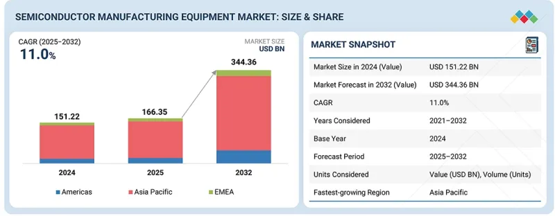
全球半导体製造设备市场预计将从 2025 年的 1,663.5 亿美元成长到 2032 年的 3,443.6 亿美元,复合年增长率为 11.0%。
汽车半导体产业的快速成长正成为2025年半导体製造设备市场的主要驱动力。随着汽车产业向电气化、自动驾驶、先进连接和软体定义架构发展,对包括微控制器、电源管理积体电路 (PMIC)、感测器和高级驾驶辅助系统 (ADAS) 处理器在内的高可靠性半导体组件的需求持续呈指数级增长。
| 调查范围 | |
|---|---|
| 调查期 | 2021-2032 |
| 基准年 | 2024 |
| 预测期 | 2025-2032 |
| 单元 | 10亿美元 |
| 部分 | 製造流程、最终用户、前端设备、后端设备、区域 |
| 目标区域 | 北美、欧洲、亚太地区及其他地区 |
电动车的快速普及以及每辆车半导体含量的不断提高,显着提升了对牵引逆变器、电池管理系统、电力电子设备、感测模组、ADAS平台等的高级晶片的需求。汽车製造商和一级供应商正在扩大晶圆厂产能并升级现有生产线,以生产车规级半导体,这直接推动了对微影术、沉积、蚀刻、计量和检测工具等关键设备的投资。鑑于汽车应用对性能、可靠性和可追溯性的严格要求,该领域尤其註重精密製造和严格的品管,这使得拥有车规级工具的半导体製造设备供应商受益匪浅。
“预计在预测期内,OSAT公司将实现最高的复合年增长率。”
由于OSAT公司处于行业快速向先进封装和高密度测试需求转型的核心地位,预计在预测期内,OSAT公司将实现最高的复合年增长率。随着晶片设计不断发展以支援人工智慧/机器学习、高效能运算、5G、自动驾驶和异质整合等应用,对先进后端製程(例如2.5D/3D封装、扇出晶圆层次电子构装、系统级封装(SiP)和高效能自动化测试设备(ATE))的需求持续激增。
无厂半导体公司越来越多地将组装和测试流程外包,以降低成本并加快产品上市速度,这迫使外包半导体组装测试与测试(OSAT)厂商扩大产能并采用先进设备。此外,日益复杂的几何尺寸、晶片级架构的普及以及对主导性能的日益重视,都显着推动了OSAT厂商的投资。这些因素使得OSAT厂商成为半导体製造设备市场中终端用户成长最快的细分领域。
“2024年,检测设备将引领半导体后端设备市场。”
测试设备在半导体后端设备市场中占据最大份额,因为每件半导体装置在出厂前都必须经过多道测试工序,以确保其功能准确性、性能可靠性和无缺陷运作。由于I/O数量增加、晶片尺寸缩小、晶片组架构以及先进封装形式的出现,晶片复杂性日益增加,这也显着提高了对全面的电气测试、功能测试、老化测试和系统级测试的需求。
此外,人工智慧加速器、汽车电子产品、工业自动化和5G等应用的兴起对可靠性和安全性提出了极高的要求,进一步提高了检测的强度和范围。随着装置故障成本的急剧上升,严格的检测已成为半导体製造商不可或缺的流程。因此,OSAT(外包半导体封装测试)厂商、IDM(集成器件制造商)和无厂半导体公司不断投资于先进的自动化测试设备(ATE)、探针系统和检测技术,从而巩固了检测设备在半导体后端设备市场的主导地位。
本报告对全球半导体製造设备市场进行了分析,提供了关键驱动因素和限制因素、竞争格局和未来趋势的资讯。
目录
第一章 引言
第二章执行摘要
第三章 主要发现
- 半导体製造设备市场对企业而言极具吸引力的机会
- 半导体製造设备市场:依最终用户划分
- 半导体製造设备市场:依前端设备
- 按地区分類的半导体製造设备市场
第四章 市场概览
- 介绍
- 市场动态
- 司机
- 抑制因素
- 机会
- 任务
- 未满足的需求和閒置频段
- 相互关联的市场与跨产业机会
- 一级/二级/三级公司的策略性倡议
第五章 产业趋势
- 波特五力分析
- 总体经济指标
- 介绍
- GDP趋势与预测
- 全球晶圆代工厂产业趋势
- 全球IDM产业趋势
- 全球OSAT产业趋势
- 价值链分析
- 生态系分析
- 定价分析
- 主要企业提供的前端微影术设备平均售价趋势(按类型划分)(2021-2024 年)
- 按地区分類的标准微影术设备平均售价趋势(2021-2024 年)
- 贸易分析
- 进口方案(HS编码848620)
- 出口方案(HS编码848620)
- 重大会议和活动(2025-2026)
- 影响客户业务的趋势/颠覆性因素
- 投资和资金筹措方案
- 案例研究分析
- 2025年美国关税对半导体製造设备市场的影响
- 介绍
- 主要关税税率
- 价格影响分析
- 对国家的影响
- 最终用户影响
第六章:技术进步、人工智慧的影响、专利、创新与未来应用
- 主要新技术
- 极紫外线(EUV)微影术
- 晶圆键合技术
- 互补技术
- 技术/产品蓝图
- 专利分析
- 人工智慧/生成式人工智慧对半导体製造设备市场的影响
- 主要应用案例和市场潜力
- 半导体製造设备市场的OEM最佳实践
- 半导体製造设备市场人工智慧应用案例研究
- 相互关联的生态系统及其对市场公司的影响
- 客户对采用人工智慧/生成式人工智慧整合半导体製造设备的准备情况
第七章 区域情势与永续性倡议
- 地方法规和合规性
- 监管机构、政府机构和其他组织
- 业界标准
- 对永续性的承诺
- 监管政策对永续性努力的影响
- 认证、标籤和环境标准
第八章:顾客状况与购买行为
- 决策流程
- 采购过程中的关键相关利益者及其评估标准
- 采购过程中的关键相关利益者
- 采购标准
- 招募障碍和内部挑战
- 各类终端用户的未满足需求
- 市场盈利
第九章 半导体製造设备中晶圆类型的概述
- 介绍
- 硅(SI)
- 碳化硅(SIC)
- 氮化镓(GAN)
- 砷化镓(GAAS)
- 其他晶圆类型
第十章:半导体製造设备的最终产品
- 介绍
- 记忆
- 逻辑装置
- MPU
- CPU
- GPU
- DSP
- 其他的
- 分立元件
- 类比IC
- 其他最终产品
第十一章:半导体製造设备中的各种积体电路尺寸
- 介绍
- 2D IC
- 2.5D IC
- 3D IC
第十二章:半导体製造设备加工的晶圆尺寸
- 介绍
- 150毫米或更小
- 200毫米
- 300毫米
第十三章 半导体製造设备市场(依製造流程划分)
- 介绍
- 预处理
- 后处理
- 其他流程
第十四章 半导体製造设备市场(依前端设备)
- 介绍
- 微影术设备
- 薄膜成型设备
- 晶圆表面处理设备
- 晶圆清洗设备
- 测量和检测设备
- 其他前端设备
第十五章 半导体製造设备市场(后端设备划分)
- 介绍
- 包装
- 切丁
- 黏合
- 晶圆检测/积体电路检测
第十六章 半导体製造设备市场(依最终用户划分)
- 介绍
- 晶圆代工厂
- IDMS
- OSAT公司
- 其他最终用户
第十七章 半导体製造设备市场(依地区划分)
- 介绍
- 美洲
- 美国
- 其他美洲
- 亚太地区
- 中国
- 日本
- 韩国
- 台湾
- 印度
- 亚太其他地区
- 欧洲、中东和非洲
- 欧洲
- 中东和非洲
第十八章 竞争格局
- 概述
- 主要参与企业的策略/优势(2024-2025)
- 收入分析(2020-2024)
- 市占率分析(2024 年)
- 公司估值和财务指标
- 产品对比
- 企业评估矩阵:主要企业(2024)
- 公司评估矩阵:Start-Ups/中小企业(2024 年)
- 竞争场景
第十九章:公司简介
- 介绍
- 主要企业
- APPLIED MATERIALS, INC.
- ASML
- TOKYO ELECTRON LIMITED
- LAM RESEARCH CORPORATION
- KLA CORPORATION
- SCREEN HOLDINGS CO., LTD.
- TERADYNE INC.
- ZEISS GROUP
- ADVANTEST CORPORATION
- HITACHI HIGH-TECH CORPORATION
- PLASMA-THERM
- 其他公司
- ASM INTERNATIONAL
- EV GROUP(EVG)
- ONTO INNOVATION
- NORDSON CORPORATION
- ADT-ADVANCED DICING TECHNOLOGIES
- BENEQ
- CVD EQUIPMENT CORPORATION
- EUGENE TECHNOLOGY CO. LTD.
- NIKON CORPORATION
- SEMICONDUCTOR EQUIPMENT CORP.
- SENTECH INSTRUMENTS GMBH
- CANON INC.
- KOKUSAI ELECTRIC CORPORATION
- SEMES
- FORMFACTOR
- 最终用户
- FOUNDRIES
- IDM FIRMS
- OSAT COMPANIES
第20章调查方法
第21章附录
The global semiconductor manufacturing equipment market is projected to grow from USD 166.35 billion in 2025 to USD 344.36 billion by 2032, at a CAGR of 11.0%. The rapid acceleration of the automotive semiconductor sector is emerging as a major driver of the semiconductor manufacturing equipment market in 2025. As the automotive industry transitions toward electrification, autonomous driving, enhanced connectivity, and software-defined architectures, demand for high-reliability semiconductor components, including microcontrollers, power-management ICs, sensors, and ADAS processors, continues to rise sharply.
| Scope of the Report | |
|---|---|
| Years Considered for the Study | 2021-2032 |
| Base Year | 2024 |
| Forecast Period | 2025-2032 |
| Units Considered | Value (USD Billion) |
| Segments | By Manufacturing Phase, End User, Front-end Equipment, Back-end Equipment and Region |
| Regions covered | North America, Europe, APAC, RoW |
The rapid shift toward EVs and higher semiconductor content per vehicle is substantially increasing demand for advanced chips used in traction inverters, battery-management systems, power electronics, sensing modules, and ADAS platforms. Automakers and tier-one suppliers are expanding fab capacity and upgrading existing lines to produce automotive-grade semiconductors, directly boosting investments in critical equipment such as lithography, deposition, etch, metrology, and inspection tools. Given the stringent performance, reliability, and traceability requirements in automotive applications, the segment places strong emphasis on precision manufacturing and robust quality control, benefiting semiconductor manufacturing equipment suppliers with automotive-qualified toolsets.
"OSAT Companies to Record Highest CAGR During Forecast Period"
OSAT companies are expected to record the highest CAGR during the forecast period because they are at the center of the industry's rapid shift toward advanced packaging and high-density testing requirements. As chip designs evolve to support AI/ML, HPC, 5G, automotive autonomy, and heterogeneous integration, the demand for sophisticated backend processes such as 2.5D/3D packaging, fan-out wafer-level packaging, system-in-package (SiP), and high-performance automated test equipment continues to surge.
Fabless companies are increasingly outsourcing assembly and testing to reduce costs and accelerate time-to-market, prompting OSATs to expand their capacity and adopt more advanced equipment. Furthermore, increased miniaturization, the adoption of chiplet-based architectures, and the transition toward packaging-driven performance improvements are significantly boosting OSAT investments. Collectively, these factors position OSAT companies as the fastest-growing segment in the semiconductor manufacturing equipment market based on end users.
"Testing Equipment Led Semiconductor Manufacturing Back-end Equipment Market in 2024"
Testing equipment holds the largest share of the back-end semiconductor manufacturing equipment market because every semiconductor device must undergo multiple mandatory test stages to ensure functional accuracy, performance reliability, and defect-free operation before shipment. As chips become more complex, with higher I/O counts, smaller geometries, chiplet architectures, and advanced packaging formats, the need for comprehensive electrical, functional, burn-in, and system-level testing increases significantly.
Moreover, the rise of applications such as AI accelerators, automotive electronics, industrial automation, and 5G requires extremely high reliability and safety standards, further increasing the intensity and coverage requirements of testing. The cost of device failure has risen sharply, making robust testing a non-negotiable step for semiconductor manufacturers. As a result, OSATs, IDMs, and fabless companies consistently invest in advanced automated test equipment (ATE), probing systems, and inspection technologies, thereby solidifying the leading position of testing equipment in the back-end semiconductor manufacturing equipment market.
"China to Dominate Asia Pacific Semiconductor Manufacturing Equipment Market throughout Forecast Period"
China holds the largest share of the semiconductor manufacturing equipment market due to its aggressive national push to expand domestic semiconductor production capacity and reduce dependence on foreign chip suppliers. The country has been investing heavily in new fabs, equipment procurement, and advanced manufacturing infrastructure as part of government-led initiatives, such as "Made in China 2025" and successive Five-year Plans, which prioritize semiconductor self-sufficiency.
China also hosts one of the world's fastest-growing ecosystems of foundries, memory manufacturers, and OSAT companies, such as JCET and Tongfu Microelectronics, driving continuous equipment purchases for capacity expansion and technology upgrades. Additionally, supply-chain localization efforts, coupled with increased government subsidies, tax incentives, and capital investments, have significantly boosted demand for equipment across lithography, etch, deposition, and backend packaging segments.
Breakdown of Primaries
Various executives from key organizations operating in the semiconductor manufacturing equipment market were interviewed in-depth, including CEOs, marketing directors, and innovation and technology directors.
- By Company Type: Tier 1 - 25%, Tier 2 - 35%, and Tier 3 - 40%
- By Designation: C-level Executives - 40%, Directors - 30%, and Others - 30%
- By Region: Asia Pacific - 45%, Americas - 35%, EMEA - 20%
The semiconductor manufacturing equipment market is dominated by globally established players, such as
Applied Materials, Inc. (US), ASML (Netherlands), Tokyo Electron Limited (Japan), LAM RESEARCH CORPORATION (US), KLA Corporation (US), SCREEN Holdings Co., Ltd. (Japan), Teradyne Inc. (US), ADVANTEST CORPORATION (Japan), Hitachi High-Tech Corporation (Japan), Plasma-Therm (US), ASM International N.V. (Netherlands), EV Group (EVG) (Austria), Onto Innovation (US), Nordson Corporation (US), ADT - Advanced Dicing Technologies (Israel), Beneq (Finland), CVD Equipment Corporation (US), Eugenus, Inc. (South Korea), Nikon Corporation (Japan), Semiconductor Equipment Corp. (US), SENTECH Instruments GmbH (Germany), Canon Inc. (Japan), KOKUSAI ELECTRIC CORPORATION (Japan), SEMES (South Korea), and FormFactor (US). The study includes an in-depth competitive analysis of these key players in the semiconductor manufacturing equipment market, with their company profiles, recent developments, and key market strategies.
Study Coverage
The report segments the semiconductor manufacturing equipment market by manufacturing phase, including front-end equipment and back-end equipment, end user, and region. The report also examines the key drivers, restraints, opportunities, and challenges influencing the market. It provides a detailed view of the market across three main regions: the Americas, Asia Pacific, and EMEA. The report includes a value chain analysis of the key players and their competitive analysis of the semiconductor manufacturing equipment ecosystem.
Key benefits of buying the report are as follows:
- Analysis of key drivers (rising miniaturization and advanced node adoption), restraints (high capital and operational costs), opportunities (rising adoption of advanced packaging technologies), and challenges (stringent regulatory compliance) influencing the growth of the semiconductor manufacturing equipment market
- Products/Solution/Service Development/Innovation: Detailed insights into upcoming technologies, research, and development activities in the semiconductor manufacturing equipment market
- Market Development: Comprehensive information about lucrative markets, provided by analyzing the semiconductor manufacturing equipment market across varied regions
- Market Diversification: Exhaustive information about new semiconductor manufacturing equipment in untapped geographies, recent developments, and investments in the semiconductor manufacturing equipment market
- Competitive Assessment: In-depth assessment of market shares and growth strategies and offerings of leading players, such as Applied Materials, Inc. (US), ASML (Netherlands), LAM RESEARCH CORPORATION (US), Tokyo Electron Limited (Japan), and KLA Corporation (US)
TABLE OF CONTENTS
1 INTRODUCTION
- 1.1 STUDY OBJECTIVES
- 1.2 MARKET DEFINITION
- 1.3 STUDY SCOPE
- 1.3.1 MARKETS COVERED AND REGIONAL SCOPE
- 1.3.2 INCLUSIONS AND EXCLUSIONS
- 1.3.3 YEARS CONSIDERED
- 1.4 CURRENCY CONSIDERED
- 1.5 UNIT CONSIDERED
- 1.6 LIMITATIONS
- 1.7 STAKEHOLDERS
- 1.8 SUMMARY OF CHANGES
2 EXECUTIVE SUMMARY
- 2.1 MARKET HIGHLIGHTS AND KEY INSIGHTS
- 2.2 KEY MARKET PARTICIPANTS: MAPPING OF STRATEGIC DEVELOPMENTS
- 2.3 DISRUPTIVE TRENDS IN SEMICONDUCTOR MANUFACTURING EQUIPMENT MARKET
- 2.4 HIGH-GROWTH SEGMENTS
- 2.5 SNAPSHOT: GLOBAL MARKET SIZE, GROWTH RATE, AND FORECAST
3 PREMIUM INSIGHTS
- 3.1 ATTRACTIVE OPPORTUNITIES FOR PLAYERS IN SEMICONDUCTOR MANUFACTURING EQUIPMENT MARKET
- 3.2 SEMICONDUCTOR MANUFACTURING EQUIPMENT MARKET, BY END USER
- 3.3 SEMICONDUCTOR MANUFACTURING EQUIPMENT MARKET, BY FRONT-END EQUIPMENT
- 3.4 SEMICONDUCTOR MANUFACTURING EQUIPMENT MARKET, BY REGION
4 MARKET OVERVIEW
- 4.1 INTRODUCTION
- 4.2 MARKET DYNAMICS
- 4.2.1 DRIVERS
- 4.2.1.1 Increasing miniaturization and advanced node adoption
- 4.2.1.2 Rising autonomous vehicle adoption and digitalization
- 4.2.1.3 Rapid expansion of semiconductor fabrication capacity
- 4.2.1.4 Proliferation of AI, HPC, and data-centric workloads
- 4.2.2 RESTRAINTS
- 4.2.2.1 High capital and operational costs
- 4.2.2.2 Rising complexity of semiconductor manufacturing processes
- 4.2.3 OPPORTUNITIES
- 4.2.3.1 Mounting adoption of advanced packaging technologies
- 4.2.3.2 Government-led initiatives to strengthen semiconductor manufacturing
- 4.2.4 CHALLENGES
- 4.2.4.1 Complexities associated with transitioning to smaller geometries and higher transistor densities
- 4.2.4.2 Rising implementation of stringent environmental norms
- 4.2.1 DRIVERS
- 4.3 UNMET NEEDS AND WHITE SPACES
- 4.4 INTERCONNECTED MARKETS AND CROSS-SECTOR OPPORTUNITIES
- 4.5 STRATEGIC MOVES BY TIER 1/2/3 PLAYERS
5 INDUSTRY TRENDS
- 5.1 PORTER'S FIVE FORCES ANALYSIS
- 5.1.1 INTENSITY OF COMPETITIVE RIVALRY
- 5.1.2 BARGAINING POWER OF SUPPLIERS
- 5.1.3 BARGAINING POWER OF BUYERS
- 5.1.4 THREAT OF SUBSTITUTES
- 5.1.5 THREAT OF NEW ENTRANTS
- 5.2 MACROECONOMICS INDICATORS
- 5.2.1 INTRODUCTION
- 5.2.2 GDP TRENDS AND FORECAST
- 5.2.3 TRENDS IN GLOBAL FOUNDRY INDUSTRY
- 5.2.4 TRENDS IN GLOBAL IDM INDUSTRY
- 5.2.5 TRENDS IN GLOBAL OSAT INDUSTRY
- 5.3 VALUE CHAIN ANALYSIS
- 5.4 ECOSYSTEM ANALYSIS
- 5.5 PRICING ANALYSIS
- 5.5.1 AVERAGE SELLING PRICE TREND OF FRONT-END LITHOGRAPHY EQUIPMENT OFFERED BY KEY PLAYERS, BY TYPE, 2021-2024
- 5.5.2 AVERAGE SELLING PRICE TREND OF STANDARD LITHOGRAPHY EQUIPMENT, BY REGION, 2021-2024
- 5.6 TRADE ANALYSIS
- 5.6.1 IMPORT SCENARIO (HS CODE 848620)
- 5.6.2 EXPORT SCENARIO (HS CODE 848620)
- 5.7 KEY CONFERENCES AND EVENTS, 2025-2026
- 5.8 TRENDS/DISRUPTIONS IMPACTING CUSTOMER BUSINESS
- 5.9 INVESTMENT AND FUNDING SCENARIO
- 5.10 CASE STUDY ANALYSIS
- 5.10.1 HCL AND FOXCONN COLLABORATE TO ESTABLISH OSAT FACILITY IN INDIA TO NAVIGATE REGULATORY COMPLEXITIES
- 5.10.2 SYNOVA SA IMPLEMENTS LASER MICROJET TECHNOLOGY TO ACHIEVE PRECISE AND HIGH-QUALITY WAFER DICING AND DIE SINGULATION
- 5.10.3 INTEL SECURES ASML'S HIGH-NA EUV MACHINES TO PRODUCE ADVANCED CHIPS WITH GREATER PRECISION AND EFFICIENCY
- 5.11 IMPACT OF 2025 US TARIFF ON SEMICONDUCTOR MANUFACTURING EQUIPMENT MARKET
- 5.11.1 INTRODUCTION
- 5.11.2 KEY TARIFF RATES
- 5.11.3 PRICE IMPACT ANALYSIS
- 5.11.4 IMPACT ON COUNTRIES/REGIONS
- 5.11.4.1 US
- 5.11.4.2 Europe
- 5.11.4.3 Asia Pacific
- 5.11.5 IMPACT ON END USERS
6 TECHNOLOGICAL ADVANCEMENTS, AI-DRIVEN IMPACTS, PATENTS, INNOVATIONS, AND FUTURE APPLICATIONS
- 6.1 KEY EMERGING TECHNOLOGIES
- 6.1.1 EXTREME ULTRAVIOLET (EUV) LITHOGRAPHY
- 6.1.2 WAFER BONDING
- 6.2 COMPLEMENTARY TECHNOLOGIES
- 6.2.1 FLIP CHIP
- 6.3 TECHNOLOGY/PRODUCT ROADMAP
- 6.4 PATENT ANALYSIS
- 6.5 IMPACT OF AI/GEN AI ON SEMICONDUCTOR MANUFACTURING EQUIPMENT MARKET
- 6.5.1 TOP USE CASES AND MARKET POTENTIAL
- 6.5.2 BEST PRACTICES FOLLOWED BY OEMS IN SEMICONDUCTOR MANUFACTURING EQUIPMENT MARKET
- 6.5.3 CASE STUDIES RELATED TO AI IMPLEMENTATION IN SEMICONDUCTOR MANUFACTURING EQUIPMENT MARKET
- 6.5.4 INTERCONNECTED ECOSYSTEM AND IMPACT ON MARKET PLAYERS
- 6.5.5 CLIENTS' READINESS TO ADOPT AI/GEN AI-INTEGRATED SEMICONDUCTOR MANUFACTURING EQUIPMENT
7 REGIONAL LANDSCAPE AND SUSTAINABILITY INITIATIVES
- 7.1 REGIONAL REGULATIONS AND COMPLIANCE
- 7.1.1 REGULATORY BODIES, GOVERNMENT AGENCIES, AND OTHER ORGANIZATIONS
- 7.1.2 INDUSTRY STANDARDS
- 7.2 SUSTAINABILITY INITIATIVES
- 7.2.1 CARBON IMPACT AND ECO-APPLICATION FOR SEMICONDUCTOR MANUFACTURING EQUIPMENT
- 7.3 IMPACT OF REGULATORY POLICIES ON SUSTAINABILITY INITIATIVES
- 7.4 CERTIFICATIONS, LABELING, AND ECO-STANDARDS
8 CUSTOMER LANDSCAPE AND BUYER BEHAVIOR
- 8.1 DECISION-MAKING PROCESS
- 8.2 KEY STAKEHOLDERS INVOLVED IN BUYING PROCESS AND THEIR EVALUATION CRITERIA
- 8.2.1 KEY STAKEHOLDERS IN BUYING PROCESS
- 8.2.2 BUYING CRITERIA
- 8.3 ADOPTION BARRIERS AND INTERNAL CHALLENGES
- 8.4 UNMET NEEDS OF VARIOUS END USERS
- 8.5 MARKET PROFITABILITY
9 OVERVIEW OF WAFER TYPES IN SEMICONDUCTOR MANUFACTURING EQUIPMENT
- 9.1 INTRODUCTION
- 9.2 SILICON (SI)
- 9.3 SILICON CARBIDE (SIC)
- 9.4 GALLIUM NITRIDE (GAN)
- 9.5 GALLIUM ARSENIDE (GAAS)
- 9.6 OTHER WAFER TYPES
10 END PRODUCTS OF SEMICONDUCTOR MANUFACTURING EQUIPMENT
- 10.1 INTRODUCTION
- 10.2 MEMORY
- 10.3 LOGIC DEVICES
- 10.3.1 MPU
- 10.3.2 CPU
- 10.3.3 GPU
- 10.3.4 DSP
- 10.3.5 OTHERS
- 10.4 DISCRETE DEVICES
- 10.5 ANALOG ICS
- 10.6 OTHER END PRODUCTS
11 VARIED IC DIMENSIONS WITHIN SEMICONDUCTOR MANUFACTURING EQUIPMENT
- 11.1 INTRODUCTION
- 11.2 2D ICS
- 11.3 2.5D ICS
- 11.4 3D ICS
12 WAFER SIZES PROCESSED BY SEMICONDUCTOR MANUFACTURING EQUIPMENT
- 12.1 INTRODUCTION
- 12.2 <=150 MM
- 12.3 200 MM
- 12.4 300 MM
13 SEMICONDUCTOR MANUFACTURING EQUIPMENT MARKET, BY MANUFACTURING PHASE
- 13.1 INTRODUCTION
- 13.2 FRONT-END
- 13.2.1 EMPHASIS ON ENERGY EFFICIENCY, DEFECT REDUCTION, AND SUSTAINABILITY TO FOSTER SEGMENTAL GROWTH
- 13.3 BACK-END
- 13.3.1 ADVANCES IN WAFER-LEVEL FAN-OUT PACKAGING AND FOCUS ON TEST OPTIMIZATION TO EXPEDITE SEGMENTAL GROWTH
- 13.4 OTHER PHASES
14 SEMICONDUCTOR MANUFACTURING EQUIPMENT MARKET, BY FRONT-END EQUIPMENT
- 14.1 INTRODUCTION
- 14.2 LITHOGRAPHY EQUIPMENT
- 14.2.1 FOCUS ON OPTICAL PRECISION AND OVERLAY ACCURACY TO SUPPORT NEXT-GENERATION FABRICATION TO DRIVE MARKET
- 14.2.2 PHOTOLITHOGRAPHY
- 14.2.2.1 Deep ultraviolet (DUV)
- 14.2.2.2 Extreme ultraviolet (EUV)
- 14.2.3 ELECTRON BEAM LITHOGRAPHY
- 14.2.4 ION BEAM LITHOGRAPHY
- 14.2.5 NANOIMPRINT LITHOGRAPHY
- 14.2.6 OTHER LITHOGRAPHY EQUIPMENT
- 14.3 DEPOSITION EQUIPMENT
- 14.3.1 EVOLUTION OF DEVICE SCALING AND 3D INTEGRATION TO CONTRIBUTE TO SEGMENTAL GROWTH
- 14.3.2 CVD
- 14.3.3 PVD
- 14.4 WAFER SURFACE CONDITIONING EQUIPMENT
- 14.4.1 ETCHING EQUIPMENT
- 14.4.1.1 Ability to achieve precise dimensional control, high aspect ratios, and minimal defect generation to boost segmental growth
- 14.4.2 CMP EQUIPMENT
- 14.4.2.1 Use to enable accurate photolithography alignment, reliable interconnect formation, and optimal device performance to drive market
- 14.4.1 ETCHING EQUIPMENT
- 14.5 WAFER CLEANING EQUIPMENT
- 14.5.1 FOCUS ON ENSURING DEFECT-FREE DEVICE FABRICATION TO ACCELERATE SEGMENTAL GROWTH
- 14.6 METROLOGY & INSPECTION EQUIPMENT
- 14.6.1 ABILITY TO HELP MEET DESIGN AND RELIABILITY SPECIFICATIONS TO BOLSTER SEGMENTAL GROWTH
- 14.6.2 WAFER/SUBSTRATE INSPECTION
- 14.6.3 EPITAXIAL LAYER METROLOGY
- 14.6.4 IN-LINE PROCESS METROLOGY
- 14.6.5 ELECTRICAL & WAFER TEST METROLOGY
- 14.6.6 DEFECT REVIEW & CLASSIFICATION
- 14.7 OTHER FRONT-END EQUIPMENT
15 SEMICONDUCTOR MANUFACTURING EQUIPMENT MARKET, BY BACK-END EQUIPMENT
- 15.1 INTRODUCTION
- 15.2 PACKAGING
- 15.2.1 EMPHASIS ON HETEROGENEOUS INTEGRATION AND CHIPLET-BASED ARCHITECTURES IN SEMICONDUCTOR DEVICES TO FUEL SEGMENTAL GROWTH
- 15.3 DICING
- 15.3.1 MOUNTING DEMAND FOR HIGH-PRECISION SEMICONDUCTOR DEVICES TO SUPPORT SEGMENTAL GROWTH
- 15.3.1.1 Blade dicing
- 15.3.1.2 Laser dicing
- 15.3.1.3 Stealth dicing
- 15.3.1.4 Scribing & breaking tools
- 15.3.1 MOUNTING DEMAND FOR HIGH-PRECISION SEMICONDUCTOR DEVICES TO SUPPORT SEGMENTAL GROWTH
- 15.4 BONDING
- 15.4.1 DEVELOPMENT OF ADVANCED SEMICONDUCTOR PACKAGING TECHNOLOGY TO CONTRIBUTE TO SEGMENTAL GROWTH
- 15.4.2 DIE ATTACH
- 15.4.3 WIRE BONDING
- 15.4.4 FLIP-CHIP BONDING
- 15.4.5 HYBRID BONDING
- 15.5 WAFER TESTING/IC TESTING
- 15.5.1 ABILITY TO ENSURE FUNCTIONALITY, RELIABILITY, AND PERFORMANCE OF SEMICONDUCTOR DEVICES TO FOSTER SEGMENTAL GROWTH
16 SEMICONDUCTOR MANUFACTURING EQUIPMENT MARKET, BY END USER
- 16.1 INTRODUCTION
- 16.2 FOUNDRIES
- 16.2.1 CAPACITY EXPANSION AND INVESTMENT IN SMALL PROCESS NODES TO BOLSTER SEGMENTAL GROWTH
- 16.3 IDMS
- 16.3.1 ADOPTION OF ADVANCED PACKAGING TECHNIQUES TO CONTRIBUTE TO SEGMENTAL GROWTH
- 16.4 OSAT COMPANIES
- 16.4.1 FOCUS ON ADVANCED ASSEMBLY, BONDING, AND INSPECTION OF SEMICONDUCTOR DEVICES TO FOSTER SEGMENTAL GROWTH
- 16.5 OTHER END USERS
17 SEMICONDUCTOR MANUFACTURING EQUIPMENT MARKET, BY REGION
- 17.1 INTRODUCTION
- 17.2 AMERICAS
- 17.2.1 US
- 17.2.1.1 Surge in fab construction to accelerate market growth
- 17.2.2 REST OF AMERICAS
- 17.2.1 US
- 17.3 ASIA PACIFIC
- 17.3.1 CHINA
- 17.3.1.1 Government initiatives to strengthen semiconductor equipment supply chain to boost market growth
- 17.3.2 JAPAN
- 17.3.2.1 High expertise in precision engineering and materials science to augment market growth
- 17.3.3 SOUTH KOREA
- 17.3.3.1 Escalating memory chip production to contribute to market growth
- 17.3.4 TAIWAN
- 17.3.4.1 Increasing investment in cleanroom equipment to foster market growth
- 17.3.5 INDIA
- 17.3.5.1 Evolving semiconductor supply-chain ecosystem to accelerate market growth
- 17.3.6 REST OF ASIA PACIFIC
- 17.3.1 CHINA
- 17.4 EMEA
- 17.4.1 EUROPE
- 17.4.1.1 Increasing investment in semiconductor facility construction to fuel market growth
- 17.4.2 MIDDLE EAST & AFRICA
- 17.4.2.1 Strong focus on localizing advanced manufacturing capabilities to bolster market growth
- 17.4.1 EUROPE
18 COMPETITIVE LANDSCAPE
- 18.1 OVERVIEW
- 18.2 KEY PLAYER STRATEGIES/RIGHT TO WIN, 2024-2025
- 18.3 REVENUE ANALYSIS, 2020-2024
- 18.4 MARKET SHARE ANALYSIS, 2024
- 18.5 COMPANY VALUATION AND FINANCIAL METRICS
- 18.6 PRODUCT COMPARISON
- 18.7 COMPANY EVALUATION MATRIX: KEY PLAYERS, 2024
- 18.7.1 STARS
- 18.7.2 EMERGING LEADERS
- 18.7.3 PERVASIVE PLAYERS
- 18.7.4 PARTICIPANTS
- 18.7.5 COMPANY FOOTPRINT: KEY PLAYERS, 2024
- 18.7.5.1 Company footprint
- 18.7.5.2 Region footprint
- 18.7.5.3 Manufacturing phase footprint
- 18.7.5.4 Front-end equipment footprint
- 18.7.5.5 Back-end equipment footprint
- 18.7.5.6 End user footprint
- 18.8 COMPANY EVALUATION MATRIX: STARTUPS/SMES, 2024
- 18.8.1 PROGRESSIVE COMPANIES
- 18.8.2 RESPONSIVE COMPANIES
- 18.8.3 DYNAMIC COMPANIES
- 18.8.4 STARTING BLOCKS
- 18.8.5 COMPETITIVE BENCHMARKING: STARTUPS/SMES, 2024
- 18.8.5.1 Detailed list of key startups/SMEs
- 18.8.5.2 Competitive benchmarking of key startups/SMEs
- 18.9 COMPETITIVE SCENARIO
- 18.9.1 PRODUCT LAUNCHES
- 18.9.2 DEALS
19 COMPANY PROFILES
- 19.1 INTRODUCTION
- 19.2 KEY PLAYERS
- 19.2.1 APPLIED MATERIALS, INC.
- 19.2.1.1 Business overview
- 19.2.1.2 Products/Solutions/Services offered
- 19.2.1.3 Recent developments
- 19.2.1.3.1 Product launches
- 19.2.1.3.2 Deals
- 19.2.1.3.3 Expansions
- 19.2.1.4 MnM view
- 19.2.1.4.1 Key strengths/Right to win
- 19.2.1.4.2 Strategic choices
- 19.2.1.4.3 Weaknesses/Competitive threats
- 19.2.2 ASML
- 19.2.2.1 Business overview
- 19.2.2.2 Products/Solutions/Services offered
- 19.2.2.3 Recent developments
- 19.2.2.3.1 Product launches
- 19.2.2.3.2 Deals
- 19.2.2.4 MnM view
- 19.2.2.4.1 Key strengths/Right to win
- 19.2.2.4.2 Strategic choices
- 19.2.2.4.3 Weaknesses/Competitive threats
- 19.2.3 TOKYO ELECTRON LIMITED
- 19.2.3.1 Business overview
- 19.2.3.2 Products/Solutions/Services offered
- 19.2.3.3 Recent developments
- 19.2.3.3.1 Product launches
- 19.2.3.3.2 Deals
- 19.2.3.4 MnM view
- 19.2.3.4.1 Key strengths/Right to win
- 19.2.3.4.2 Strategic choices
- 19.2.3.4.3 Weaknesses/Competitive threats
- 19.2.4 LAM RESEARCH CORPORATION
- 19.2.4.1 Business overview
- 19.2.4.2 Products/Solutions/Services offered
- 19.2.4.3 Recent developments
- 19.2.4.3.1 Product launches
- 19.2.4.3.2 Deals
- 19.2.4.3.3 Expansions
- 19.2.4.4 MnM view
- 19.2.4.4.1 Key strengths/Right to win
- 19.2.4.4.2 Strategic choices
- 19.2.4.4.3 Weaknesses/Competitive threats
- 19.2.5 KLA CORPORATION
- 19.2.5.1 Business overview
- 19.2.5.2 Products/Solutions/Services offered
- 19.2.5.3 Recent developments
- 19.2.5.3.1 Product launches
- 19.2.5.3.2 Expansions
- 19.2.5.4 MnM view
- 19.2.5.4.1 Key strengths/Right to win
- 19.2.5.4.2 Strategic choices
- 19.2.5.4.3 Weaknesses/Competitive threats
- 19.2.6 SCREEN HOLDINGS CO., LTD.
- 19.2.6.1 Business overview
- 19.2.6.2 Products/Solutions/Services offered
- 19.2.6.3 Recent developments
- 19.2.6.3.1 Product launches
- 19.2.6.3.2 Deals
- 19.2.6.4 MnM view
- 19.2.6.4.1 Key strengths/Right to win
- 19.2.6.4.2 Strategic choices
- 19.2.6.4.3 Weaknesses/Competitive threats
- 19.2.7 TERADYNE INC.
- 19.2.7.1 Business overview
- 19.2.7.2 Products/Solutions/Services offered
- 19.2.7.3 Recent developments
- 19.2.7.3.1 Product launches
- 19.2.7.3.2 Deals
- 19.2.7.4 MnM view
- 19.2.7.4.1 Key strengths/Right to win
- 19.2.7.4.2 Strategic choices
- 19.2.7.4.3 Weaknesses/Competitive threats
- 19.2.8 ZEISS GROUP
- 19.2.8.1 Business overview
- 19.2.8.2 Products/Solutions/Services offered
- 19.2.8.3 Recent developments
- 19.2.8.3.1 Product launches
- 19.2.8.3.2 Deals
- 19.2.8.4 MnM view
- 19.2.8.4.1 Key strengths/Right to win
- 19.2.8.4.2 Strategic choices
- 19.2.8.4.3 Weaknesses/Competitive threats
- 19.2.9 ADVANTEST CORPORATION
- 19.2.9.1 Business overview
- 19.2.9.2 Products/Solutions/Services offered
- 19.2.9.3 Recent developments
- 19.2.9.3.1 Deals
- 19.2.9.4 MnM view
- 19.2.9.4.1 Key strengths/Right to win
- 19.2.9.4.2 Strategic choices
- 19.2.9.4.3 Weaknesses/Competitive threats
- 19.2.10 HITACHI HIGH-TECH CORPORATION
- 19.2.10.1 Business overview
- 19.2.10.2 Products/Solutions/Services offered
- 19.2.10.3 Recent developments
- 19.2.10.3.1 Product launches
- 19.2.10.3.2 Deals
- 19.2.10.4 MnM view
- 19.2.10.4.1 Key strengths/Right to win
- 19.2.10.4.2 Strategic choices
- 19.2.10.4.3 Weaknesses/Competitive threats
- 19.2.11 PLASMA-THERM
- 19.2.11.1 Business overview
- 19.2.11.2 Products/Solutions/Services offered
- 19.2.11.3 MnM view
- 19.2.11.3.1 Key strengths/Right to win
- 19.2.11.3.2 Strategic choices
- 19.2.11.3.3 Weaknesses/Competitive threats
- 19.2.1 APPLIED MATERIALS, INC.
- 19.3 OTHER PLAYERS
- 19.3.1 ASM INTERNATIONAL
- 19.3.2 EV GROUP (EVG)
- 19.3.3 ONTO INNOVATION
- 19.3.4 NORDSON CORPORATION
- 19.3.5 ADT - ADVANCED DICING TECHNOLOGIES
- 19.3.6 BENEQ
- 19.3.7 CVD EQUIPMENT CORPORATION
- 19.3.8 EUGENE TECHNOLOGY CO. LTD.
- 19.3.9 NIKON CORPORATION
- 19.3.10 SEMICONDUCTOR EQUIPMENT CORP.
- 19.3.11 SENTECH INSTRUMENTS GMBH
- 19.3.12 CANON INC.
- 19.3.13 KOKUSAI ELECTRIC CORPORATION
- 19.3.14 SEMES
- 19.3.15 FORMFACTOR
- 19.4 END USERS
- 19.4.1 FOUNDRIES
- 19.4.1.1 Taiwan Semiconductor Manufacturing Company Limited
- 19.4.1.2 Samsung
- 19.4.1.3 GlobalFoundries
- 19.4.1.4 SMIC
- 19.4.1.5 United Microelectronics Corporation
- 19.4.2 IDM FIRMS
- 19.4.2.1 Intel Corporation
- 19.4.2.2 Texas Instruments Incorporated
- 19.4.2.3 Infineon Technologies AG
- 19.4.3 OSAT COMPANIES
- 19.4.3.1 ASE Technology Holding Co., Ltd.
- 19.4.3.2 Amkor Technology
- 19.4.1 FOUNDRIES
20 RESEARCH METHODOLOGY
- 20.1 RESEARCH DATA
- 20.2 SECONDARY AND PRIMARY RESEARCH
- 20.2.1 SECONDARY DATA
- 20.2.1.1 List of key secondary sources
- 20.2.1.2 Key data from secondary sources
- 20.2.2 PRIMARY DATA
- 20.2.2.1 List of primary interview participants
- 20.2.2.2 Breakdown of primaries
- 20.2.2.3 Key data from primary sources
- 20.2.2.4 Key industry insights
- 20.2.1 SECONDARY DATA
- 20.3 MARKET SIZE ESTIMATION
- 20.3.1 BOTTOM-UP APPROACH
- 20.3.1.1 Approach to arrive at market size using bottom-up analysis (demand side)
- 20.3.2 TOP-DOWN APPROACH
- 20.3.2.1 Approach to arrive at market size using top-down analysis (supply side)
- 20.3.3 MARKET SIZE CALCULATION FOR BASE YEAR
- 20.3.1 BOTTOM-UP APPROACH
- 20.4 MARKET FORECAST APPROACH
- 20.4.1 SUPPLY SIDE
- 20.4.2 DEMAND SIDE
- 20.5 MARKET BREAKDOWN AND DATA TRIANGULATION
- 20.6 RESEARCH ASSUMPTIONS
- 20.7 RESEARCH LIMITATIONS
- 20.8 RISK ANALYSIS
21 APPENDIX
- 21.1 INSIGHTS FROM INDUSTRY EXPERTS
- 21.2 DISCUSSION GUIDE
- 21.3 KNOWLEDGESTORE: MARKETSANDMARKETS' SUBSCRIPTION PORTAL
- 21.4 CUSTOMIZATION OPTIONS
- 21.5 RELATED REPORTS
- 21.6 AUTHOR DETAILS
List of Tables
- TABLE 1 SEMICONDUCTOR MANUFACTURING EQUIPMENT MARKET: INCLUSIONS AND EXCLUSIONS
- TABLE 2 SEMICONDUCTOR MANUFACTURING EQUIPMENT MARKET: SUMMARY OF CHANGES
- TABLE 3 UNMET NEEDS AND WHITE SPACES
- TABLE 4 INTERCONNECTED MARKETS AND CROSS-SECTOR OPPORTUNITIES
- TABLE 5 STRATEGIC MOVES BY TIER 1/2/3 PLAYERS
- TABLE 6 IMPACT OF PORTER'S FIVE FORCES
- TABLE 7 ROLE OF COMPANIES IN SEMICONDUCTOR MANUFACTURING EQUIPMENT ECOSYSTEM
- TABLE 8 AVERAGE SELLING PRICE TREND OF FRONT-END LITHOGRAPHY EQUIPMENT OFFERED BY KEY PLAYERS, 2021-2024 (USD MILLION)
- TABLE 9 AVERAGE SELLING PRICE TREND OF STANDARD LITHOGRAPHY EQUIPMENT, BY REGION, 2021-2024 (USD MILLION)
- TABLE 10 IMPORT DATA FOR HS CODE 848620-COMPLIANT PRODUCTS, BY COUNTRY, 2020-2024 (USD MILLION)
- TABLE 11 EXPORT DATA FOR HS CODE 848620-COMPLIANT PRODUCTS, BY COUNTRY, 2020-2024 (USD MILLION)
- TABLE 12 LIST OF KEY CONFERENCES AND EVENTS, 2025-2026
- TABLE 13 US-ADJUSTED RECIPROCAL TARIFF RATES
- TABLE 14 TECHNOLOGY/PRODUCT ROADMAP
- TABLE 15 LIST OF MAJOR PATENTS, 2021-2024
- TABLE 16 TOP USE CASES AND MARKET POTENTIAL
- TABLE 17 BEST PRACTICES: COMPANIES IMPLEMENTING USE CASES
- TABLE 18 SEMICONDUCTOR MANUFACTURING EQUIPMENT MARKET: CASE STUDIES RELATED TO AI IMPLEMENTATION
- TABLE 19 INTERCONNECTED ECOSYSTEM AND IMPACT ON MARKET PLAYERS
- TABLE 20 AMERICAS: REGULATORY BODIES, GOVERNMENT AGENCIES, AND OTHER ORGANIZATIONS
- TABLE 21 EMEA: REGULATORY BODIES, GOVERNMENT AGENCIES, AND OTHER ORGANIZATIONS
- TABLE 22 ASIA PACIFIC: REGULATORY BODIES, GOVERNMENT AGENCIES, AND OTHER ORGANIZATIONS
- TABLE 23 INFLUENCE OF STAKEHOLDERS ON BUYING PROCESS FOR TOP THREE END USERS (%)
- TABLE 24 KEY BUYING CRITERIA FOR THREE END USERS
- TABLE 25 UNMET NEEDS OF END USERS IN SEMICONDUCTOR MANUFACTURING EQUIPMENT MARKET
- TABLE 26 SEMICONDUCTOR MANUFACTURING EQUIPMENT MARKET, BY MANUFACTURING PHASE, 2021-2024 (USD BILLION)
- TABLE 27 SEMICONDUCTOR MANUFACTURING EQUIPMENT MARKET, BY MANUFACTURING PHASE, 2025-2032 (USD BILLION)
- TABLE 28 FRONT-END: SEMICONDUCTOR MANUFACTURING EQUIPMENT MARKET, BY REGION, 2021-2024 (USD BILLION)
- TABLE 29 FRONT-END: SEMICONDUCTOR MANUFACTURING EQUIPMENT MARKET, BY REGION, 2025-2032 (USD BILLION)
- TABLE 30 FRONT-END: SEMICONDUCTOR MANUFACTURING EQUIPMENT MARKET IN AMERICAS, BY COUNTRY, 2021-2024 (USD MILLION)
- TABLE 31 FRONT-END: SEMICONDUCTOR MANUFACTURING EQUIPMENT MARKET IN AMERICAS, BY COUNTRY, 2025-2032 (USD MILLION)
- TABLE 32 FRONT-END: SEMICONDUCTOR MANUFACTURING EQUIPMENT MARKET IN ASIA PACIFIC, BY COUNTRY, 2021-2024 (USD MILLION)
- TABLE 33 FRONT-END: SEMICONDUCTOR MANUFACTURING EQUIPMENT MARKET IN ASIA PACIFIC, BY COUNTRY, 2025-2032 (USD MILLION)
- TABLE 34 FRONT-END: SEMICONDUCTOR MANUFACTURING EQUIPMENT MARKET IN EMEA, BY REGION, 2021-2024 (USD MILLION)
- TABLE 35 FRONT-END: SEMICONDUCTOR MANUFACTURING EQUIPMENT MARKET IN EMEA, BY REGION, 2025-2032 (USD MILLION)
- TABLE 36 BACK-END: SEMICONDUCTOR MANUFACTURING EQUIPMENT MARKET, BY REGION, 2021-2024 (USD BILLION)
- TABLE 37 BACK-END: SEMICONDUCTOR MANUFACTURING EQUIPMENT MARKET, BY REGION, 2025-2032 (USD BILLION)
- TABLE 38 BACK-END: SEMICONDUCTOR MANUFACTURING EQUIPMENT MARKET IN AMERICAS, BY COUNTRY, 2021-2024 (USD MILLION)
- TABLE 39 BACK-END: SEMICONDUCTOR MANUFACTURING EQUIPMENT MARKET IN AMERICAS, BY COUNTRY, 2025-2032 (USD MILLION)
- TABLE 40 BACK-END: SEMICONDUCTOR MANUFACTURING EQUIPMENT MARKET IN ASIA PACIFIC, BY COUNTRY, 2021-2024 (USD MILLION)
- TABLE 41 BACK-END: SEMICONDUCTOR MANUFACTURING EQUIPMENT MARKET IN ASIA PACIFIC, BY COUNTRY, 2025-2032 (USD MILLION)
- TABLE 42 BACK-END: SEMICONDUCTOR MANUFACTURING EQUIPMENT MARKET IN EMEA, BY REGION, 2021-2024 (USD MILLION)
- TABLE 43 BACK-END: SEMICONDUCTOR MANUFACTURING EQUIPMENT MARKET IN EMEA, BY REGION, 2025-2032 (USD MILLION)
- TABLE 44 OTHER PHASES: SEMICONDUCTOR MANUFACTURING EQUIPMENT MARKET, BY REGION, 2021-2024 (USD BILLION)
- TABLE 45 OTHER PHASES: SEMICONDUCTOR MANUFACTURING EQUIPMENT MARKET, BY REGION, 2025-2032 (USD BILLION)
- TABLE 46 OTHER PHASES: SEMICONDUCTOR MANUFACTURING EQUIPMENT MARKET IN AMERICAS, BY COUNTRY, 2021-2024 (USD MILLION)
- TABLE 47 OTHER PHASES: SEMICONDUCTOR MANUFACTURING EQUIPMENT MARKET IN AMERICAS, BY COUNTRY, 2025-2032 (USD MILLION)
- TABLE 48 OTHER PHASES: SEMICONDUCTOR MANUFACTURING EQUIPMENT MARKET IN ASIA PACIFIC, BY COUNTRY, 2021-2024 (USD MILLION)
- TABLE 49 OTHER PHASES: SEMICONDUCTOR MANUFACTURING EQUIPMENT MARKET IN ASIA PACIFIC, BY COUNTRY, 2025-2032 (USD MILLION)
- TABLE 50 OTHER PHASES: SEMICONDUCTOR MANUFACTURING EQUIPMENT MARKET IN EMEA, BY REGION, 2021-2024 (USD MILLION)
- TABLE 51 OTHER PHASES: SEMICONDUCTOR MANUFACTURING EQUIPMENT MARKET IN EMEA, BY REGION, 2025-2032 (USD MILLION)
- TABLE 52 SEMICONDUCTOR MANUFACTURING EQUIPMENT MARKET, BY FRONT-END EQUIPMENT, 2021-2024 (USD BILLION)
- TABLE 53 SEMICONDUCTOR MANUFACTURING EQUIPMENT MARKET, BY FRONT-END EQUIPMENT, 2025-2032 (USD BILLION)
- TABLE 54 LITHOGRAPHY EQUIPMENT: SEMICONDUCTOR MANUFACTURING EQUIPMENT MARKET, BY REGION, 2021-2024 (USD MILLION)
- TABLE 55 LITHOGRAPHY EQUIPMENT: SEMICONDUCTOR MANUFACTURING EQUIPMENT MARKET, BY REGION, 2025-2032 (USD MILLION)
- TABLE 56 LITHOGRAPHY EQUIPMENT: SEMICONDUCTOR MANUFACTURING EQUIPMENT MARKET IN AMERICAS, BY COUNTRY, 2021-2024 (USD MILLION)
- TABLE 57 LITHOGRAPHY EQUIPMENT: SEMICONDUCTOR MANUFACTURING EQUIPMENT MARKET IN AMERICAS, BY COUNTRY, 2025-2032 (USD MILLION)
- TABLE 58 LITHOGRAPHY EQUIPMENT: SEMICONDUCTOR MANUFACTURING EQUIPMENT MARKET IN ASIA PACIFIC, BY COUNTRY, 2021-2024 (USD MILLION)
- TABLE 59 LITHOGRAPHY EQUIPMENT: SEMICONDUCTOR MANUFACTURING EQUIPMENT MARKET IN ASIA PACIFIC, BY COUNTRY, 2025-2032 (USD MILLION)
- TABLE 60 LITHOGRAPHY EQUIPMENT: SEMICONDUCTOR MANUFACTURING EQUIPMENT MARKET IN EMEA, BY REGION, 2021-2024 (USD MILLION)
- TABLE 61 LITHOGRAPHY EQUIPMENT: SEMICONDUCTOR MANUFACTURING EQUIPMENT MARKET IN EMEA, BY REGION, 2025-2032 (USD MILLION)
- TABLE 62 PHOTOLITHOGRAPHY: SEMICONDUCTOR MANUFACTURING EQUIPMENT MARKET, BY TYPE, 2021-2024 (UNITS)
- TABLE 63 PHOTOLITHOGRAPHY: SEMICONDUCTOR MANUFACTURING EQUIPMENT MARKET, BY TYPE, 2025-2032 (UNITS)
- TABLE 64 DEPOSITION EQUIPMENT: SEMICONDUCTOR MANUFACTURING EQUIPMENT MARKET, BY REGION, 2021-2024 (USD MILLION)
- TABLE 65 DEPOSITION EQUIPMENT: SEMICONDUCTOR MANUFACTURING EQUIPMENT MARKET, BY REGION, 2025-2032 (USD MILLION)
- TABLE 66 DEPOSITION EQUIPMENT: SEMICONDUCTOR MANUFACTURING EQUIPMENT MARKET IN AMERICAS, BY COUNTRY, 2021-2024 (USD MILLION)
- TABLE 67 DEPOSITION EQUIPMENT: SEMICONDUCTOR MANUFACTURING EQUIPMENT MARKET IN AMERICAS, BY COUNTRY, 2025-2032 (USD MILLION)
- TABLE 68 DEPOSITION EQUIPMENT: SEMICONDUCTOR MANUFACTURING EQUIPMENT MARKET IN ASIA PACIFIC, BY COUNTRY, 2021-2024 (USD MILLION)
- TABLE 69 DEPOSITION EQUIPMENT: SEMICONDUCTOR MANUFACTURING EQUIPMENT MARKET IN ASIA PACIFIC, BY COUNTRY, 2025-2032 (USD MILLION)
- TABLE 70 DEPOSITION EQUIPMENT: SEMICONDUCTOR MANUFACTURING EQUIPMENT MARKET IN EMEA, BY REGION, 2021-2024 (USD MILLION)
- TABLE 71 DEPOSITION EQUIPMENT: SEMICONDUCTOR MANUFACTURING EQUIPMENT MARKET IN EMEA, BY REGION, 2025-2032 (USD MILLION)
- TABLE 72 WAFER SURFACE CONDITIONING EQUIPMENT: SEMICONDUCTOR MANUFACTURING EQUIPMENT MARKET, BY TYPE, 2021-2024 (USD MILLION)
- TABLE 73 WAFER SURFACE CONDITIONING EQUIPMENT: SEMICONDUCTOR MANUFACTURING EQUIPMENT MARKET, BY TYPE, 2025-2032 (USD MILLION)
- TABLE 74 WAFER SURFACE CONDITIONING EQUIPMENT: SEMICONDUCTOR MANUFACTURING EQUIPMENT MARKET, BY REGION, 2021-2024 (USD MILLION)
- TABLE 75 WAFER SURFACE CONDITIONING EQUIPMENT: SEMICONDUCTOR MANUFACTURING EQUIPMENT MARKET, BY REGION, 2025-2032 (USD MILLION)
- TABLE 76 WAFER SURFACE CONDITIONING EQUIPMENT: SEMICONDUCTOR MANUFACTURING EQUIPMENT MARKET IN AMERICAS, BY COUNTRY, 2021-2024 (USD MILLION)
- TABLE 77 WAFER SURFACE CONDITIONING EQUIPMENT: SEMICONDUCTOR MANUFACTURING EQUIPMENT MARKET IN AMERICAS, BY COUNTRY, 2025-2032 (USD MILLION)
- TABLE 78 WAFER SURFACE CONDITIONING EQUIPMENT: SEMICONDUCTOR MANUFACTURING EQUIPMENT MARKET IN ASIA PACIFIC, BY COUNTRY, 2021-2024 (USD MILLION)
- TABLE 79 WAFER SURFACE CONDITIONING EQUIPMENT: SEMICONDUCTOR MANUFACTURING EQUIPMENT MARKET IN ASIA PACIFIC, BY COUNTRY, 2025-2032 (USD MILLION)
- TABLE 80 WAFER SURFACE CONDITIONING EQUIPMENT: SEMICONDUCTOR MANUFACTURING EQUIPMENT MARKET IN EMEA, BY REGION, 2021-2024 (USD MILLION)
- TABLE 81 WAFER SURFACE CONDITIONING EQUIPMENT: SEMICONDUCTOR MANUFACTURING EQUIPMENT MARKET IN EMEA, BY REGION, 2025-2032 (USD MILLION)
- TABLE 82 ETCHING EQUIPMENT: SEMICONDUCTOR MANUFACTURING EQUIPMENT MARKET, BY REGION, 2021-2024 (USD MILLION)
- TABLE 83 ETCHING EQUIPMENT: SEMICONDUCTOR MANUFACTURING EQUIPMENT MARKET, BY REGION, 2025-2032 (USD MILLION)
- TABLE 84 ETCHING EQUIPMENT: SEMICONDUCTOR MANUFACTURING EQUIPMENT MARKET IN AMERICAS, BY COUNTRY, 2021-2024 (USD MILLION)
- TABLE 85 ETCHING EQUIPMENT: SEMICONDUCTOR MANUFACTURING EQUIPMENT MARKET IN AMERICAS, BY COUNTRY, 2025-2032 (USD MILLION)
- TABLE 86 ETCHING EQUIPMENT: SEMICONDUCTOR MANUFACTURING EQUIPMENT MARKET IN ASIA PACIFIC, BY COUNTRY, 2021-2024 (USD MILLION)
- TABLE 87 ETCHING EQUIPMENT: SEMICONDUCTOR MANUFACTURING EQUIPMENT MARKET IN ASIA PACIFIC, BY COUNTRY, 2025-2032 (USD MILLION)
- TABLE 88 ETCHING EQUIPMENT: SEMICONDUCTOR MANUFACTURING EQUIPMENT MARKET IN EMEA, BY REGION, 2021-2024 (USD MILLION)
- TABLE 89 ETCHING EQUIPMENT: SEMICONDUCTOR MANUFACTURING EQUIPMENT MARKET IN EMEA, BY REGION, 2025-2032 (USD MILLION)
- TABLE 90 CMP EQUIPMENT: SEMICONDUCTOR MANUFACTURING EQUIPMENT MARKET, BY REGION, 2021-2024 (USD MILLION)
- TABLE 91 CMP EQUIPMENT: SEMICONDUCTOR MANUFACTURING EQUIPMENT MARKET, BY REGION, 2025-2032 (USD MILLION)
- TABLE 92 CMP EQUIPMENT: SEMICONDUCTOR MANUFACTURING EQUIPMENT MARKET IN AMERICAS, BY COUNTRY, 2021-2024 (USD MILLION)
- TABLE 93 CMP EQUIPMENT: SEMICONDUCTOR MANUFACTURING EQUIPMENT MARKET IN AMERICAS, BY COUNTRY, 2025-2032 (USD MILLION)
- TABLE 94 CMP EQUIPMENT: SEMICONDUCTOR MANUFACTURING EQUIPMENT MARKET IN ASIA PACIFIC, BY COUNTRY, 2021-2024 (USD MILLION)
- TABLE 95 CMP EQUIPMENT: SEMICONDUCTOR MANUFACTURING EQUIPMENT MARKET IN ASIA PACIFIC, BY COUNTRY, 2025-2032 (USD MILLION)
- TABLE 96 CMP EQUIPMENT: SEMICONDUCTOR MANUFACTURING EQUIPMENT MARKET IN EMEA, BY REGION, 2021-2024 (USD MILLION)
- TABLE 97 CMP EQUIPMENT: SEMICONDUCTOR MANUFACTURING EQUIPMENT MARKET IN EMEA, BY REGION, 2025-2032 (USD MILLION)
- TABLE 98 WAFER CLEANING EQUIPMENT: SEMICONDUCTOR MANUFACTURING EQUIPMENT MARKET, BY REGION, 2021-2024 (USD MILLION)
- TABLE 99 WAFER CLEANING EQUIPMENT: SEMICONDUCTOR MANUFACTURING EQUIPMENT MARKET, BY REGION, 2025-2032 (USD MILLION)
- TABLE 100 WAFER CLEANING EQUIPMENT: SEMICONDUCTOR MANUFACTURING EQUIPMENT MARKET IN AMERICAS, BY COUNTRY, 2021-2024 (USD MILLION)
- TABLE 101 WAFER CLEANING EQUIPMENT: SEMICONDUCTOR MANUFACTURING EQUIPMENT MARKET IN AMERICAS, BY COUNTRY, 2025-2032 (USD MILLION)
- TABLE 102 WAFER CLEANING EQUIPMENT: SEMICONDUCTOR MANUFACTURING EQUIPMENT MARKET IN ASIA PACIFIC, BY COUNTRY, 2021-2024 (USD MILLION)
- TABLE 103 WAFER CLEANING EQUIPMENT: SEMICONDUCTOR MANUFACTURING EQUIPMENT MARKET IN ASIA PACIFIC, BY COUNTRY, 2025-2032 (USD MILLION)
- TABLE 104 WAFER CLEANING EQUIPMENT: SEMICONDUCTOR MANUFACTURING EQUIPMENT MARKET IN EMEA, BY REGION, 2021-2024 (USD MILLION)
- TABLE 105 WAFER CLEANING EQUIPMENT: SEMICONDUCTOR MANUFACTURING EQUIPMENT MARKET IN EMEA, BY REGION, 2025-2032 (USD MILLION)
- TABLE 106 METROLOGY & INSPECTION EQUIPMENT: SEMICONDUCTOR MANUFACTURING EQUIPMENT MARKET, BY REGION, 2021-2024 (USD MILLION)
- TABLE 107 METROLOGY & INSPECTION EQUIPMENT: SEMICONDUCTOR MANUFACTURING EQUIPMENT MARKET, BY REGION, 2025-2032 (USD MILLION)
- TABLE 108 METROLOGY & INSPECTION EQUIPMENT: SEMICONDUCTOR MANUFACTURING EQUIPMENT MARKET IN AMERICAS, BY COUNTRY, 2021-2024 (USD MILLION)
- TABLE 109 METROLOGY & INSPECTION EQUIPMENT: SEMICONDUCTOR MANUFACTURING EQUIPMENT MARKET IN AMERICAS, BY COUNTRY, 2025-2032 (USD MILLION)
- TABLE 110 METROLOGY & INSPECTION EQUIPMENT: SEMICONDUCTOR MANUFACTURING EQUIPMENT MARKET IN ASIA PACIFIC, BY COUNTRY, 2021-2024 (USD MILLION)
- TABLE 111 METROLOGY & INSPECTION EQUIPMENT: SEMICONDUCTOR MANUFACTURING EQUIPMENT MARKET IN ASIA PACIFIC, BY COUNTRY, 2025-2032 (USD MILLION)
- TABLE 112 METROLOGY & INSPECTION EQUIPMENT: SEMICONDUCTOR MANUFACTURING EQUIPMENT MARKET IN EMEA, BY REGION, 2021-2024 (USD MILLION)
- TABLE 113 METROLOGY & INSPECTION EQUIPMENT: SEMICONDUCTOR MANUFACTURING EQUIPMENT MARKET IN EMEA, BY REGION, 2025-2032 (USD MILLION)
- TABLE 114 OTHER FRONT-END EQUIPMENT: SEMICONDUCTOR MANUFACTURING EQUIPMENT MARKET, BY REGION, 2021-2024 (USD MILLION)
- TABLE 115 OTHER FRONT-END EQUIPMENT: SEMICONDUCTOR MANUFACTURING EQUIPMENT MARKET, BY REGION, 2025-2032 (USD MILLION)
- TABLE 116 OTHER FRONT-END EQUIPMENT: SEMICONDUCTOR MANUFACTURING EQUIPMENT MARKET IN AMERICAS, BY COUNTRY, 2021-2024 (USD MILLION)
- TABLE 117 OTHER FRONT-END EQUIPMENT: SEMICONDUCTOR MANUFACTURING EQUIPMENT MARKET IN AMERICAS, BY COUNTRY, 2025-2032 (USD MILLION)
- TABLE 118 OTHER FRONT-END EQUIPMENT: SEMICONDUCTOR MANUFACTURING EQUIPMENT MARKET IN ASIA PACIFIC, BY COUNTRY, 2021-2024 (USD MILLION)
- TABLE 119 OTHER FRONT-END EQUIPMENT: SEMICONDUCTOR MANUFACTURING EQUIPMENT MARKET IN ASIA PACIFIC, BY COUNTRY, 2025-2032 (USD MILLION)
- TABLE 120 OTHER FRONT-END EQUIPMENT: SEMICONDUCTOR MANUFACTURING EQUIPMENT MARKET IN EMEA, BY REGION, 2021-2024 (USD MILLION)
- TABLE 121 OTHER FRONT-END EQUIPMENT: SEMICONDUCTOR MANUFACTURING EQUIPMENT MARKET IN EMEA, BY REGION, 2025-2032 (USD MILLION)
- TABLE 122 SEMICONDUCTOR MANUFACTURING EQUIPMENT MARKET, BY BACK-END EQUIPMENT, 2021-2024 (USD BILLION)
- TABLE 123 SEMICONDUCTOR MANUFACTURING EQUIPMENT MARKET, BY BACK-END EQUIPMENT, 2025-2032 (USD BILLION)
- TABLE 124 PACKAGING: SEMICONDUCTOR MANUFACTURING EQUIPMENT MARKET, BY REGION, 2021-2024 (USD MILLION)
- TABLE 125 PACKAGING: SEMICONDUCTOR MANUFACTURING EQUIPMENT MARKET, BY REGION, 2025-2032 (USD MILLION)
- TABLE 126 PACKAGING: SEMICONDUCTOR MANUFACTURING EQUIPMENT MARKET IN AMERICAS, BY COUNTRY, 2021-2024 (USD MILLION)
- TABLE 127 PACKAGING: SEMICONDUCTOR MANUFACTURING EQUIPMENT MARKET IN AMERICAS, BY COUNTRY, 2025-2032 (USD MILLION)
- TABLE 128 PACKAGING: SEMICONDUCTOR MANUFACTURING EQUIPMENT MARKET IN ASIA PACIFIC, BY COUNTRY, 2021-2024 (USD MILLION)
- TABLE 129 PACKAGING: SEMICONDUCTOR MANUFACTURING EQUIPMENT MARKET IN ASIA PACIFIC, BY COUNTRY, 2025-2032 (USD MILLION)
- TABLE 130 PACKAGING: SEMICONDUCTOR MANUFACTURING EQUIPMENT MARKET IN EMEA, BY REGION, 2021-2024 (USD MILLION)
- TABLE 131 PACKAGING: SEMICONDUCTOR MANUFACTURING EQUIPMENT MARKET IN EMEA, BY REGION, 2025-2032 (USD MILLION)
- TABLE 132 DICING: SEMICONDUCTOR MANUFACTURING EQUIPMENT MARKET, BY REGION, 2021-2024 (USD MILLION)
- TABLE 133 DICING: SEMICONDUCTOR MANUFACTURING EQUIPMENT MARKET, BY REGION, 2025-2032 (USD MILLION)
- TABLE 134 DICING: SEMICONDUCTOR MANUFACTURING EQUIPMENT MARKET IN AMERICAS, BY COUNTRY, 2021-2024 (USD MILLION)
- TABLE 135 DICING: SEMICONDUCTOR MANUFACTURING EQUIPMENT MARKET IN AMERICAS, BY COUNTRY, 2025-2032 (USD MILLION)
- TABLE 136 DICING: SEMICONDUCTOR MANUFACTURING EQUIPMENT MARKET IN ASIA PACIFIC, BY COUNTRY, 2021-2024 (USD MILLION)
- TABLE 137 DICING: SEMICONDUCTOR MANUFACTURING EQUIPMENT MARKET IN ASIA PACIFIC, BY COUNTRY, 2025-2032 (USD MILLION)
- TABLE 138 DICING: SEMICONDUCTOR MANUFACTURING EQUIPMENT MARKET IN EMEA, BY REGION, 2021-2024 (USD MILLION)
- TABLE 139 DICING: SEMICONDUCTOR MANUFACTURING EQUIPMENT MARKET IN EMEA, BY REGION, 2025-2032 (USD MILLION)
- TABLE 140 BONDING: SEMICONDUCTOR MANUFACTURING EQUIPMENT MARKET, BY REGION, 2021-2024 (USD MILLION)
- TABLE 141 BONDING: SEMICONDUCTOR MANUFACTURING EQUIPMENT MARKET, BY REGION, 2025-2032 (USD MILLION)
- TABLE 142 BONDING: SEMICONDUCTOR MANUFACTURING EQUIPMENT MARKET IN AMERICAS, BY COUNTRY, 2021-2024 (USD MILLION)
- TABLE 143 BONDING: SEMICONDUCTOR MANUFACTURING EQUIPMENT MARKET IN AMERICAS, BY COUNTRY, 2025-2032 (USD MILLION)
- TABLE 144 BONDING: SEMICONDUCTOR MANUFACTURING EQUIPMENT MARKET IN ASIA PACIFIC, BY COUNTRY, 2021-2024 (USD MILLION)
- TABLE 145 BONDING: SEMICONDUCTOR MANUFACTURING EQUIPMENT MARKET IN ASIA PACIFIC, BY COUNTRY, 2025-2032 (USD MILLION)
- TABLE 146 BONDING: SEMICONDUCTOR MANUFACTURING EQUIPMENT MARKET IN EMEA, BY REGION, 2021-2024 (USD MILLION)
- TABLE 147 BONDING: SEMICONDUCTOR MANUFACTURING EQUIPMENT MARKET IN EMEA, BY REGION, 2025-2032 (USD MILLION)
- TABLE 148 WAFER TESTING/IC TESTING: SEMICONDUCTOR MANUFACTURING EQUIPMENT MARKET, BY REGION, 2021-2024 (USD MILLION)
- TABLE 149 WAFER TESTING/IC TESTING: SEMICONDUCTOR MANUFACTURING EQUIPMENT MARKET, BY REGION, 2025-2032 (USD MILLION)
- TABLE 150 WAFER TESTING/IC TESTING: SEMICONDUCTOR MANUFACTURING EQUIPMENT MARKET IN AMERICAS, BY COUNTRY, 2021-2024 (USD MILLION)
- TABLE 151 WAFER TESTING/IC TESTING: SEMICONDUCTOR MANUFACTURING EQUIPMENT MARKET IN AMERICAS, BY COUNTRY, 2025-2032 (USD MILLION)
- TABLE 152 WAFER TESTING/IC TESTING: SEMICONDUCTOR MANUFACTURING EQUIPMENT MARKET IN ASIA PACIFIC, BY COUNTRY, 2021-2024 (USD MILLION)
- TABLE 153 WAFER TESTING/IC TESTING: SEMICONDUCTOR MANUFACTURING EQUIPMENT MARKET IN ASIA PACIFIC, BY COUNTRY, 2025-2032 (USD MILLION)
- TABLE 154 WAFER TESTING/IC TESTING: SEMICONDUCTOR MANUFACTURING EQUIPMENT MARKET IN EMEA, BY REGION, 2021-2024 (USD MILLION)
- TABLE 155 WAFER TESTING/IC TESTING: SEMICONDUCTOR MANUFACTURING EQUIPMENT MARKET IN EMEA, BY REGION, 2025-2032 (USD MILLION)
- TABLE 156 SEMICONDUCTOR MANUFACTURING EQUIPMENT MARKET, BY END USER, 2021-2024 (USD BILLION)
- TABLE 157 SEMICONDUCTOR MANUFACTURING EQUIPMENT MARKET, BY END USER, 2025-2032 (USD BILLION)
- TABLE 158 SEMICONDUCTOR MANUFACTURING EQUIPMENT MARKET, BY REGION, 2021-2024 (USD BILLION)
- TABLE 159 SEMICONDUCTOR MANUFACTURING EQUIPMENT MARKET, BY REGION, 2025-2032 (USD BILLION)
- TABLE 160 AMERICAS: SEMICONDUCTOR MANUFACTURING EQUIPMENT MARKET, BY MANUFACTURING PHASE, 2021-2024 (USD BILLION)
- TABLE 161 AMERICAS: SEMICONDUCTOR MANUFACTURING EQUIPMENT MARKET, BY MANUFACTURING PHASE, 2025-2032 (USD BILLION)
- TABLE 162 AMERICAS: SEMICONDUCTOR MANUFACTURING EQUIPMENT MARKET, BY COUNTRY, 2021-2024 (USD MILLION)
- TABLE 163 AMERICAS: SEMICONDUCTOR MANUFACTURING EQUIPMENT MARKET, BY COUNTRY, 2025-2032 (USD MILLION)
- TABLE 164 AMERICAS: SEMICONDUCTOR MANUFACTURING EQUIPMENT MARKET, BY END USER, 2021-2024 (USD BILLION)
- TABLE 165 AMERICAS: SEMICONDUCTOR MANUFACTURING EQUIPMENT MARKET, BY END USER, 2025-2032 (USD BILLION)
- TABLE 166 US: SEMICONDUCTOR MANUFACTURING EQUIPMENT MARKET, BY MANUFACTURING PHASE, 2021-2024 (USD MILLION)
- TABLE 167 US: SEMICONDUCTOR MANUFACTURING EQUIPMENT MARKET, BY MANUFACTURING PHASE, 2025-2032 (USD MILLION)
- TABLE 168 REST OF AMERICAS: SEMICONDUCTOR MANUFACTURING EQUIPMENT MARKET, BY MANUFACTURING PHASE, 2021-2024 (USD MILLION)
- TABLE 169 REST OF AMERICAS: SEMICONDUCTOR MANUFACTURING EQUIPMENT MARKET, BY MANUFACTURING PHASE, 2025-2032 (USD MILLION)
- TABLE 170 ASIA PACIFIC: SEMICONDUCTOR MANUFACTURING EQUIPMENT MARKET, BY MANUFACTURING PHASE, 2021-2024 (USD BILLION)
- TABLE 171 ASIA PACIFIC: SEMICONDUCTOR MANUFACTURING EQUIPMENT MARKET, BY MANUFACTURING PHASE, 2025-2032 (USD BILLION)
- TABLE 172 ASIA PACIFIC: SEMICONDUCTOR MANUFACTURING EQUIPMENT MARKET, BY COUNTRY, 2021-2024 (USD MILLION)
- TABLE 173 ASIA PACIFIC: SEMICONDUCTOR MANUFACTURING EQUIPMENT MARKET, BY COUNTRY, 2025-2032 (USD MILLION)
- TABLE 174 ASIA PACIFIC: SEMICONDUCTOR MANUFACTURING EQUIPMENT MARKET, BY END USER, 2021-2024 (USD BILLION)
- TABLE 175 ASIA PACIFIC: SEMICONDUCTOR MANUFACTURING EQUIPMENT MARKET, BY END USER, 2025-2032 (USD BILLION)
- TABLE 176 CHINA: SEMICONDUCTOR MANUFACTURING EQUIPMENT MARKET, BY MANUFACTURING PHASE, 2021-2024 (USD MILLION)
- TABLE 177 CHINA: SEMICONDUCTOR MANUFACTURING EQUIPMENT MARKET, BY MANUFACTURING PHASE, 2025-2032 (USD MILLION)
- TABLE 178 JAPAN: SEMICONDUCTOR MANUFACTURING EQUIPMENT MARKET, BY MANUFACTURING PHASE, 2021-2024 (USD MILLION)
- TABLE 179 JAPAN: SEMICONDUCTOR MANUFACTURING EQUIPMENT MARKET, BY MANUFACTURING PHASE, 2025-2032 (USD MILLION)
- TABLE 180 SOUTH KOREA: SEMICONDUCTOR MANUFACTURING EQUIPMENT MARKET, BY MANUFACTURING PHASE, 2021-2024 (USD MILLION)
- TABLE 181 SOUTH KOREA: SEMICONDUCTOR MANUFACTURING EQUIPMENT MARKET, BY MANUFACTURING PHASE, 2025-2032 (USD MILLION)
- TABLE 182 TAIWAN: SEMICONDUCTOR MANUFACTURING EQUIPMENT MARKET, BY MANUFACTURING PHASE, 2021-2024 (USD MILLION)
- TABLE 183 TAIWAN: SEMICONDUCTOR MANUFACTURING EQUIPMENT MARKET, BY MANUFACTURING PHASE, 2025-2032 (USD MILLION)
- TABLE 184 INDIA: SEMICONDUCTOR MANUFACTURING EQUIPMENT MARKET, BY MANUFACTURING PHASE, 2021-2024 (USD MILLION)
- TABLE 185 INDIA: SEMICONDUCTOR MANUFACTURING EQUIPMENT MARKET, BY MANUFACTURING PHASE, 2025-2032 (USD MILLION)
- TABLE 186 REST OF ASIA PACIFIC: SEMICONDUCTOR MANUFACTURING EQUIPMENT MARKET, BY MANUFACTURING PHASE, 2021-2024 (USD MILLION)
- TABLE 187 REST OF ASIA PACIFIC: SEMICONDUCTOR MANUFACTURING EQUIPMENT MARKET, BY MANUFACTURING PHASE, 2025-2032 (USD MILLION)
- TABLE 188 EMEA: SEMICONDUCTOR MANUFACTURING EQUIPMENT MARKET, BY MANUFACTURING PHASE, 2021-2024 (USD BILLION)
- TABLE 189 EMEA: SEMICONDUCTOR MANUFACTURING EQUIPMENT MARKET, BY MANUFACTURING PHASE, 2025-2032 (USD BILLION)
- TABLE 190 EMEA: SEMICONDUCTOR MANUFACTURING EQUIPMENT MARKET, BY REGION, 2021-2024 (USD MILLION)
- TABLE 191 EMEA: SEMICONDUCTOR MANUFACTURING EQUIPMENT MARKET, BY REGION, 2025-2032 (USD MILLION)
- TABLE 192 EMEA: SEMICONDUCTOR MANUFACTURING EQUIPMENT MARKET, BY END USER, 2021-2024 (USD BILLION)
- TABLE 193 EMEA: SEMICONDUCTOR MANUFACTURING EQUIPMENT MARKET, BY END USER, 2025-2032 (USD BILLION)
- TABLE 194 EUROPE: SEMICONDUCTOR MANUFACTURING EQUIPMENT MARKET, BY MANUFACTURING PHASE, 2021-2024 (USD MILLION)
- TABLE 195 EUROPE: SEMICONDUCTOR MANUFACTURING EQUIPMENT MARKET, BY MANUFACTURING PHASE, 2025-2032 (USD MILLION)
- TABLE 196 MIDDLE EAST & AFRICA: SEMICONDUCTOR MANUFACTURING EQUIPMENT MARKET, BY MANUFACTURING PHASE, 2021-2024 (USD MILLION)
- TABLE 197 MIDDLE EAST & AFRICA: SEMICONDUCTOR MANUFACTURING EQUIPMENT MARKET, BY MANUFACTURING PHASE, 2025-2032 (USD MILLION)
- TABLE 198 SEMICONDUCTOR MANUFACTURING EQUIPMENT MARKET: OVERVIEW OF STRATEGIES ADOPTED BY KEY PLAYERS, OCTOBER 2024-NOVEMBER 2025
- TABLE 199 SEMICONDUCTOR MANUFACTURING EQUIPMENT MARKET: DEGREE OF COMPETITION, 2024
- TABLE 200 SEMICONDUCTOR MANUFACTURING EQUIPMENT MARKET: REGION FOOTPRINT
- TABLE 201 SEMICONDUCTOR MANUFACTURING EQUIPMENT MARKET: MANUFACTURING PHASE FOOTPRINT
- TABLE 202 SEMICONDUCTOR MANUFACTURING EQUIPMENT MARKET: FRONT-END EQUIPMENT FOOTPRINT
- TABLE 203 SEMICONDUCTOR MANUFACTURING EQUIPMENT MARKET: BACK-END EQUIPMENT FOOTPRINT
- TABLE 204 SEMICONDUCTOR MANUFACTURING EQUIPMENT MARKET: END USER FOOTPRINT
- TABLE 205 SEMICONDUCTOR MANUFACTURING EQUIPMENT MARKET: DETAILED LIST OF KEY STARTUPS/SMES, 2024
- TABLE 206 SEMICONDUCTOR MANUFACTURING EQUIPMENT MARKET: COMPETITIVE BENCHMARKING OF KEY STARTUPS/SMES, 2024
- TABLE 207 SEMICONDUCTOR MANUFACTURING EQUIPMENT MARKET: PRODUCT LAUNCHES, OCTOBER 2024-NOVEMBER 2025
- TABLE 208 SEMICONDUCTOR MANUFACTURING EQUIPMENT MARKET: DEALS, OCTOBER 2024-NOVEMBER 2025
- TABLE 209 APPLIED MATERIALS, INC.: COMPANY OVERVIEW
- TABLE 210 APPLIED MATERIALS, INC.: PRODUCTS/SOLUTIONS/SERVICES OFFERED
- TABLE 211 APPLIED MATERIALS, INC.: PRODUCT LAUNCHES
- TABLE 212 APPLIED MATERIALS, INC.: DEALS
- TABLE 213 APPLIED MATERIALS, INC.: EXPANSIONS
- TABLE 214 ASML: COMPANY OVERVIEW
- TABLE 215 ASML: PRODUCTS/SOLUTIONS/SERVICES OFFERED
- TABLE 216 ASML: PRODUCT LAUNCHES
- TABLE 217 ASML: DEALS
- TABLE 218 TOKYO ELECTRON LIMITED: COMPANY OVERVIEW
- TABLE 219 TOKYO ELECTRON LIMITED: PRODUCTS/SOLUTIONS/SERVICES OFFERED
- TABLE 220 TOKYO ELECTRON LIMITED: PRODUCT LAUNCHES
- TABLE 221 TOKYO ELECTRON LIMITED: DEALS
- TABLE 222 LAM RESEARCH CORPORATION: COMPANY OVERVIEW
- TABLE 223 LAM RESEARCH CORPORATION: PRODUCTS/SOLUTIONS/SERVICES OFFERED
- TABLE 224 LAM RESEARCH CORPORATION: PRODUCT LAUNCHES
- TABLE 225 LAM RESEARCH CORPORATION: DEALS
- TABLE 226 LAM RESEARCH CORPORATION: EXPANSIONS
- TABLE 227 KLA CORPORATION: COMPANY OVERVIEW
- TABLE 228 KLA CORPORATION: PRODUCTS/SOLUTIONS/SERVICES OFFERED
- TABLE 229 KLA CORPORATION: PRODUCT LAUNCHES
- TABLE 230 KLA CORPORATION: EXPANSIONS
- TABLE 231 SCREEN HOLDINGS CO., LTD.: COMPANY OVERVIEW
- TABLE 232 SCREEN HOLDINGS CO., LTD.: PRODUCTS/SOLUTIONS/SERVICES OFFERED
- TABLE 233 SCREEN HOLDINGS CO., LTD.: PRODUCT LAUNCHES
- TABLE 234 SCREEN HOLDINGS CO., LTD.: DEALS
- TABLE 235 TERADYNE INC.: COMPANY OVERVIEW
- TABLE 236 TERADYNE INC.: PRODUCTS/SOLUTIONS/SERVICES OFFERED
- TABLE 237 TERADYNE INC.: PRODUCT LAUNCHES
- TABLE 238 TERADYNE INC.: DEALS
- TABLE 239 ZEISS GROUP: COMPANY OVERVIEW
- TABLE 240 ZEISS GROUP: PRODUCTS/SOLUTIONS/SERVICES OFFERED
- TABLE 241 ZEISS GROUP: PRODUCT LAUNCHES
- TABLE 242 ZEISS GROUP: DEALS
- TABLE 243 ADVANTEST CORPORATION: COMPANY OVERVIEW
- TABLE 244 ADVANTEST CORPORATION: PRODUCTS/SOLUTIONS/SERVICES OFFERED
- TABLE 245 ADVANTEST CORPORATION: DEALS
- TABLE 246 HITACHI HIGH-TECH CORPORATION: COMPANY OVERVIEW
- TABLE 247 HITACHI HIGH-TECH CORPORATION: PRODUCTS/SOLUTIONS/SERVICES OFFERED
- TABLE 248 HITACHI HIGH-TECH CORPORATION: PRODUCT LAUNCHES
- TABLE 249 HITACHI HIGH-TECH CORPORATION: DEALS
- TABLE 250 PLASMA-THERM: COMPANY OVERVIEW
- TABLE 251 PLASMA-THERM: PRODUCTS/SOLUTIONS/SERVICES OFFERED
- TABLE 252 ASM INTERNATIONAL: COMPANY OVERVIEW
- TABLE 253 EV GROUP (EVG): COMPANY OVERVIEW
- TABLE 254 ONTO INNOVATION: COMPANY OVERVIEW
- TABLE 255 NORDSON CORPORATION: COMPANY OVERVIEW
- TABLE 256 ADT - ADVANCED DICING TECHNOLOGIES: COMPANY OVERVIEW
- TABLE 257 BENEQ: COMPANY OVERVIEW
- TABLE 258 CVD EQUIPMENT CORPORATION: COMPANY OVERVIEW
- TABLE 259 EUGENE TECHNOLOGY CO. LTD.: COMPANY OVERVIEW
- TABLE 260 NIKON CORPORATION: COMPANY OVERVIEW
- TABLE 261 SEMICONDUCTOR EQUIPMENT CORP.: COMPANY OVERVIEW
- TABLE 262 SENTECH INSTRUMENTS GMBH: COMPANY OVERVIEW
- TABLE 263 CANON INC.: COMPANY OVERVIEW
- TABLE 264 KOKUSAI ELECTRIC CORPORATION: COMPANY OVERVIEW
- TABLE 265 SEMES: COMPANY OVERVIEW
- TABLE 266 FORMFACTOR: COMPANY OVERVIEW
- TABLE 267 TAIWAN SEMICONDUCTOR MANUFACTURING COMPANY LIMITED: COMPANY OVERVIEW
- TABLE 268 SAMSUNG: COMPANY OVERVIEW
- TABLE 269 GLOBALFOUNDRIES: COMPANY OVERVIEW
- TABLE 270 SMIC: COMPANY OVERVIEW
- TABLE 271 UNITED MICROELECTRONICS CORPORATION: COMPANY OVERVIEW
- TABLE 272 INTEL CORPORATION: COMPANY OVERVIEW
- TABLE 273 TEXAS INSTRUMENTS INCORPORATED: COMPANY OVERVIEW
- TABLE 274 INFINEON TECHNOLOGIES AG: COMPANY OVERVIEW
- TABLE 275 ASE TECHNOLOGY HOLDING CO., LTD.: COMPANY OVERVIEW
- TABLE 276 AMKOR TECHNOLOGY: COMPANY OVERVIEW
- TABLE 277 MAJOR SECONDARY SOURCES
- TABLE 278 PRIMARY INTERVIEW PARTICIPANTS
- TABLE 279 SEMICONDUCTOR MANUFACTURING EQUIPMENT MARKET: RESEARCH ASSUMPTIONS
- TABLE 280 SEMICONDUCTOR MANUFACTURING EQUIPMENT MARKET: RISK ANALYSIS
List of Figures
- FIGURE 1 SEMICONDUCTOR MANUFACTURING EQUIPMENT MARKET SEGMENTATION AND REGIONAL SCOPE
- FIGURE 2 SEMICONDUCTOR MANUFACTURING EQUIPMENT MARKET: DURATION COVERED
- FIGURE 3 MARKET HIGHLIGHTS AND KEY INSIGHTS
- FIGURE 4 GLOBAL SEMICONDUCTOR MANUFACTURING EQUIPMENT MARKET SIZE, 2021-2032
- FIGURE 5 MAJOR STRATEGIES ADOPTED BY KEY PLAYERS IN SEMICONDUCTOR MANUFACTURING EQUIPMENT MARKET, 2024-2025
- FIGURE 6 DISRUPTIVE TRENDS IMPACTING GROWTH OF SEMICONDUCTOR MANUFACTURING EQUIPMENT MARKET
- FIGURE 7 HIGH-GROWTH SEGMENTS IN SEMICONDUCTOR MANUFACTURING EQUIPMENT MARKET, 2024
- FIGURE 8 INDIA TO EXHIBIT HIGHEST CAGR IN ASIA PACIFIC SEMICONDUCTOR MANUFACTURING EQUIPMENT MARKET FROM 2025 TO 2032
- FIGURE 9 MOUNTING DEMAND FOR ADVANCED, HIGHLY EFFICIENT CHIPS TO DRIVE SEMICONDUCTOR MANUFACTURING EQUIPMENT MARKET
- FIGURE 10 FOUNDRIES SEGMENT TO HOLD LARGEST MARKET SHARE IN 2025
- FIGURE 11 LITHOGRAPHY SEGMENT TO DOMINATE SEMICONDUCTOR MANUFACTURING EQUIPMENT MARKET DURING FORECAST PERIOD
- FIGURE 12 ASIA PACIFIC TO CAPTURE LARGEST SHARE OF SEMICONDUCTOR MANUFACTURING EQUIPMENT MARKET IN 2032
- FIGURE 13 DRIVERS, RESTRAINTS, OPPORTUNITIES, AND CHALLENGES
- FIGURE 14 INVESTMENT IN SEMICONDUCTOR FAB, 2024 AND 2027
- FIGURE 15 IMPACT ANALYSIS: DRIVERS
- FIGURE 16 IMPACT ANALYSIS: RESTRAINTS
- FIGURE 17 IMPACT ANALYSIS: OPPORTUNITIES
- FIGURE 18 IMPACT ANALYSIS: CHALLENGES
- FIGURE 19 PORTER'S FIVE FORCES ANALYSIS
- FIGURE 20 SEMICONDUCTOR MANUFACTURING EQUIPMENT VALUE CHAIN ANALYSIS
- FIGURE 21 SEMICONDUCTOR MANUFACTURING EQUIPMENT ECOSYSTEM
- FIGURE 22 AVERAGE SELLING PRICE TREND OF FRONT-END LITHOGRAPHY EQUIPMENT PROVIDED BY KEY PLAYERS, BY TYPE, 2021-2024
- FIGURE 23 AVERAGE SELLING PRICE TREND OF STANDARD LITHOGRAPHY EQUIPMENT IN THREE REGIONS, 2021-2024
- FIGURE 24 IMPORT DATA FOR HS CODE 848620-COMPLIANT PRODUCTS FOR TOP FIVE COUNTRIES, 2020-2024
- FIGURE 25 EXPORT DATA FOR HS CODE 848620-COMPLIANT PRODUCTS FOR TOP FIVE COUNTRIES, 2020-2024
- FIGURE 26 TRENDS/DISRUPTIONS INFLUENCING CUSTOMER BUSINESS
- FIGURE 27 INVESTMENT AND FUNDING SCENARIO, 2019-2024
- FIGURE 28 PATENTS APPLIED AND GRANTED, 2015-2024
- FIGURE 29 INFLUENCE OF STAKEHOLDERS ON BUYING PROCESS FOR TOP THREE END USERS
- FIGURE 30 KEY BUYING CRITERIA FOR TOP THREE END USERS
- FIGURE 31 ADOPTION BARRIERS AND INTERNAL CHALLENGES
- FIGURE 32 FRONT-END SEGMENT TO ACCOUNT FOR LARGEST MARKET SHARE IN 2032
- FIGURE 33 LITHOGRAPHY SEGMENT TO CAPTURE LARGEST MARKET SHARE IN 2025 AND 2032
- FIGURE 34 WAFER TESTING/IC TESTING SEGMENT TO DOMINATE MARKET DURING FORECAST PERIOD
- FIGURE 35 FOUNDRIES SEGMENT TO CAPTURE LARGEST MARKET SHARE IN 2025 AND 2032
- FIGURE 36 ASIA PACIFIC TO CAPTURE LARGEST MARKET SHARE IN 2025 AND 2032
- FIGURE 37 AMERICAS: SEMICONDUCTOR MANUFACTURING EQUIPMENT MARKET SNAPSHOT
- FIGURE 38 ASIA PACIFIC: SEMICONDUCTOR MANUFACTURING EQUIPMENT MARKET SNAPSHOT
- FIGURE 39 EMEA: SEMICONDUCTOR MANUFACTURING EQUIPMENT MARKET SNAPSHOT
- FIGURE 40 SEMICONDUCTOR MANUFACTURING EQUIPMENT MARKET: REVENUE ANALYSIS OF TOP FIVE PLAYERS, 2020-2024
- FIGURE 41 MARKET SHARE ANALYSIS OF COMPANIES OFFERING SEMICONDUCTOR MANUFACTURING EQUIPMENT, 2024
- FIGURE 42 COMPANY VALUATION
- FIGURE 43 FINANCIAL METRICS (EV/EBITDA)
- FIGURE 44 PRODUCT COMPARISON
- FIGURE 45 SEMICONDUCTOR MANUFACTURING EQUIPMENT MARKET: COMPANY EVALUATION MATRIX (KEY PLAYERS), 2024
- FIGURE 46 SEMICONDUCTOR MANUFACTURING EQUIPMENT MARKET: COMPANY FOOTPRINT
- FIGURE 47 SEMICONDUCTOR MANUFACTURING EQUIPMENT MARKET: COMPANY EVALUATION MATRIX (STARTUPS/SMES), 2024
- FIGURE 48 APPLIED MATERIALS, INC.: COMPANY SNAPSHOT
- FIGURE 49 ASML: COMPANY SNAPSHOT
- FIGURE 50 TOKYO ELECTRON LIMITED: COMPANY SNAPSHOT
- FIGURE 51 LAM RESEARCH CORPORATION: COMPANY SNAPSHOT
- FIGURE 52 KLA CORPORATION: COMPANY SNAPSHOT
- FIGURE 53 SCREEN HOLDINGS CO., LTD.: COMPANY SNAPSHOT
- FIGURE 54 TERADYNE INC.: COMPANY SNAPSHOT
- FIGURE 55 ZEISS GROUP: COMPANY SNAPSHOT
- FIGURE 56 ADVANTEST CORPORATION: COMPANY SNAPSHOT
- FIGURE 57 HITACHI HIGH-TECH CORPORATION: COMPANY SNAPSHOT
- FIGURE 58 SEMICONDUCTOR MANUFACTURING EQUIPMENT MARKET: RESEARCH DESIGN
- FIGURE 59 SEMICONDUCTOR MANUFACTURING EQUIPMENT MARKET: RESEARCH APPROACH
- FIGURE 60 DATA CAPTURED FROM SECONDARY SOURCES
- FIGURE 61 BREAKDOWN OF PRIMARY INTERVIEWS, BY COMPANY TYPE, DESIGNATION, AND REGION
- FIGURE 62 DATA CAPTURED FROM PRIMARY SOURCES
- FIGURE 63 CORE FINDINGS FROM INDUSTRY EXPERTS
- FIGURE 64 SEMICONDUCTOR MANUFACTURING EQUIPMENT MARKET: RESEARCH FLOW
- FIGURE 65 SEMICONDUCTOR MANUFACTURING EQUIPMENT MARKET: BOTTOM-UP APPROACH
- FIGURE 66 SEMICONDUCTOR MANUFACTURING EQUIPMENT MARKET: TOP-DOWN APPROACH
- FIGURE 67 SEMICONDUCTOR MANUFACTURING EQUIPMENT MARKET SIZE ESTIMATION METHODOLOGY (SUPPLY SIDE)
- FIGURE 68 SEMICONDUCTOR MANUFACTURING EQUIPMENT MARKET: DATA TRIANGULATION
- FIGURE 69 SEMICONDUCTOR MANUFACTURING EQUIPMENT MARKET: INSIGHTS FROM INDUSTRY EXPERTS
 半导体製造设备市场分析及预测(至2035年):依类型、产品、技术、组件、应用、材料类型、装置、製程、最终用户及製造阶段划分
 扫描电子显微镜维修服务市场:按服务类型、应用和最终用户划分,全球预测(2026-2032年)显微镜目镜筒市场:按类型、材料、分销管道、应用和最终用户划分,全球预测,2026-2032年等离子切割系统市场:按设备类型、晶圆尺寸、晶圆厚度、最终用户和应用划分,全球预测,2026-2032年生物洁净作业台市场按产品类型、应用和最终用户划分,全球预测(2026-2032年)冷冻肉切丁机市场按机器类型、自动化程度、产能、终端用户产业、应用和销售管道划分,全球预测(2026-2032年)人工智慧市场分析及产量比率(至2035年):按类型、产品类型、服务、技术、组件、应用、部署类型、最终用户和设备划分以半导体产量比率预测为导向的人工智慧市场分析及预测(至2035年):按类型、产品、服务、技术、组件、应用、製程、部署、最终用户和解决方案划分半导体产业的AI节水市场分析及预测(至2035年):依类型、产品类型、服务、技术、组件、应用、製程、最终用户及解决方案划分半导体供应预测及2035年展望的AI市场分析:依类型、产品类型、服务、技术、组件、应用、最终用户、部署类型、功能及解决方案划分