


 |
市场调查报告书
商品编码
1851112
半导体设备:市场占有率分析、产业趋势、统计数据和成长预测(2025-2030 年)Semiconductor Equipment - Market Share Analysis, Industry Trends & Statistics, Growth Forecasts (2025 - 2030) |
||||||
※ 本网页内容可能与最新版本有所差异。详细情况请与我们联繫。
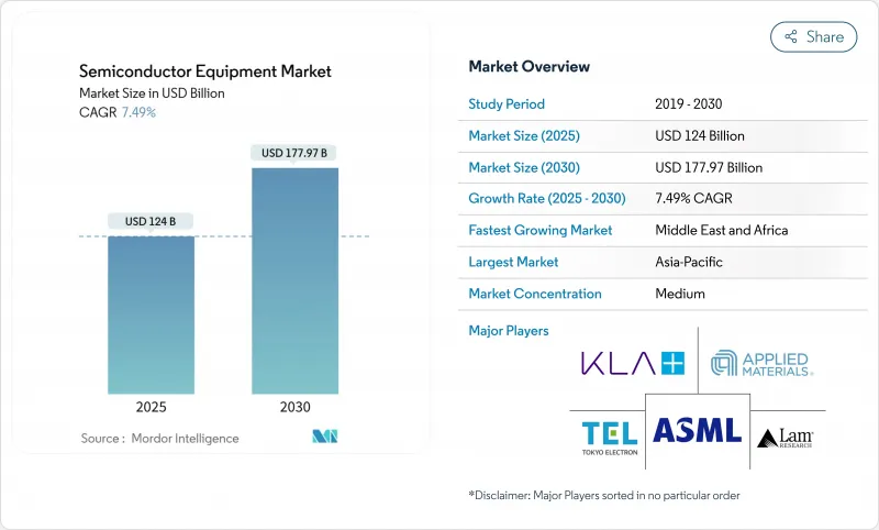
预计到 2025 年半导体设备市场规模将达到 1,240 亿美元,到 2030 年将达到 1,779.7 亿美元,复合年增长率为 7.49%。
强劲的晶圆厂建设、创纪录的设备订单以及一系列政府奖励正在支撑这一发展趋势。晶圆代工厂正加速推进2奈米以下製程的产能,而半导体组装测试外包(OSAT)公司则在扩建先进封装生产线,以满足人工智慧(AI)的需求。为实现技术主权而进行的地缘政治努力正在影响资本支出模式,迫使设备供应商在应对中国出口限制的同时,也要抓住北美、欧洲和中东的补贴机会。那些能够兼顾製程广度、软体分析和售后服务覆盖的设备製造商,正在从业内最大的投资者那里获得多年采购承诺。
全球半导体设备市场趋势与洞察
对尖端家用电器和智慧型手机的需求激增
智慧型手机、穿戴式装置和混合实境设备不断增加逻辑、储存和类比电路,这要求这些设备采用更小的製程节点进行製造,促使代工厂加速推进28nm至7nm生产线的产能提升。先进封装技术能够在不增加功耗的情况下缩小高频宽功能,在2025年初占据了相当大的营收份额,推动了凸点、测试和微影术设备的升级换代。异质整合线(垂直堆迭晶片)以两位数的成长率快速扩张,带动了覆晶键合机和晶圆级检测设备的出货量。随着消费品週期的缩短,能够快速切换配方的模组化沉积腔设备製造商正在赢得订单。在印度和东南亚,行动电话更新换代速度很快,成熟的製程节点设备几乎满载运作,证明即使在运作设备发布期间,也能实现稳定的营收成长。
对人工智慧、物联网和边缘设备节点的快速投资
资料中心营运商对高 TOPS/W 晶片的需求不断增长,推动了对 3nm 及以下製程的极紫外线 (EUV) 扫描仪和原子层沉积模组的采购。美国和欧洲的 AI 加速器新兴企业正在签订产能预订协议,将多年 HBM 采购与尖端微影术的使用保障相结合,从而将需求风险从晶片设计商转移到设备製造商。用于工厂自动化和智慧城市部署的边缘 AI 设备正在加速对 16nm 到 12nm 製程的需求,并刺激了对配备嵌入式非挥发性记忆体的 300mm 蚀刻系统的新订单。设备供应商正在将 AI 整合到原位製程监控演算法中,以缩短配方开发週期并提高腔室运作。 AI 工作负载的增加和更智慧工具的出现形成良性循环,这将使半导体设备市场在 2030 年及以后持续保持强劲成长。
极高的资本支出和漫长的投资回收期
如今,一座先进逻辑晶片工厂的成本已远超200亿美元,而尖端设备的基本客群也日益集中。漫长的折旧免税额期延长了采购尽职调查的时间,迫使设备製造商在下单前证明其多节点扩充性。供应商正透过可升级平台、模组化真空结构以及基于订阅的製程控制软体来应对这项挑战,将成本分摊到设备的整个生命週期内。一些整合装置製造商(IDM)正在推迟产能扩张、推迟设备安装,并将收入确认推迟到计划后期。然而,对每瓦性能的持续追求正在推动蓝图的製定,并限制半导体设备市场整体的下滑趋势。
细分市场分析
到2024年,晶圆前端设备将占据半导体设备市场83.7%的份额,凸显了微影术、蚀刻和沈积在产量比率方面的核心作用。在该领域,高数值孔径(NA)极紫外线(EUV)扫描器到2030年将以21.1%的复合年增长率增长,因为它们对于2nm逻辑晶片和3D DRAM结构的图形化至关重要,来自台湾和纽约晶圆厂的多系统订单已达数十亿美元。
后端製程的复杂性正在推动创新,例如具有亚2微米对准精度的热压键合机和利用前端微影术精度的扇出型晶圆级封装。将微影术光学元件、贴片机器人和高频测试模组整合到平台中的供应商正在占据越来越大的先进封装预算份额,并将微影术级投资进一步延伸至供应链下游。
到2024年,晶圆代工厂将占半导体设备市场收入的52.2%,因为无晶圆厂晶片公司将订单集中到台积电、三星晶圆代工和格罗方德等厂商。亚利桑那州、德勒斯登和高雄的大型企划配备了丛集的极紫外光刻机、多腔室蚀刻堆迭装置和原子层沉淀设备,这些设备均配置为可快速切换製程配方。严格的执行时间承诺促成了配套服务协议的签订,这些协议的价值如今已达到设备购置价值的25%至30%,从而为设备供应商创造了稳定的收入来源。
受人工智慧加速器和汽车网域控制器所需的 2.5D 和3D封装架构的推动,OSAT 厂商以 12.2% 的复合年增长率成为成长最快的客户类别。新增资本投资项目包括用于穿透硅通孔的雷射钻孔机、高密度覆晶键合机和模具底部填充剂点胶系统。整合装置製造商 (IDM) 的规模仍然可观,但由于他们采取了「轻晶圆厂」策略,即选择性地投资于电源、类比和感测器生产线,同时将尖端逻辑电路外包,因此其市场份额有所下降。
半导体设备市场按设备类型(前端设备、后端设备)、供应链参与企业(IDM、代工厂、OSAT)、晶圆尺寸(300mm、200mm、≤150mm)、晶圆製造技术节点(≥28Nm、16/14Nm、其他)、最终用户行业(计算和数据中心、北美地区和其他国家(北美地区)进行细分、其他通讯/
区域分析
亚太地区在2024年仍维持72.2%的半导体设备市场份额,主要得益于台湾、韩国和中国当地密集的产业生态系统。光是台湾的晶圆代工产业丛集的运转率就超过90%,并订单了EUV光刻和计量订单的成长。韩国加大了对1β DRAM和全环栅极逻辑装置的投入,而中国大陆则在出口限制的压力下,透过推进自主研发,提高了国内刻蚀和沈积设备的运作。
北美光刻技术的復兴得益于《晶片技术组装法案》(CHIPS Act)的津贴,奥尔巴尼奈米科技公司(Albany NanoTech)交付了全球首台高数值孔径极紫外光刻机,并为美国本土微影术生态系统奠定了基础。同时,台积电和英特尔在亚利桑那州的投资,打造了一条从奥勒冈州的设备组装到德克萨斯州的材料供应的产业走廊,重新平衡了区域需求。
欧洲计画利用《欧洲晶片法案》在2030年前将区域产能翻一番,重点发展汽车功率元件、射频前端和先进感测器等专业技术领域。萨克森州的双300毫米生产线已经整合了逻辑、类比和功率处理功能。
中东和非洲地区成长最快,复合年增长率达9.9%,主要得益于沙乌地阿拉伯90亿美元的晶圆厂建设计画和阿联酋的可行性研究。这些计划需要涵盖培训、维修和物流承包工具支援合约。南美洲市场仍处于小众阶段,巴西则选择性地投资于依赖成熟200毫米模具的汽车和工业晶片。
其他福利:
- Excel格式的市场预测(ME)表
- 3个月的分析师支持
目录
第一章 引言
- 研究假设和市场定义
- 调查范围
第二章调查方法
第三章执行摘要
第四章 市场情势
- 市场概览
- 市场驱动因素
- 对尖端家用电器和智慧型手机的需求快速成长
- 对人工智慧、物联网和边缘设备节点的快速投资
- 一系列政府补贴(CHIPS、欧盟CHIPS法案等)将推升工具资本支出。
- 向 GAA 和高数值孔径 EUV 的过渡需要新的工具集
- 永续性指示推广「绿色製造」维修工具
- 对3D异质整合封装的需求激增
- 市场限制
- 极高的资本支出和漫长的投资回收期
- 特殊材料供应瓶颈导致工具出货延迟
- 对中国工具出口的限制
- 熟练的现场服务工程师严重短缺
- 价值链分析
- 监管环境
- 技术展望
- 波特五力分析
- 供应商的议价能力
- 买方的议价能力
- 新进入者的威胁
- 替代品的威胁
- 竞争对手之间的竞争
- 宏观经济因素的影响
第五章 市场规模与成长预测
- 透过装置
- 前端装置
- 微影术设备
- 蚀刻设备
- 沉淀设备
- 测量/检测设备
- 清洁设备
- 光阻剂处理设备
- 其他前端类型
- 后端设备
- 测试设备
- 组装和包装设备
- 前端装置
- 供应链参与企业
- IDM
- 晶圆代工厂
- OSAT
- 按晶圆尺寸
- 300 mm
- 200 mm
- ≤150 毫米
- 按晶圆製造技术节点
- >=28nm
- 16/14 nm
- 10/7 nm
- 5奈米或更小
- 按最终用户行业划分
- 计算和资料中心
- 通讯(5G、射频)
- 汽车与出行
- 消费性电子产品
- 工业及其他
- 按地区
- 北美洲
- 美国
- 加拿大
- 墨西哥
- 南美洲
- 巴西
- 阿根廷
- 其他南美洲
- 欧洲
- 德国
- 英国
- 法国
- 义大利
- 西班牙
- 其他欧洲地区
- 亚太地区
- 中国
- 日本
- 韩国
- 印度
- 亚太其他地区
- 中东和非洲
- 中东
- 沙乌地阿拉伯
- 阿拉伯聯合大公国
- 土耳其
- 其他中东地区
- 非洲
- 南非
- 奈及利亚
- 埃及
- 其他非洲地区
- 北美洲
第六章 竞争情势
- 市场集中度
- 策略趋势
- 市占率分析
- 公司简介
- Applied Materials Inc.
- ASML Holding NV
- Tokyo Electron Ltd.
- Lam Research Corp.
- KLA Corp.
- Screen Holdings Co. Ltd.
- Teradyne Inc.
- Hitachi High-Tech Corp.
- Veeco Instruments Inc.
- ASM International NV
- Canon Inc.
- Nikon Corp.
- Onto Innovation Inc.
- Nova Ltd.
- Advantest Corp.
- Hanmi Semiconductor Co. Ltd.
- Disco Corp.
- BESI(BE Semiconductor Industries)
- Kulicke & Soffa Industries Inc.
- FormFactor Inc.
- Plasma-Therm LLC
- SUSS MicroTec SE
- Kokusai Electric Corp.
- AMEC(Advanced Micro-Fabrication Equipment Inc.)
- Naura Technology Group Co. Ltd.
第七章 市场机会与未来展望
The semiconductor equipment market size was valued at USD 124.00 billion in 2025 and is forecast to reach USD 177.97 billion by 2030, at a 7.49% CAGR.
Robust fab construction, record equipment backlogs, and a wave of government incentives underpin this trajectory. Foundries are accelerating capacity at 2 nm and below, while Outsourced Semiconductor Assembly and Test (OSAT) players scale advanced-package lines to serve artificial-intelligence (AI) demand. Geopolitical efforts to achieve technological sovereignty are shaping capital-spending patterns, forcing tool vendors to juggle export controls in China with subsidy-fuelled opportunities in North America, Europe, and the Middle East. Equipment makers that bundle process breadth, software analytics, and service coverage are securing multi-year purchase commitments from the sector's largest investors.
Global Semiconductor Equipment Market Trends and Insights
Surging demand for advanced consumer electronics and smartphones
Smartphones, wearables, and mixed-reality devices keep adding logic, memory, and analog content that must be built at ever-smaller nodes, pushing foundries to accelerate capacity on 28 nm-7 nm lines. Advanced packaging that miniaturizes high-bandwidth functions without raising power budgets drove a sizable share of early-2025 revenue, triggering an upgrade wave in bumping, test, and lithography equipment. Heterogeneous-integration lines stacking chiplets vertically are expanding at double-digit rates, lifting shipments of flip-chip bonders and wafer-level inspection tools. Tool makers offering modular deposition chambers with rapid recipe switching are winning orders as consumer-product cycles tighten. Strong handset refresh rates across India and Southeast Asia keep mature-node tools running near full utilization, proving that resilient billings are achievable even during premium-device launches.
Rapid AI-, IoT- and edge-device node investments
Data-center operators seek chips that offer higher TOPS-per-watt, boosting procurement of extreme ultraviolet (EUV) scanners and atomic-layer deposition modules used at 3 nm and below. AI accelerator start-ups in the United States and Europe are signing capacity reservation agreements that tie multi-year HBM purchases to guaranteed access to leading-edge lithography, shifting demand risk from chip designers to equipment makers. Edge AI devices for factory automation and smart-city deployments accelerate 16 nm-12 nm demand, spurring fresh orders for 300 mm etch systems tailored to embedded non-volatile memory. Tool suppliers deploy AI in situ process-monitoring algorithms, shortening recipe-development cycles and improving chamber uptime. The self-reinforcing loop between AI workload growth and smarter tools bolsters the semiconductor equipment market well past 2030.
Extremely high CAPEX and long pay-back cycles
A single advanced-logic fab now costs well above USD 20 billion, making the customer base for leading-edge tools increasingly concentrated. Lengthy depreciation periods stretch procurement scrutiny, compelling toolmakers to demonstrate multi-node extendibility before purchase orders are released. Vendors respond with upgrade-ready platforms, modular vacuum geometries, and subscription-based process-control software that spreads cost over a tool's life span. Some IDMs delay capacity expansions, which defers installations and shifts revenue recognition to late project phases. Nevertheless, the relentless need for performance-per-watt keeps road maps intact, limiting the overall drag on the semiconductor equipment market.
Other drivers and restraints analyzed in the detailed report include:
- Government subsidy waves are boosting the tool CAPEX
- Transition to GAA and High-NA EUV necessitates new toolsets
- Specialty-material supply bottlenecks are delaying tool shipments
For complete list of drivers and restraints, kindly check the Table Of Contents.
Segment Analysis
Front-end wafer-processing instruments captured 83.7% of the semiconductor equipment market share in 2024, underscoring the central role of lithography, etch, and deposition in yield improvement. Within this segment, High-NA EUV scanners post a 21.1% CAGR to 2030 because they are indispensable for patterning 2 nm logic and 3-D DRAM structures; multi-system orders from fabs in Taiwan and New York already total several billion USD.
Backend complexity fuels innovations such as thermo-compression bonders with sub-2 µm alignment accuracy and fan-out wafer-level packaging that leverages front-end lithographic precision. Vendors that combine lithography optics, placement robotics, and high-frequency test modules into unified platforms are capturing a growing share of advanced-package budgets, extending lithography-grade investments further down the supply chain.
Foundries accounted for 52.2% of semiconductor equipment market revenue in 2024 as fabless chip firms concentrate orders on TSMC, Samsung Foundry, and GlobalFoundries. Mega-projects in Arizona, Dresden, and Kaohsiung each feature clusters of EUV scanners, multi-chamber etch stacks, and atomic-layer deposition tools configured for rapid recipe swaps, reflecting the foundry model's need to host diverse customer process flows. Strict uptime commitments drive bundled service contracts that now equal 25-30% of tool acquisition value, creating annuity streams for equipment suppliers.
OSAT houses emerge as the fastest-growing customer category at a 12.2% CAGR, propelled by 2.5-D and 3-D package architectures required for AI accelerators and automotive domain controllers. New capex lines include laser-drilling for through-silicon vias, high-density flip-chip bonders, and molded-underfill dispense systems. Integrated device manufacturers (IDMs) retain a sizeable but declining share as they pursue fab-lite strategies that outsource leading-edge logic while investing selectively in power, analog, and sensor lines.
Semiconductor Equipment Market is Segmented by Equipment Type (Front-End Equipment, and Back-End Equipment), Supply Chain Participant (IDM, Foundry, and OSAT), Wafer Size (300 Mm, 200 Mm, and <=150 Mm), Fab Technology Node (>=28 Nm, 16/14 Nm, and More), End-User Industry (Computing and Data-Center, Communications (5G, RF), and More), and Geography (North America, South America, Europe, Asia-Pacific, and Middle East and Africa).
Geography Analysis
Asia-Pacific retained 72.2% semiconductor equipment market share in 2024, powered by dense ecosystems in Taiwan, South Korea, and mainland China; Taiwan's foundry cluster alone ran above 90% utilization, sustaining EUV and metrology orders. South Korea intensified spending on 1-beta DRAM and gate-all-around logic, while China's drive for self-reliance lifted domestic etcher and deposition installations even under export-control pressure.
North America's renaissance stems from CHIPS Act grants; Albany NanoTech took delivery of the world's first High-NA EUV tool, creating a cornerstone for a domestic lithography ecosystem. Simultaneous investments by TSMC and Intel in Arizona form a corridor stretching from equipment assembly in Oregon to materials supply in Texas, re-balancing regional demand.
Europe sharpened its specialty-technology focus-automotive power devices, RF front-ends, and advanced sensors-using the European Chips Act to target a doubling of regional capacity by 2030; Saxony's dual 300 mm lines already combine logic, analog, and power processing.
The Middle East and Africa logged the fastest growth at 9.9% CAGR, fuelled by Saudi Arabia's USD 9 billion fab plan and UAE feasibility studies, which require turnkey tool-support contracts spanning training, refurbishment, and logistics. South America remains niche; Brazil is investing selectively in automotive and industrial chips that rely on mature-node 200 mm tools.
- Applied Materials Inc.
- ASML Holding NV
- Tokyo Electron Ltd.
- Lam Research Corp.
- KLA Corp.
- Screen Holdings Co. Ltd.
- Teradyne Inc.
- Hitachi High-Tech Corp.
- Veeco Instruments Inc.
- ASM International NV
- Canon Inc.
- Nikon Corp.
- Onto Innovation Inc.
- Nova Ltd.
- Advantest Corp.
- Hanmi Semiconductor Co. Ltd.
- Disco Corp.
- BESI (BE Semiconductor Industries)
- Kulicke & Soffa Industries Inc.
- FormFactor Inc.
- Plasma-Therm LLC
- SUSS MicroTec SE
- Kokusai Electric Corp.
- AMEC (Advanced Micro-Fabrication Equipment Inc.)
- Naura Technology Group Co. Ltd.
Additional Benefits:
- The market estimate (ME) sheet in Excel format
- 3 months of analyst support
TABLE OF CONTENTS
1 INTRODUCTION
- 1.1 Study Assumptions and Market Definition
- 1.2 Scope of the Study
2 RESEARCH METHODOLOGY
3 EXECUTIVE SUMMARY
4 MARKET LANDSCAPE
- 4.1 Market Overview
- 4.2 Market Drivers
- 4.2.1 Surging demand for advanced consumer electronics and smartphones
- 4.2.2 Rapid AI-, IoT- and edge-device node investments
- 4.2.3 Government subsidy waves (CHIPS, EU Chips Act, etc.) boosting tool CAPEX
- 4.2.4 Transition to GAA and High-NA EUV necessitating new toolsets
- 4.2.5 Sustainability mandates driving "green fab" retrofit tools
- 4.2.6 3D heterogeneous-integration packaging demand spike
- 4.3 Market Restraints
- 4.3.1 Extremely high CAPEX and long pay-back cycles
- 4.3.2 Specialty-material supply bottlenecks delaying tool shipments
- 4.3.3 Export-control restrictions on China-bound tools
- 4.3.4 Acute shortage of skilled field-service engineers
- 4.4 Value Chain Analysis
- 4.5 Regulatory Landscape
- 4.6 Technological Outlook
- 4.7 Porter's Five Forces Analysis
- 4.7.1 Bargaining Power of Suppliers
- 4.7.2 Bargaining Power of Buyers
- 4.7.3 Threat of New Entrants
- 4.7.4 Threat of Substitutes
- 4.7.5 Intensity of Competitive Rivalry
- 4.8 Impact of Macroeconomic Factors
5 MARKET SIZE AND GROWTH FORECASTS (VALUE)
- 5.1 By Equipment Type
- 5.1.1 Front-end Equipment
- 5.1.1.1 Lithography Equipment
- 5.1.1.2 Etch Equipment
- 5.1.1.3 Deposition Equipment
- 5.1.1.4 Metrology / Inspection Equipment
- 5.1.1.5 Cleaning Equipment
- 5.1.1.6 Photoresist Processing Equipment
- 5.1.1.7 Other Front-end Types
- 5.1.2 Back-end Equipment
- 5.1.2.1 Test Equipment
- 5.1.2.2 Assembly and Packaging Equipment
- 5.1.1 Front-end Equipment
- 5.2 By Supply-Chain Participant
- 5.2.1 IDM
- 5.2.2 Foundry
- 5.2.3 OSAT
- 5.3 By Wafer Size
- 5.3.1 300 mm
- 5.3.2 200 mm
- 5.3.3 <=150 mm
- 5.4 By Fab Technology Node
- 5.4.1 >=28 nm
- 5.4.2 16/14 nm
- 5.4.3 10/7 nm
- 5.4.4 5 nm and below
- 5.5 By End-user Industry
- 5.5.1 Computing and Data-Center
- 5.5.2 Communications (5G, RF)
- 5.5.3 Automotive and Mobility
- 5.5.4 Consumer Electronics
- 5.5.5 Industrial and Others
- 5.6 By Geography
- 5.6.1 North America
- 5.6.1.1 United States
- 5.6.1.2 Canada
- 5.6.1.3 Mexico
- 5.6.2 South America
- 5.6.2.1 Brazil
- 5.6.2.2 Argentina
- 5.6.2.3 Rest of South America
- 5.6.3 Europe
- 5.6.3.1 Germany
- 5.6.3.2 United Kingdom
- 5.6.3.3 France
- 5.6.3.4 Italy
- 5.6.3.5 Spain
- 5.6.3.6 Rest of Europe
- 5.6.4 Asia-Pacific
- 5.6.4.1 China
- 5.6.4.2 Japan
- 5.6.4.3 South Korea
- 5.6.4.4 India
- 5.6.4.5 Rest of Asia-Pacific
- 5.6.5 Middle East and Africa
- 5.6.5.1 Middle East
- 5.6.5.1.1 Saudi Arabia
- 5.6.5.1.2 United Arab Emirates
- 5.6.5.1.3 Turkey
- 5.6.5.1.4 Rest of Middle East
- 5.6.5.2 Africa
- 5.6.5.2.1 South Africa
- 5.6.5.2.2 Nigeria
- 5.6.5.2.3 Egypt
- 5.6.5.2.4 Rest of Africa
- 5.6.1 North America
6 COMPETITIVE LANDSCAPE
- 6.1 Market Concentration
- 6.2 Strategic Moves
- 6.3 Market Share Analysis
- 6.4 Company Profiles (includes Global-level Overview, Market-level Overview, Core Segments, Financials as available, Strategic Information, Market Rank/Share, Products and Services, Recent Developments)
- 6.4.1 Applied Materials Inc.
- 6.4.2 ASML Holding NV
- 6.4.3 Tokyo Electron Ltd.
- 6.4.4 Lam Research Corp.
- 6.4.5 KLA Corp.
- 6.4.6 Screen Holdings Co. Ltd.
- 6.4.7 Teradyne Inc.
- 6.4.8 Hitachi High-Tech Corp.
- 6.4.9 Veeco Instruments Inc.
- 6.4.10 ASM International NV
- 6.4.11 Canon Inc.
- 6.4.12 Nikon Corp.
- 6.4.13 Onto Innovation Inc.
- 6.4.14 Nova Ltd.
- 6.4.15 Advantest Corp.
- 6.4.16 Hanmi Semiconductor Co. Ltd.
- 6.4.17 Disco Corp.
- 6.4.18 BESI (BE Semiconductor Industries)
- 6.4.19 Kulicke & Soffa Industries Inc.
- 6.4.20 FormFactor Inc.
- 6.4.21 Plasma-Therm LLC
- 6.4.22 SUSS MicroTec SE
- 6.4.23 Kokusai Electric Corp.
- 6.4.24 AMEC (Advanced Micro-Fabrication Equipment Inc.)
- 6.4.25 Naura Technology Group Co. Ltd.
7 MARKET OPPORTUNITIES AND FUTURE OUTLOOK
- 7.1 White-space and Unmet-Need Assessment
 半导体製造设备市场分析及预测(至2035年):依类型、产品、技术、组件、应用、材料类型、装置、製程、最终用户及製造阶段划分
 扫描电子显微镜维修服务市场:按服务类型、应用和最终用户划分,全球预测(2026-2032年)显微镜目镜筒市场:按类型、材料、分销管道、应用和最终用户划分,全球预测,2026-2032年等离子切割系统市场:按设备类型、晶圆尺寸、晶圆厚度、最终用户和应用划分,全球预测,2026-2032年生物洁净作业台市场按产品类型、应用和最终用户划分,全球预测(2026-2032年)冷冻肉切丁机市场按机器类型、自动化程度、产能、终端用户产业、应用和销售管道划分,全球预测(2026-2032年)人工智慧市场分析及产量比率(至2035年):按类型、产品类型、服务、技术、组件、应用、部署类型、最终用户和设备划分人工智慧市场分析及预测(至2035年),展望半导体发展趋势:依类型、产品、服务、技术、组件、应用、製程、部署、最终用户及功能划分以半导体产量比率预测为导向的人工智慧市场分析及预测(至2035年):按类型、产品、服务、技术、组件、应用、製程、部署、最终用户和解决方案划分半导体产业的AI节水市场分析及预测(至2035年):依类型、产品类型、服务、技术、组件、应用、製程、最终用户及解决方案划分