


 |
市场调查报告书
商品编码
1438411
面板级封装:市场占有率分析、产业趋势与统计、成长预测(2024-2029)Panel Level Packaging - Market Share Analysis, Industry Trends & Statistics, Growth Forecasts (2024 - 2029) |
||||||
※ 本网页内容可能与最新版本有所差异。详细情况请与我们联繫。
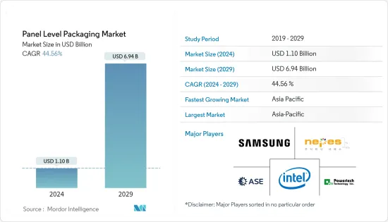
预计2024年面板级封装市场规模为11亿美元,预计2029年将达到69.4亿美元,在预测期间(2024-2029年)复合年增长率为44.56%。
半导体产业正在经历快速成长,半导体已成为所有现代技术的基本组成部分。该领域的进步和创新对所有下游技术产生直接影响,从而推动了市场研究的需求。
主要亮点
- 400mm 晶圆需求正在转向面板级封装。面板级封装是晶圆层次电子构装扇出之后的一步。世界各地的供应商都专注于扩展 PLP,而不是製定 450mm晶圆层次电子构装的蓝图。此外,PLP 预计将透过并行化製程步骤并在矩形面板格式封装(而不是圆形晶圆几何形状)中实现更高的面积利用率来提供显着的成本效益,从而减少材料浪费。
- 然而,随着封装尺寸从晶圆到更大的面板格式的增加,此外,并行製造的封装数量的增加,成本优势导致向面板级封装的转变正受到越来越多的关注。此外,PLP 可以采用其他技术领域的製程、材料和设备。印刷基板(PCB)、液晶显示器 (LCD) 和太阳能电池均以面板尺寸製造,提供了新的扇出面板级封装方法。
- 此外,消费性电子和汽车等各种最终用户行业的小型化趋势也给封装供应商带来了越来越大的压力。从覆晶到晶圆层次电子构装的转变是一个已经持续多年的趋势。然而,下一类先进封装正在从 300mm 晶圆级封装转向面板级封装。
- 封装製程有两种类型:先模具和先 RDL。然而,晶片移位是这种类型封装的一个问题。晶片移位被认为是最大的问题之一,因为它会降低产量比率或对产量比率产生负面影响。这增加了对包装过程进行更好控制的需求并增加了复杂性。
- COVID-19大流行从需求和供应双方影响了整个半导体製造市场。此外,全球半导体工厂停工或关闭加剧了供不应求。这种影响也体现在面板级封装市场。然而,其中许多影响将是短期的。世界各国政府为支持汽车和半导体产业所采取的预防措施可能会重振产业成长。
面板级封装市场趋势
对小型、高性能电子设备的需求不断增长,预计将占据很大份额
- 消费性电子产品是市场上主要的最终用户产业之一。智慧型手机产业的成长、智慧型装置和穿戴式装置的日益普及,以及消费者物联网装置在智慧家庭等应用中的普及不断提高,是推动所研究细分市场成长的关键因素。
- 消费性电子产业的小型化趋势正在创造更小、更轻、更可携式的设备。消费性电子产品中的每一款新产品都比其前身更具创新性、更轻且更节能。这让客户对下一次迭代产生了很高的期望,使其成为家电生产商的关键卖点。先进的半导体封装技术有助于满足消费性电子市场复杂且不断变化的需求。
- 由于对高性能、高能效、薄型和小尺寸封装的需求,面板级封装越来越多地用于智慧型手机等空间敏感型设备。因此,近年来这些设备的日益普及也为该市场创造了巨大的需求。例如,根据爱立信的数据, 年终智慧型手机相关合约数量为63亿份,约占行动电话合约总数的77%。这项预测预计到 2027 年订阅量将达到 78 亿,约占所有行动电话订阅量的 87%。
- 扇出面板级封装 (FOPLP) 因其许多优点(包括低成本潜力)而在许多家用电子电器应用中稳步普及。目前,采用此技术的主流整合晶片包括用于5G智慧型手机的封装天线(AiP)天线模组、用于穿戴式装置的整合晶片以及物联网(IoT)用例。
- 这样,近期5G和物联网的普及为市场带来了显着的成长机会。例如,根据GSMA的预测,2025年,5G网路预计将覆盖全球三分之一的人口。该组织也预测,到年终年底,5G连线数将超过10亿,到2025年将超过20亿,占行动连线的五分之一以上。
- 随着5G投资的增加,对相容5G的智慧型手机的需求也随之增加。例如,根据消费者技术协会(CTA)的数据,2022年5G智慧型手机的收益预计将达到613.7亿美元,比2021年的533.8亿美元成长15%。预计2021年5G智慧型手机将占所有智慧型手机销量的62%,2022年将上升至72%。
亚太地区预计将占据较大份额
- 台湾因其强大的ICT产业基础、坚实的半导体製造群和先进的製造能力而被誉为电子製造中心。这些优势促进了许多提供先进ICT相关产品的本地公司的快速发展,主要集中在电子元件、电脑、光纤电缆和通讯设备领域。
- 该地区也受益于台积电和日月光等大型半导体公司的存在,这些公司专注于投资先进的半导体封装解决方案。台积电已在台湾北部运作四家先进封装工厂,分别位于新竹科学园区(HSP)、中央科学园区(CTSP)、南部科学园区(STSP)和龙塘。该公司目前计划在台湾南部的嘉义市或云林县建立一座新的先进封装工厂。
- 台湾最近宣布额外支出 2,369.6 亿新台币(85.6 亿美元),用于在未来五年内采购武器,以应对中国的威胁。这笔独特的预算预计将主要用于2022年至2026年购买本土武器系统。此类投资预计将进一步促进半导体元件的使用,从而对市场产生积极影响。
- 此外,日本的通讯市场也是全球收入最大的电信市场之一,儘管整体市场受到经济和人口增长缓慢的支撑,但在过去二十年中,日本在铁塔和光纤基础设施方面投入了大量资金。固定/行动网路营运商。
- 汽车产业占该国半导体零件总需求的很大一部分。此外,增加自动驾驶汽车采用的措施也进一步推动了市场成长。
面板级封装产业概述
该市场主要由三星电子、英特尔公司、Nepes公司、日月光集团和PowerTech科技公司主导,这些公司在市场上占有很大份额。然而,在未来几年,我们预计将有更多的公司参与广泛的研发和市场开拓活动,以开发有竞争力的面板级封装技术。
- 2022 年 7 月 - Nepes 宣布将增加使用最先进的封装技术之一——扇出面板级封装 (FO-PLP) 进行量产的产品数量。电源管理积体电路(PMIC)之后将是转码器晶片和应用处理器。
- 2022 年 2 月-英特尔以每股 530 亿美元现金收购 Tower Semiconductor。此次收购是英特尔IDM 2.0策略的重大进步,因为该公司进一步扩大了製造能力,扩大了封装技术、全球足迹和技术组合,以满足业界前所未有的需求。
其他福利:
- Excel 格式的市场预测 (ME) 表
- 3 个月分析师支持
目录
第一章 简介
- 研究假设和市场定义
- 调查范围
第二章调查方法
第三章执行摘要
第四章市场洞察
- 市场概况
- 产业吸引力-波特五力分析
- 供应商的议价能力
- 买方议价能力
- 新进入者的威胁
- 替代品的威胁
- 竞争公司之间的敌对关係
- 产业价值链分析
- COVID-19 市场影响评估
第五章市场动态
- 市场驱动因素
- 降低包装过程成本
- 对小型和高性能电子设备的需求不断增长
- 加大研发投入
- 市场限制因素
- 包装工艺复杂
第六章市场区隔
- 按工业用途
- 消费性电子产品
- 车
- 通讯
- 其他工业应用
- 按地区
- 美国
- 中国
- 韩国
- 台湾
- 日本
- 欧洲
- 世界其他地区
第七章 竞争形势
- 公司简介
- Samsung Electronics Co. Ltd
- Intel Corporation
- Nepes Corporation
- ASE Group
- Powertech Technology Inc.
- Fraunhofer Institute for Reliability and Micro integration IZM
- Unimicron Technology Corporation
- DECA Technologies Inc.
- JCET/STATSChipPAC
第八章投资分析
第9章市场的未来
The Panel Level Packaging Market size is estimated at USD 1.10 billion in 2024, and is expected to reach USD 6.94 billion by 2029, growing at a CAGR of 44.56% during the forecast period (2024-2029).
The semiconductor industry is witnessing rapid growth, with semiconductors emerging as the basic building blocks of all modern technology. The advancements and innovations in this field directly impact all downstream technologies and drive the market study's need.
Key Highlights
- The need for 400 mm wafers is shifting focus toward panel-level packaging. Panel-level packaging is one of the following steps for Fan-out wafer-level packaging. Vendors across the globe are focusing on upscaling PLP instead of drawing a roadmap to 450 mm Fan-out Wafer Level Packaging. In addition, PLP is expected to offer significant cost advantages by parallelizing process steps and allowing higher area utilization of packages in rectangular panel formats rather than round wafer shapes to lower material waste.
- However, the focus on Panel Level Packaging is increasing due to the cost benefits and expanding the packaging size from wafer to larger panel formats and, in addition to that, increasing the number of packages manufactured in parallel. Additionally, PLP can adopt processes, materials, and equipment from other technology areas. Printed Circuit Board (PCB), Liquid Crystal Display (LCD), or solar equipment is manufactured on panel sizes and offers new Fan-out Panel Level Packaging approaches.
- Moreover, the constant trend of miniaturization across various end-user industries, such as consumer electronics, automotive, and others, has also increased pressure on packaging vendors. The transition from Flip-Chip to Wafer Level packaging has continued to be a trend for several years. However, the following type of advanced packaging is shifting from 300mm wafer-level packaging to Panel level packaging.
- The packaging process involves both types, Mold first and RDL first. However, the type of packaging involves problems in die shift. Die shifting is considered one of the biggest issues as it may cause lesser yield or negatively influence the yields. This increases the need for more control over the packaging process and adds complexity.
- The COVID -19 pandemic affected the overall semiconductor manufacturing market from the demand and supply sides. In addition, the global lockdowns and closure of semiconductor plants further fueled the supply shortage. The effects were also reflected in the Panel level packaging market. However, many of these effects are likely to be short-term. Precautions by governments across the globe to support automotive and semiconductor sectors could help revive industry growth.
Panel Level Packaging Market Trends
Increasing demand for compact, high functionality electronic devices is Expected to Hold Major Share
- Consumer electronics is one of the major end-user industries in the market. Growth in the smartphone industry, increasing adoption of smart devices and wearables, and increasing penetration of consumer IoT devices in applications like smart homes are significant factors driving the growth of the studied segment.
- The miniaturization trend in the consumer electronics industry has given rise to smaller, lighter, and more portable devices. Each new iteration of consumer electronics products is more innovative, lightweight, and energy-efficient than its predecessors. This creates enormous customer expectations for the next iteration, which is a significant selling point for the producers of consumer electronics. Advanced semiconductor packaging technologies can help meet the consumer electronics market's complex and evolving needs.
- Panel-level packaging has been finding increasing applications in footprint-sensitive devices, such as smartphones, owing to the requirement of high-performing, energy-efficient, thin, and small form factor packages. As such, the growing penetration of these devices in recent years also create considerable demand for the market. For instance, as per Ericsson, there were 6.3 billion subscriptions associated with smartphones at the end of 2021, accounting for about 77% of all mobile phone subscriptions. This forecast is expected to reach 7.8 billion in 2027, accounting for around 87% of all mobile subscriptions.
- The popularity of fan-out panel level packaging (FOPLP) has been rising steadily for many consumer electronic applications due to its many advantages, including low-cost potential. The current mainstream chips that use this technology for integration include Antenna-in-Package (AiP) antenna modules of 5G smartphones, integrated chips of wearable devices, and Internet of Things (IoT) use cases.
- As such, the increasing penetration of 5G and IoT in recent years presents significant growth opportunities for the market. For instance, as per GSMA, by 2025, 5G networks are expected to cover one-third of the world's population. The organization has also predicted that the number of 5G connections will surpass 1 billion by the end of 2022 and 2 billion by 2025, making up over a fifth of mobile connections.
- With the rising investments in 5G, the demand for 5G-enabled smartphones is also increasing parallelly. For instance, as per the Consumer Technology Association (CTA), the revenues from 5G smartphones are expected to reach USD 61.37 billion in 2022, up 15% from USD 53.38 billion in 2021. 5G smartphones were also estimated to make up 62% of all smartphone units in 2021 and rise to 72% in 2022.
Asia pacific is Expected to Hold Significant Share
- Taiwan is a well-known electronics manufacturing hub owing to its strong ICT industry base, robust semiconductor manufacturing clusters, and advanced manufacturing capacity. These advantages have contributed to the rapid development of many regional companies that offer advanced ICT-related products, primarily in the sectors of electronic components, computers, fiber optic cable, telecommunications equipment, etc.
- The region also benefits from the presence of large semiconductor companies like TSMC and ASE that are focusing on investing in advanced semiconductor packaging solutions. TSMC already operates four advanced packaging fabs, located in Hsinchu Science Park (HSP), Central Taiwan Science Park (CTSP), Southern Taiwan Science Park (STSP), and Longton in northern Taiwan. The company now aims to build a new advanced packaging plant in Chiayi or Yunlin county, southern Taiwan.
- Taiwan has recently declared an extra spending bill of TWD 236.96 billion (USD 8.56 billion) to procure weaponry over the next five years to counter the threats posed by China. This unique budget is expected to be used primarily to purchase indigenous weapon systems from 2022 to 2026. Such investments are expected to drive the usage of semiconductor components further, thereby positively impacting the market.
- Moreover, the Japanese telecommunications market is also one of the largest in the world by revenue, with few large fixed and mobile network operators that have invested heavily in towers and fiber infrastructure over the past two decades despite an overall market underpinned by low economic and population growth.
- The automotive industry accounts for a significant share of the country's total demand for semiconductor components. Also, the steps taken to increase the adoption of autonomous vehicles further drive the growth of the market.
Panel Level Packaging Industry Overview
The market is considered moderately competitive with major players such as Samsung Electronics, Intel Corporation, Nepes Corporation, ASE Group, and PowerTech Technology Inc. These companies have a major share of the market. However, more companies will be involved in extensive R&D and market development activities to develop competitive panel-level packaging technology in the coming years.
- July 2022 - Nepes announced that it would increase the number of products it produces in huge quantities utilizing fan-out-panel level packages (FO-PLP), one of the most advanced packaging techniques. Following the Power Management Integrated Circuit (PMIC), codec chips and application processors will be introduced to the market.
- February 2022 - Intel acquired Tower semiconductors for USD 53 billion per share in cash. The acquisition significantly advances Intel's IDM 2.0 strategy as the company further expands its manufacturing capacity, expand packaging technologies, global footprint, and technology portfolio to address unprecedented industry demand.
Additional Benefits:
- The market estimate (ME) sheet in Excel format
- 3 months of analyst support
TABLE OF CONTENTS
1 INTRODUCTION
- 1.1 Study Assumptions and Market Definition
- 1.2 Scope of the Study
2 RESEARCH METHODOLOGY
3 EXECUTIVE SUMMARY
4 MARKET INSIGHTS
- 4.1 Market Overview
- 4.2 Industry Attractiveness - Porter's Five Forces Analysis
- 4.2.1 Bargaining Power of Suppliers
- 4.2.2 Bargaining Power of Buyers
- 4.2.3 Threat of New Entrants
- 4.2.4 Threat of Substitutes Products
- 4.2.5 Intensity of Competitive Rivalry
- 4.3 Industry Value Chain Analysis
- 4.4 Assessment of the Impact of COVID-19 on the Market
5 MARKET DYNAMICS
- 5.1 Market Drivers
- 5.1.1 Reduced Cost of Packaging Process
- 5.1.2 Increasing Demand for Compact, High Functionality Electronic Devices
- 5.1.3 Increased Investment on Research & Development Activities
- 5.2 Market Restraints
- 5.2.1 Complexity in Packaging Process
6 MARKET SEGMENTATION
- 6.1 By Industry Application
- 6.1.1 Consumer Electronics
- 6.1.2 Automotive
- 6.1.3 Telecommunication
- 6.1.4 Other Industry Application
- 6.2 By Geography
- 6.2.1 United States
- 6.2.2 China
- 6.2.3 Korea
- 6.2.4 Taiwan
- 6.2.5 Japan
- 6.2.6 Europe
- 6.2.7 Rest of the World
7 COMPETITIVE LANDSCAPE
- 7.1 Company Profiles*
- 7.1.1 Samsung Electronics Co. Ltd
- 7.1.2 Intel Corporation
- 7.1.3 Nepes Corporation
- 7.1.4 ASE Group
- 7.1.5 Powertech Technology Inc.
- 7.1.6 Fraunhofer Institute for Reliability and Micro integration IZM
- 7.1.7 Unimicron Technology Corporation
- 7.1.8 DECA Technologies Inc.
- 7.1.9 JCET/ STATSChipPAC
8 INVESTMENT ANALYSIS
9 FUTURE OF THE MARKET
 2024-2028年全球高阶半导体封装市场
 2024-2032 年半导体封装市场报告(按类型、封装材料、技术、最终用户和地区)
 3D TSV:重要课题的考察与市场的分析
 高密度实装(MCM,MCP,SIP,3D-TSV):市场分析及技术趋势
 2.5D 和 3D 半导体封装 - 市场占有率分析、产业趋势与统计、成长预测(2024 - 2029)
 全球半导体封装市场规模、份额、成长分析(按材料、按应用)- 2023-2030 年产业预测
 2024 年 3D 半导体封装全球市场报告
 先进半导体封装市场报告:2030 年趋势、预测与竞争分析
 嵌入式晶片封装市场报告:2030 年趋势、预测与竞争分析
 面板级封装报告:2030 年趋势、预测与竞争分析